PCB Design Services Tailored to Your Product Needs

IWDF Solutions designs PCBs that balance performance, reliability, and manufacturability. From simple prototypes to complex boards, we help electronics companies bring products to market faster — with fewer redesigns and smoother& faster handoff to production.


IWDF PCB Design Services

Professional PCB Design Services Tailored to Your Product Needs

IWDF Solutions designs PCBs that balance performance, reliability, and manufacturability. From simple prototypes to complex boards, we help electronics companies bring products to market faster — with fewer redesigns and smoother& faster handoff to production.

Why Choose IWDF Solutions for PCB Design

We connect design innovation with production reality, ensuring every PCB is engineered for performance, reliability, and smooth transition to manufacturing.

Design Meets Manufacturing

Design Meets Manufacturing

We integrate DFM and DFT principles from the start, so every design is optimized for smooth prototyping and scalable production — reducing costly redesigns later.

Faster Validation

Faster Validation

Our engineers run SI, PI, and thermal simulations before prototyping. This shortens testing cycles and helps you move from concept to market with confidence.

Smarter Cost Decisions

Smarter Cost Decisions

By selecting the right materials and stack-ups, we balance performance with budget. You get a reliable board design without unnecessary cost or over-engineering.

Seamless Handoff

Seamless Handoff

We don’t just deliver schematics. You receive a full design package — Gerber, BOM, and assembly files — ready for any global manufacturer to build and test.

Our PCB Design Capabilities
We Design Every PCB with Production in Mind

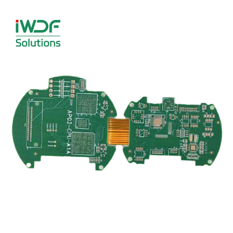
From single-layer pcb to complex multilayer, rigid-flex, heavy copper, HDI, and high-speed boards — IWDF Solutions delivers complete PCB design services. Our engineers can start from your concept or refine your existing design, create fully functional prototypes, integrate embedded software, run thorough performance testing, and provide complete production-ready documentation.

What We Offer:

Service Area

Description

Advanced Design Specialties

Complex applications—like 5G modules, power electronics, or wearable devices—demand more than just basic layout skills. We specialize in high-speed, high-frequency, heavy copper, and multilayer PCB design, ensuring your boards meet performance, reliability, and manufacturability goals from the start.

High-Speed Design

Ensures signal integrity in DDR, USB 3.0, PCIe, and high-speed buses.
Controlled impedance ±10%, length matching, signal simulation.

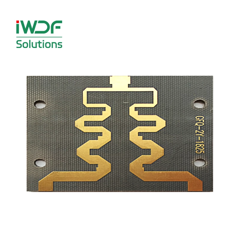
High-Frequency

Prevents signal loss in RF circuits for IoT, antennas, wireless modules.
Up to 6 GHz support, RF path tuning, antenna matching, low-loss stackup.

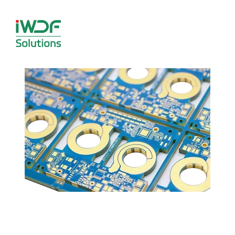
Heavy Copper PCB

Handles high current and thermal dissipation in power electronics.
Up to 6 oz copper, IPC-2221-based design, via stitching for current paths.

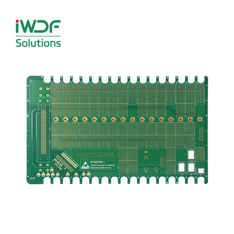
Multilayer & HDI PCB

Enables compact form factors for advanced electronics (wearables, medical, etc.)
32 layers, blind/buried vias, BGA escape routing, impedance modeling

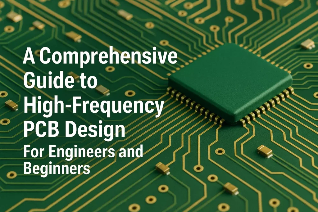
High-Speed & High-Frequency PCB Design

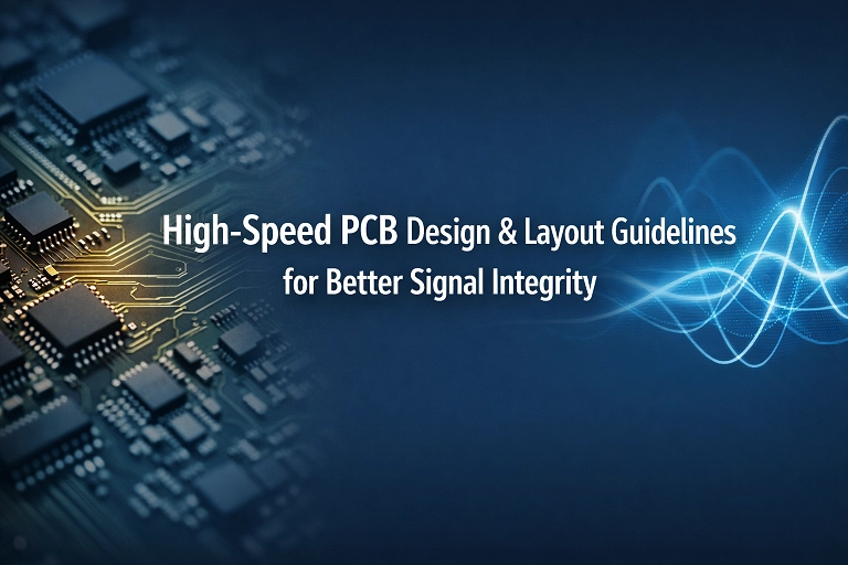
From DDR memory to USB 3.1, high-speed digital systems require precise impedance control, minimal skew, and optimal trace topology. Our team applies real-world signal integrity techniques to avoid reflections, crosstalk, and timing issues.

  • Impedance-controlled routing (±10% tolerance)
  • Length matching for differential pairs
  • Support for DDR3/DDR4, PCIe, USB, HDMI
  • Simulation-driven layout with validation tools

Multilayer & HDI PCB Design

Compact products—from medical devices to smart wearables—require high-density interconnects, stacked vias, and tightly packed layouts. We help you reduce board size while improving signal isolation and reliability.

  • Up to 32-layer stackups with blind/buried vias
  • BGA fan-out and via-in-pad routing
  • High routing density with EMI optimization
  • Balanced layer planning for thermal and mechanical performance

Heavy Copper PCB Design

Power electronics and motor controllers require PCBs that can handle high current and thermal loads. We support heavy copper designs up to 6 oz with optimized trace width and thermal management.

  • Copper thickness: 1–6 oz
  • IPC-2221 compliant trace width & via planning
  • Thermal relief, heat dissipation path design
  • Designed for EVs, industrial drives, and LED drivers

PCB Design Process丨From Idea to Production-Ready Files in 6 Steps

Requirements Analysis

1. Requirements Analysis & Design Specificatione

We begin by deeply understanding your project goals, target application, performance requirements, mechanical constraints, and budget.

  • Interface with your engineering or product team
  • Define board size, layer count, materials, impedance targets
  • Identify key functional blocks and design priorities
  • Recommend solutions based on cost, performance, and manufacturability
Schematic Capture

2. Schematic Capture & Component Selection

Once the concept is clear, we translate functional requirements into an optimized schematic design using professional EDA tools (Altium, OrCAD, KiCad, etc.).

  • Create clean, hierarchical schematics
  • Select components with lifecycle, cost, and lead-time in mind
  • Ensure library symbols and footprints are accurate and up-to-date
  • Consider alternatives for critical or long-lead parts
PCB Layout

3. PCB Layout & High-Speed Routing

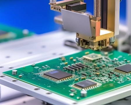
This is where the real engineering finesse comes in — transforming schematics into manufacturable layouts.

  • Placement optimized for signal integrity, thermal management, and EMI/EMC
  • High-speed routing for DDR, PCIe, HDMI, USB 3.0, etc.
  • Controlled impedance routing, matched-length traces
  • Integration of Design for Manufacturing (DFM) and Design for Testability (DFT)
  • Layer stackup planning for HDI and multilayer boards (up to 32 layers)

4. Design Review & DFM/DFA Validation

Every design goes through internal cross-checks and DFM/DFA/DFT analysis to ensure it’s ready for fabrication and assembly without surprises.

  • Design rule checks (DRC)
  • Assembly and stencil layer reviews
  • Silkscreen optimization
  • Gerber, ODB++, and drill file generation

Optional: We run the design past your contract manufacturer for joint validation.

Making a PCB Sample

5. Gerber File Generation & Manufacturing Handoff

Once the layout is finalized, we prepare a complete manufacturing documentation package:

  • Gerber, Excellon drill files, BOM, pick-and-place files
  • Assembly drawings and fabrication notes
  • Stackup diagrams, impedance control requirements
  • Netlist and component coordinate outputs
  • 3D step file for enclosure/assembly integration
esting and Making It Better

6. Support for Assembly & Testing

After design handoff, we stay involved to ensure smooth production and validation:

  • Assist in prototype assembly and debugging
  • Provide firmware or test script interface (if required)
  • Coordinate with your contract manufacturer (CM)
  • Perform design updates based on testing feedback
  • Help with regulatory compliance (EMC, CE, FCC)

Industries We Serve

Trusted PCB Design Partner Across Diverse Industries

Our PCB design solutions support a wide range of applications — from high-volume consumer devices to mission-critical aerospace systems.
We understand each industry’s technical standards, cost structure, and certification challenges.

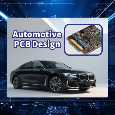
Automotive systems demand safety, temperature stability, and long-term reliability.
We design and optimize PCBs for Tier 1 and Tier 2 automotive suppliers, ensuring compliance with AEC-Q100/200 and IATF 16949 requirements.

Typical Applications:
Engine control units (ECUs), transmission control modules, BMS (Battery Management Systems), on-board chargers, ADAS radar modules, ultrasonic sensors, camera modules, infotainment systems, car lighting controllers, dashboard displays, door lock controllers, seat heating systems, smart mirrors, air conditioning control boards, vehicle networking units, EV chargers, and parking assist systems.

How We Help:

  • High-temperature and vibration-resistant layout

  • Power and signal isolation design

  • EMC/EMI optimization and differential pair routing

  • DFM and PPAP documentation for automotive compliance

Reliability beyond altitude — for systems that cannot fail.
We deliver PCBs designed for extreme environments, vibration, radiation, and mission-critical performance.

Typical Applications:
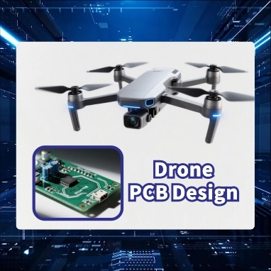
Flight control systems, avionics modules, satellite communication units, radar systems, GPS receivers, telemetry and tracking boards, data acquisition systems, navigation control boards, missile guidance electronics, and aircraft power modules.

How We Help:

  • Lightweight, high-Tg, and polyimide-based materials

  • Radiation- and vibration-resistant layout

  • Metal-core PCB and thermal management design

  • Full documentation under IPC Class 3 & MIL-STD standards

Fast-paced innovation requires compact, high-density, and cost-efficient PCB design.
Our engineering team supports consumer electronics companies in shortening product cycles and improving reliability across mass production.
Typical Applications:
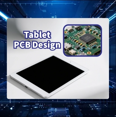
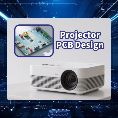
Smartphones, tablets, e-book readers, smart watches, wireless earbuds, gaming consoles, VR/AR headsets, Bluetooth speakers, MP3/MP4 players, digital cameras, set-top boxes, televisions, projectors, electronic photo frames, electronic alarm clocks, wireless mice, wireless keyboards, electronic translators, calculators, smart home devices, electronic thermostats, air purifiers, smart light bulbs, electronic door locks, video doorbells, electronic pianos, electronic drums, electronic toys, fitness trackers, pedometers, electronic glasses, headphone amplifiers, e-cigarettes, electronic whiteboards, display boards, and other connected consumer electronics.

How We Help:

  • Ultra-compact multi-layer and HDI PCB layout

  • Low-power design and EMI/EMC optimization

  • Wireless module integration (Bluetooth, Wi-Fi, NFC)

  • Cost optimization for high-volume SMT assembly

Precision, reliability, and certification are essential for healthcare electronics.
We design PCBs that comply with ISO 13485 and IEC 60601 standards for medical equipment requiring high accuracy and safety.

Typical Applications:
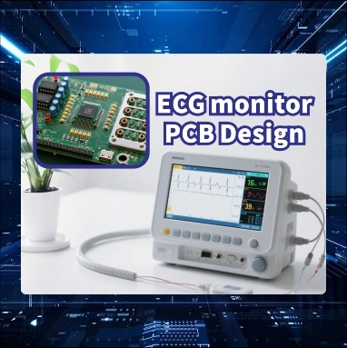
Patient monitors, ECG/EEG modules, portable ultrasound scanners, pulse oximeters, infusion pumps, electronic thermometers, blood pressure monitors, glucose meters, hearing aids, handheld diagnostic tools, medical imaging devices, endoscope control units, wearable health trackers, dental equipment, and sterilization system controllers.

How We Help:

  • Low-noise analog/digital mixed-signal design

  • Isolation and grounding optimization for patient safety

  • Biocompatible materials and moisture protection

  • Traceability documentation and IPC Class 3 compliance

Signal integrity at the speed of data.
We support the design of high-speed and RF PCBs used in telecommunication infrastructure, data centers, and networking devices.

Typical Applications:
5G base stations, RF transceiver modules, network switches, routers, optical transceivers, antennas, signal amplifiers, repeaters, VoIP gateways, satellite communication units, modems, network interface cards, PoE injectors, and telecommunication test instruments.

How We Help:

  • Controlled-impedance multi-layer design (10G–100G)

  • Low-loss materials: Rogers, Taconic, Megtron, PTFE

  • Crosstalk and reflection optimization

  • SI/PI simulation and stack-up optimization

Stable, rugged, and maintainable — engineered for 24/7 operation.
We design PCBs for industrial automation systems requiring high durability, wide temperature range, and EMI immunity.

Typical Applications:
PLCs, motion controllers, servo driver boards, motor control PCBs, inverter power modules, sensor interface boards, temperature controllers, industrial IoT gateways, HMI panels, power supply boards, relay modules, data acquisition boards, smart meters, robotic control systems, and energy management systems.

How We Help:

  • High-current and wide-temperature PCB layout

  • Isolation and filtering design for industrial noise

  • Thick-copper and conformal coating options

  • DFM/DFT for high-reliability production

Why IWDF PCB Design Services is Trusted By 1000+ Global Clients

We are more than just designers – we are your engineering partner.

pcb assembly

IWDF PCB design services go beyond just schematics

We help you bring ideas to life and avoid costly pitfalls with our manufacturing-ready layouts and engineering support.
IWDF PCB Design Services

Experience That Delivers

With 20+ years in PCB design and 500+ successful projects, we have the hands-on experience to handle everything from compact IoT boards to complex multilayer systems, making us a partner you can trust.
IWDF Solutions PCB Factory

Expert Team, No Outsourcing

Our in-house engineers average 8+ years of experience. We don’t outsource critical tasks to freelancers or third parties, ensuring full control, consistency, and confidentiality throughout your project.
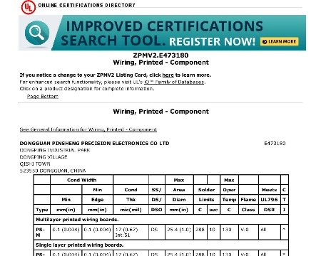
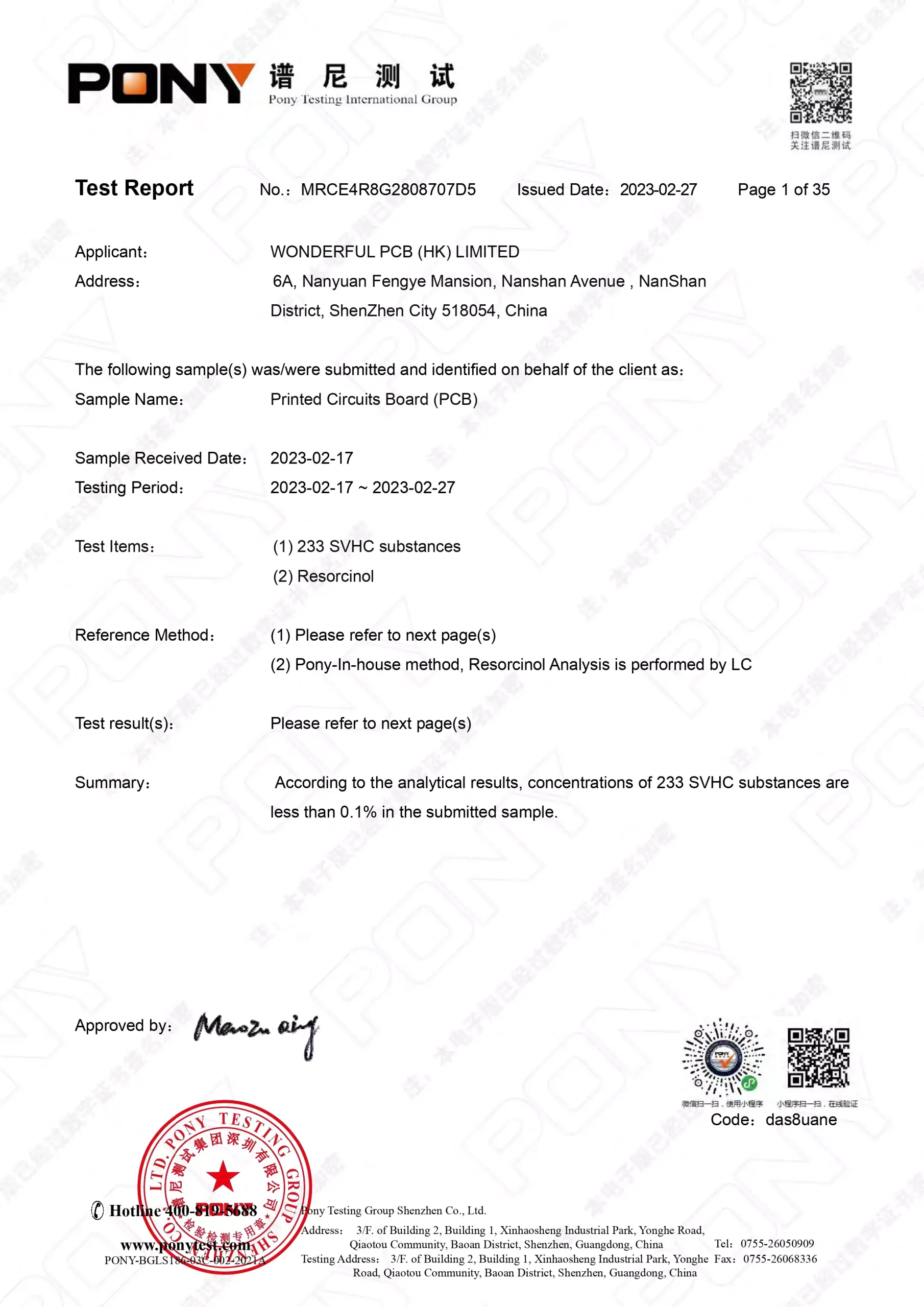
UL Certificate

Certified Quality Assurance

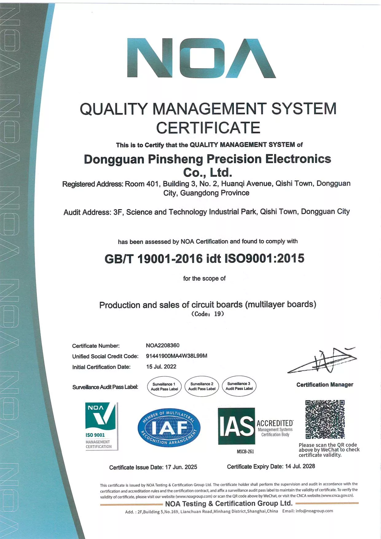
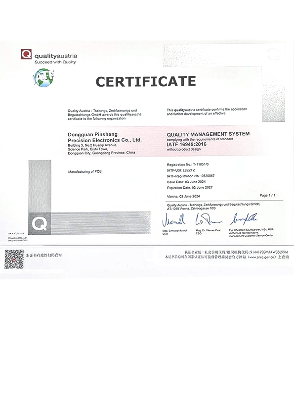
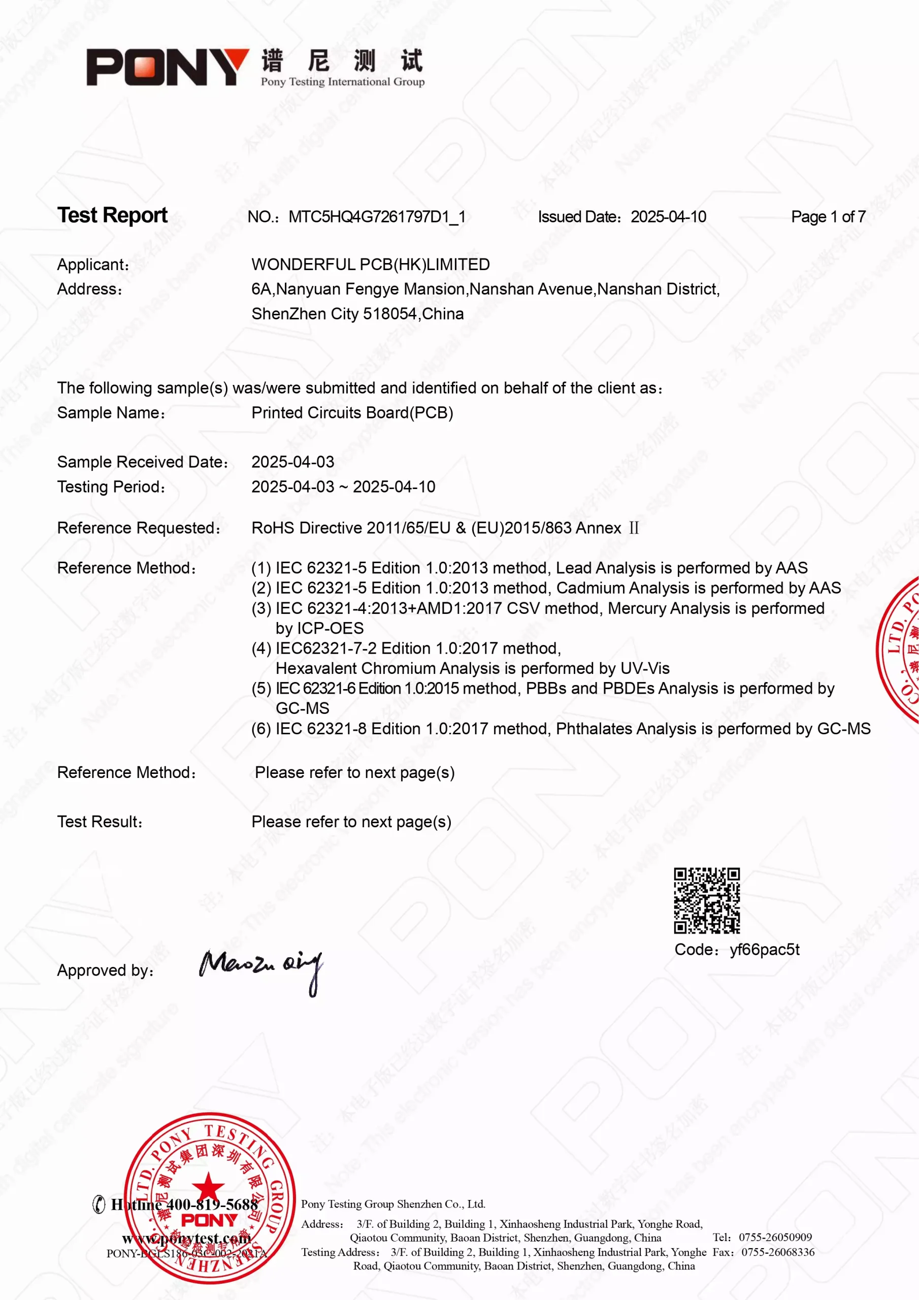
ISO9001:2015, UL, RoHS, IATF16949 (Automotive), ISO13485 (Medical), and REACH compliant.
Confidentiality Guaranteed

Confidentiality Guaranteed

NDAs and strict data handling ensure your IP is fully protected.
Global Support

Responsive Global Support

We provide 24/7 real-time engineering consultation in English, including schematic reviews and DFM (Design for Manufacturability) guidance.

Testimonials

You guys did exactly what you said you'd do — fast, clean, production-ready layouts. No drama, no delays. That’s why we came back for the second project​
Laura M
Laura M
Product Manager, MedCircuit Devices
Honestly, we were expecting at least one revision round, but your team nailed it on the first try. How? Witchcraft? Or just really solid engineering? Either way, we’re impressed — and our boss thinks we’re geniuses now.
Dylan
Dylan
Co-Founder, TinyBots Tech
What I appreciated most was your engineers’ attention to detail. You didn’t just follow our schematic — you challenged a few decisions and suggested better routing strategies. That saved us a lot of trouble in manufacturing. It’s rare to find a design partner who thinks like a factory​
Michael T
Michael T
Senior Engineer, Automation Systems Inc.

Certificates

We meet international standards to ensure your projects are safe, stable, and ready for any industry.

F.A.Q.

To provide an accurate quote, we typically require:
-Schematic diagrams or design files
-Bill of Materials (BOM)
-Mechanical constraints or enclosure details
-Specific design requirements (e.g., impedance control, layer count)
-Target production volume and timeline

We support Altium Designer, CAD, or PADS, Allegro, and Eagle. Deliverables include Gerber, BOM, and Pick & Place files.

Yes, we offer expedited services, with turnaround times based on project complexity. Feel free to contact us to discuss the details.

Turnaround times vary based on project complexity. Simple designs may take a few days, while more complex, multi-layer boards could require several weeks. We provide estimated timelines after reviewing your project requirements.

Absolutely. Every project includes DFM/DFA review to avoid costly manufacturing errors.

Absolutely. Our engineers are experienced in designing high-speed and RF PCB, incorporating best practices for signal integrity, impedance matching, and minimizing electromagnetic interference.

Absolutely. We can assist at any stage of your design process, whether you’re starting from scratch or need support refining an existing schematic.

Yes. We specialize in layout improvements, size reduction, DFM enhancements, and thermal/signal integrity optimization.

We’ve designed PCB for IoT, automotive, consumer electronics, medical, industrial control, and robotics applications.

We offer end-to-end solutions, including prototyping and full-scale production. Our manufacturing facilities are equipped to handle various production volumes with high-quality standards.
 Absolutely. We sign NDAs, and our facility complies with strict IP protection protocols.

 You can start by contacting us through our website, WhatsApp number, or directly via email. Provide us with your project details, and our team will guide you through the next steps, including quoting and project planning.

Ready to Start Your PCB Design Project?

— Let us help you design a PCB that powers your innovation.

Scroll to Top