

Your power board is burning traces, warping after assembly, or failing under load — most of these failures are not assembly defects. They start at the design stage, and the root cause is almost always the same: the copper weight, design rules, and manufacturing process were never matched to each other from the beginning.
That is exactly what heavy copper PCB design requires you to get right. A heavy copper PCB is a board where one or more copper layers carry 3 oz/ft² (105 µm) or more. It delivers higher current capacity, better thermal performance, and longer service life than a standard board — but only when the trace geometry, via sizing, layer stackup, and fabrication process are all specified and controlled together.

This guide is written for engineers, hardware leads, and procurement managers who need to make real decisions: how to design a heavy copper board correctly, what to specify in a fabrication drawing, and what to ask a factory before placing an order. The goal is not to explain what a heavy copper PCB is — it is to help you avoid the most common and costly mistakes when designing and sourcing one.
What Exactly Is a Heavy Copper PCB?
A heavy copper PCB is defined by a copper weight of 3 oz/ft² or above on at least one layer. When the copper weight reaches 20 oz/ft², the PCB is considered an extreme copper PCB. Standard boards use 1 oz copper. Moving to 3 oz is not a minor upgrade — it requires different etch chemistry, different press parameters, and different DFM rules across the entire design.
When does your design actually need heavy copper?
Heavy copper is the right choice when one or more of these conditions apply:
- Sustained high current — Any trace carrying more than 8–10 A continuously on a 1 oz board will overheat unless the trace is impractically wide. Heavy copper solves this within the same footprint.
- Aggressive thermal cycling — Boards that switch power on and off repeatedly develop mechanical fatigue at via barrels, solder joints, and copper-to-laminate interfaces. Thicker copper resists this better.
- High ambient temperature — If your board operates near or above 85°C, standard 1 oz copper planes cannot dissipate heat fast enough on their own.
- Mechanical stress environments — Aerospace, automotive, and industrial equipment expose boards to vibration, shock, and pressure. Heavy copper improves the structural integrity of the board itself.
If your design only has a few moderate-current power rails alongside signal routing, a mixed-copper approach — heavy copper on inner power planes with 1 oz outer layers — often delivers better cost and manufacturability than all-layer heavy copper. This is a stackup decision your manufacturer should help you evaluate before you commit. A factory that never raises this question is optimizing for order value, not for your design outcome.
Which Copper Weight Is Right for Your Current Requirements?
Engineers often over-specify copper weight because they don’t have a fast reference. This adds cost without adding reliability. Under-specifying is worse — it causes field failures that are much harder to trace back to the original design decision.
Use IPC-2152 as your primary reference for current capacity in heavy copper design. Do not rely on IPC-2221 alone — it was calibrated for thinner copper and can give results 20–30% off at 4 oz and above. The table below is based on IPC-2152 at a 10°C temperature rise for external traces with no forced airflow. For internal traces, derate by 15–25%.
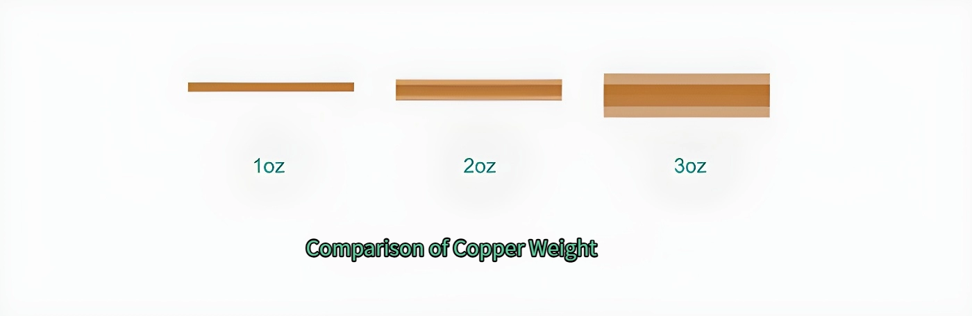
Copper Weight vs. Current Capacity Reference Table
| Copper Weight | Thickness | 50 mil trace | 100 mil trace | 200 mil trace | Primary Use Case |
|---|---|---|---|---|---|
| 1 oz | 35 µm | ~2.5 A | ~4.5 A | ~8.0 A | Signal, low power |
| 2 oz | 70 µm | ~3.5 A | ~6.3 A | ~11 A | Medium power distribution |
| 3 oz | 105 µm | ~5.0 A | ~9.0 A | ~16 A | High-current power planes |
| 4 oz | 140 µm | ~6.5 A | ~12 A | ~21 A | BMS, motor drives |
| 6 oz | 210 µm | ~9.0 A | ~16 A | ~29 A | Solar inverters, converters |
| 8 oz | 280 µm | ~11 A | ~21 A | ~38 A | Railway, heavy industrial |
| 10 oz | 350 µm | ~14 A | ~26 A | ~47 A | Defense, high-power RF |
| 20 oz+ | 700 µm+ | — | 60–200+ A | — | Extreme power, PCB busbars |
Once you know your worst-case sustained current per trace, add a 20% width margin on top of the IPC-2152 minimum. Heavy copper etching tolerances are wider than standard copper, and a trace designed at the exact minimum may come back underwidth after fabrication. If your current requirement exceeds 50 A on a single path, distribute the load across multiple parallel traces or planes rather than sizing one trace for the full load — this also helps significantly with heat spreading.
With the copper weight chosen, the next step is designing the board correctly. This is where most heavy copper failures are seeded.
How Do You Design a Heavy Copper PCB Correctly?
Picking the right copper weight is the easy part. Designing the traces, vias, and layer stack correctly is where the real engineering work begins — and where most problems originate. The four areas below each affect a different failure mode. They are not independent. A spacing error interacts with an etch profile problem. A via sizing error interacts with a thermal cycling problem. Design them together.
Trace Width and Spacing: Why Heavy Copper Changes Both Rules
Trace width and spacing are inseparable in heavy copper design. Standard PCB rules assume 4–6 mil minimum spacing for 1 oz copper. For heavy copper PCB design, the minimum must increase by at least 20–30%. There are two concrete reasons.
Reason one: etch profile. Etching heavy copper does not produce a vertical trace wall. The etchant works laterally as well as vertically, creating a trapezoidal cross-section — the trace base is wider than the top. At 6 oz copper with a 10 mil drawn spacing, the actual base-to-base gap after etching may be only 7–8 mils. Your EDA tool does not show this. Your factory’s etch compensation values do.
Reason two: thermal and arc risk. High-current traces generate heat and, at elevated voltages, concentrate the electric field between adjacent conductors. For voltages above 50V, IPC-2221 Table 6-1 specifies mandatory minimum clearances that go well beyond standard PCB design rules.

| Copper Weight | Min Spacing (Low Voltage) | Min Spacing (50–150V) | Note |
|---|---|---|---|
| 1–2 oz | 4–6 mils | Per IPC-2221 | Standard rules apply |
| 3–4 oz | 8–10 mils | Add 30% to IPC-2221 | Etch compensation required |
| 6 oz | 12–15 mils | Verify with fabricator | Trapezoidal etch is significant |
| 8–10 oz | 15–20 mils | Custom DFM required | Factory must provide specific rules |
Before you finalize any spacing-critical layout at 4 oz or above, ask your fabricator for their copper-weight-specific etch compensation values. A qualified factory gives you specific numbers. A factory that gives you generic answers is not controlling its etch process.
Via Design: Sizing and Plating for Thermal Cycling Survival
Via failures in heavy copper boards are among the most common field failure modes — and among the most preventable. Standard via rules do not work here, and substituting them is a direct path to cracked barrel failures in service.
Standard PCBs use 8–12 mil drill diameters with 0.5–1 mil of plated copper in the barrel. In a heavy copper board, that via carries more current, sees higher thermal stress, and endures more mechanical cycling than a standard via ever would. A thin barrel cracks. Once it cracks, resistance rises, heat increases, and the board fails — often months after field deployment, which is the worst time to discover a design rule violation.
Minimum drill diameter: Use 30 mils (0.75 mm) as the standard minimum for all power and thermal vias. For vias carrying more than 10 A, use 40 mils or larger.
Via plating thickness: IPC-6012 Class 2 requires a minimum of 0.8 mils of copper in via barrels. For heavy copper boards, this is not sufficient. Specify 2 mils minimum for power vias and 3 mils for thermal vias in your fabrication drawing. Ask your factory for a microsection coupon showing barrel wall thickness from a recent heavy copper production lot — a specification claim is not the same as evidence.
Via arrays instead of single oversized vias: For currents above 30 A, use 6–12 vias in parallel rather than a single large via. Arrays distribute both current and thermal stress across a wider area, which improves reliability under cyclic thermal load significantly. A single large via concentrates all stress at one point.
Via-in-pad with copper fill and cap: For thermal vias under BGA or power component pads, specify copper-filled and capped vias. This eliminates solder wicking into the via barrel — which causes solder starvation at the joint — and creates a solid thermal conduction path through the board. In heavy copper thermal designs, this is standard practice, not an upgrade.
Annular ring: Increase minimum annular ring to 8 mils for heavy copper boards. Drill registration tolerances scale with board thickness, and heavy copper boards are thicker. A 5 mil annular ring that works on a standard 4-layer board becomes marginal on a heavy copper design.
Layer Stackup: How to Build a Board That Won’t Warp
Board warpage is the number-one yield killer in heavy copper PCB manufacturing. A warped board fails SMT placement, causes solder joint opens, and can warp further during reflow — destroying the full assembly. The cause is almost always a design decision made before the board went into production.
Warpage in heavy copper boards comes from copper density imbalance between layers. When one side of the board carries more copper mass than the other, the two sides contract at different rates during lamination cooling. This creates a bimetal-like bending effect that stays in the board permanently.
Rule one: Mirror your copper density. Keep the copper coverage difference between mirror layers below 10–15%. On a 4-layer board, L1 mirrors L4 and L2 mirrors L3. If your power layer on L2 is 6 oz with 70% copper coverage, L3 should carry similar copper mass. A solid ground plane pour achieves this balance even if L3 has no other routing.
Rule two: Use copper thieving in sparse areas. In any layer region with low copper density, add a cross-hatched copper pour connected to ground. This reduces CTE imbalance without introducing parasitic capacitance problems. It is standard DFM practice at any factory experienced with heavy copper.
Rule three: Symmetric material construction around the board centerline. Cores and prepreg must be placed symmetrically — equal thicknesses and equal material types on both sides of the center. An asymmetric material stack amplifies warpage under heat, regardless of how balanced the copper is.
Rule four: Match prepreg resin content to copper topography. Standard prepreg may not fill the gaps between heavy copper traces adequately during lamination, creating voids in the dielectric. Use high-resin-content prepreg (106 or 1080 glass styles) adjacent to heavy copper layers. Tell your factory the copper weight and approximate coverage percentage per layer and ask them to confirm their prepreg selection. If they do not model lamination flow before production, they are guessing.
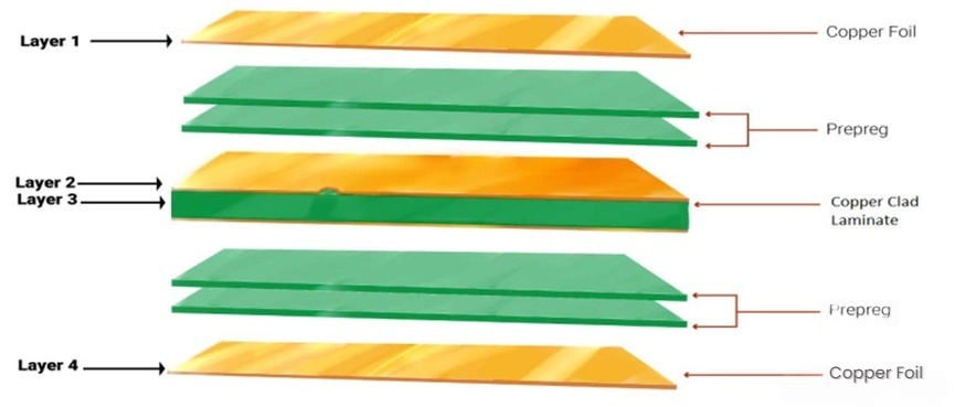
The table below shows a practical 4-layer stackup for a mixed heavy copper design. This structure is stable, manufacturable, and keeps CTE forces in balance:
| Layer | Function | Copper Weight | Coverage Target |
|---|---|---|---|
| L1 (Top) | Components + signal | 1 oz | ~40–50% |
| L2 (Inner 1) | Power plane | 6 oz | ~70% |
| L3 (Inner 2) | Ground plane | 6 oz | ~70% |
| L4 (Bottom) | Components + signal | 1 oz | ~40–50% |
DFM Details That Get Missed Before Production
After trace, via, and stackup decisions are complete, four DFM points are consistently missed in heavy copper designs — and that cause problems in production if not caught in the review stage.
Soldermask specification: The surface of a heavy copper board is not flat. Thick copper traces create raised topography that soldermask must bridge. If the mask is too thin at trace edges, it cracks during thermal cycling and exposes copper. Specify LPI (Liquid Photo Imageable) soldermask — not epoxy ink — for all heavy copper boards. LPI flows into the topography better and bonds more reliably.
Soldermask opening sizing: Expand SMD pad openings by 2–4 mils per side to account for the registration offset introduced by the thicker substrate surface. Standard solder mask expansion values calibrated for 1 oz boards can cause mask-over-pad encroachment on heavy copper designs.
Silkscreen: Silkscreen lines over heavy copper areas can appear uneven due to surface height variation. Use inkjet or LPI silkscreen rather than epoxy ink for consistent adhesion and legible markings.
Edge-to-copper clearance: Maintain a minimum of 20 mils from board edge to any copper feature. Heavy copper near the routed edge is prone to burring and micro-delamination during routing, which creates solder bridges and short-circuit risk after assembly.

What Manufacturing Challenges Should You Verify Before Ordering?
Understanding manufacturing difficulties is not background reading — it is a practical tool for evaluating factories. The questions below directly follow from the four main heavy copper manufacturing challenges. Ask them before you send Gerbers.
On etching: “What is your etch compensation specification for 4 oz and 6 oz copper, and what is your trace width tolerance?” A factory with real process control gives you specific numbers. A factory without it gives you a range so wide it’s meaningless.
On via plating: “Do you use pulse plating for high-aspect-ratio vias, and can you provide a microsection from a recent heavy copper lot?” Pulse plating forces more uniform copper distribution inside the via barrel. DC plating alone produces thinner copper in the center of the barrel, which is exactly where barrel cracks initiate.
On lamination: “How do you select prepreg for heavy copper stackups, and do you run a lamination flow model before production?” Voids form when resin flow is insufficient around heavy copper features during pressing. A factory that models this before production prevents it. A factory that doesn’t find out during inspection — or you find out in the field.
On soldermask: “Do you use LPI soldermask for heavy copper boards, and what is your mask thickness specification over heavy copper traces?” This one question alone separates factories that have built heavy copper before from those that are treating it like a standard order.
If a factory cannot answer these questions with specific, documented responses, the risk of a defective first article is high — regardless of price.
Which Industries Use Heavy Copper PCBs and What Does That Mean for Your Sourcing?
This matters because a factory that produces consumer-grade heavy copper boards may not have the process controls your application requires. The table below maps industries to requirements:
| Industry | Typical Application | Key Requirement | Copper Weight Range |
|---|---|---|---|
| EV / Automotive | BMS, onboard charger, traction inverter | –40°C to +125°C cycling, vibration | 3–6 oz |
| Renewable Energy | Solar inverter, wind converter | Long outdoor service life, sustained high current | 4–10 oz |
| Industrial Automation | VFD, servo amplifier, welding equipment | High surge current, uptime-critical | 3–8 oz |
| Aerospace / Defense | Avionics, radar, satellite hardware | MIL-spec reliability, IPC-6012 Class 3 | 4–10 oz |
| Medical | MRI power supply, laser surgery module | Stable power, regulatory documentation | 3–6 oz |
| High-Power LED | Stadium, horticulture, automotive lighting | Thermal uniformity across array | 2–4 oz |
If your application falls in aerospace, defense, or medical, specify IPC-6012 Class 3 compliance in your purchase order. Most standard factories only offer Class 2. Class 3 requires tighter controls, additional inspection steps, and traceability records. Not every factory in China can deliver this — and the ones that can will tell you so clearly.
The global heavy copper PCB market is currently valued at approximately USD 2.71 billion and is projected to reach USD 5.64 billion by 2035 at a CAGR of 8.49%, driven primarily by EV electrification and grid-scale energy storage expansion.
How Do You Evaluate a Heavy Copper PCB Manufacturer Without Making a Costly Mistake?
China produces the majority of global heavy copper PCBs, but the capability varies enormously. A factory that quotes you a price without asking about stackup symmetry, etch compensation, or via plating specification is not equipped for this work — regardless of what its website claims.
Manufacturer Evaluation Checklist
| Question | Minimum Acceptable Answer |
|---|---|
| Max copper weight offered? | 6 oz minimum; 10–20 oz for advanced projects |
| Min trace/space at 6 oz? | Specific DFM rule (e.g., 10 mil trace / 12 mil space) |
| Via plating thickness? | 2 mils minimum, confirmed by microsection coupon |
| Pulse plating capability? | Yes, for high-aspect-ratio vias |
| Prepreg selection for heavy copper? | High-resin content (106/1080 glass), matched per stackup |
| IPC-6012 Class 3? | Available with documentation for critical applications |
| Certifications? | ISO 9001:2015; UL Recognition for US/EU market entry |
| DFM review before production? | Yes, written feedback, no extra charge |
| Inspection methods? | AOI + X-ray + microsection coupon per production lot |
Engineering Support Is as Important as Fabrication Capability
A factory that only accepts Gerber files and processes them without review is a print shop, not a manufacturing partner. For heavy copper boards, DFM feedback before production is what separates a clean first article from an expensive respin. Corrections caught at the DFM stage cost nothing. The same corrections after a failed prototype cost you schedule, budget, and confidence.
If your design is not yet final, a factory with in-house heavy copper PCB design capability is a real advantage. A manufacturer that designs and fabricates the same board brings direct knowledge of what their own process requires. There is no information loss between the designer and the factory floor.
What Can IWDF Solutions Do for Your Heavy Copper PCB Project?
IWDF Solutions is a PCB engineering and manufacturing company based in Shenzhen, China. We provide heavy copper PCB design, fabrication, PCB reverse engineering, PCB cloning, and full PCBA production as a one-stop service. You can bring us a concept, a schematic, a reference board, or a finished design file — and receive assembled, tested boards without managing multiple vendors.
IWDF Solutions Heavy Copper PCB Capabilities
| Capability | Specification |
|---|---|
| Copper weight range | 1 oz to 20 oz (extreme copper on request) |
| Layer count | Up to 32 layers |
| Min trace / space (1 oz) | 4 mil / 4 mil |
| Min trace / space (6 oz) | 8 mil / 10 mil |
| Substrates available | FR-4, High-Tg FR-4 (Tg170), Halogen-Free, Polyimide, Rogers, MCPCB |
| IPC compliance | IPC-6012 Class 2 and Class 3 |
| Certifications | ISO 9001:2015, UL Recognition |
| Inspection | AOI, X-ray, microsection coupon per production lot |
| DFM review | Included with every order — written report before production |
| Prototype turnaround | 5–7 business days |
| Production turnaround | 15–20 business days including final QC |
Every order includes a written DFM review before production. We do not charge separately for this — it is part of how we prevent problems before they become your problem. All engineering communication is in English, and every project has a dedicated engineering contact, not a rotating sales inbox.
If you have a design ready, send us your Gerber files, stackup with copper weight per layer, via specifications, substrate material, and target quantity. We will return a DFM report and full quotation within 24 hours.
Frequently Asked Questions About Heavy Copper PCB Design
What is the difference between a heavy copper PCB and a standard PCB?
A standard PCB uses 1 oz copper (35 µm). A heavy copper PCB uses 3 oz or more on at least one layer. The difference is not just thickness — heavy copper requires different etch chemistry, different lamination parameters, different via sizing, and different DFM rules throughout. The manufacturing process is fundamentally more demanding at every stage.
How much current can a 3 oz heavy copper trace carry?
At 100 mils (2.54 mm) trace width, 3 oz copper carries approximately 9 A at a 10°C temperature rise (IPC-2152, external trace, no forced airflow). At 200 mils, the same copper weight handles approximately 16 A. Always base your calculation on your actual temperature rise budget, and derate by 15–25% for internal traces.
What is the minimum via size for a heavy copper PCB design?
30 mils (0.75 mm) drill diameter is the recommended minimum for power and thermal vias. Specify plating thickness explicitly in your fabrication drawing: 2 mils minimum for power vias, 3 mils for thermal vias. Ask your factory for a microsection sample — a specification written in a datasheet is not the same as confirmed process output.
Why do heavy copper PCBs warp during manufacturing?
Warpage is caused by a copper density imbalance between mirror layers. When one side of the board carries more copper mass, the two sides contract at different rates during post-lamination cooling. The solution is to keep copper coverage differences between mirror layers below 10–15% and use symmetric core and prepreg construction around the board centerline.
Can I mix copper weights on different layers?
Yes, and this is often the best approach. A common design uses 6 oz on inner power planes and 1 oz on outer signal layers. This reduces cost compared to all-layer heavy copper and keeps outer layers easier to work with during assembly. When mixing weights, always model the stackup for CTE symmetry. Your fabricator should confirm this before lamination.
What substrate should I use for heavy copper boards in high-temperature applications?
Standard FR-4 has a Tg of 130–140°C. If your board operates above 85°C ambient or goes through repeated thermal cycling, use high-Tg FR-4 (Tg 170°C) at minimum. For sustained operation above 150°C or aerospace applications, polyimide is the appropriate substrate. It costs more, but it is the only option that survives long-term in those conditions.
What files do I need to send to get a quote for heavy copper PCB fabrication?
Send: Gerber files (or design requirements if you need design services), a stackup with copper weight per layer, board dimensions and layer count, via drill sizes and plating specifications, substrate material, quantity, and turnaround requirement. If you also need IPC-6012 Class 3 compliance or specific testing, include that in the initial request. The more complete your information, the faster your quote and the more accurate the DFM feedback.
How do I know if a Chinese PCB factory is actually capable of heavy copper production?
Ask for their DFM design rules at 4 oz and 6 oz — specific trace/space minimums and etch compensation values, not a generic table. Ask for a microsection coupon from a recent heavy copper lot. Ask whether they use pulse plating for via barrels. Ask how they select prepreg for heavy copper stackups. A factory with real process knowledge answers all of these questions with specific, documented responses. A factory without it answers with marketing language.

