

When you are selecting PCB design software, you are not just choosing a drawing tool. You are choosing the workflow, file formats, collaboration model, and even the long‑term manufacturability of your products. The right tool can speed up development and reduce risk, while the wrong one can create hidden costs, rework, and communication issues with your PCB manufacturer.
This guide walks through the main types of PCB design software tools, compares 17 popular options, and explains how to match them to your project, team, and budget. Helping you:
- Pick the right software if you’re new to PCB design.
- Compare tools if you’re an engineer or product manager.
- Evaluate a PCB design supplier’s expertise based on the tools they use.

What Is PCB Design Software?
PCB design software is a specialized computer program used to design the physical layout of printed circuit boards (PCBs). Think of it as the essential toolkit that turns an electrical circuit diagram into a precise, manufacturable blueprint for the actual board. Without it, creating reliable, complex electronics efficiently would be nearly impossible.
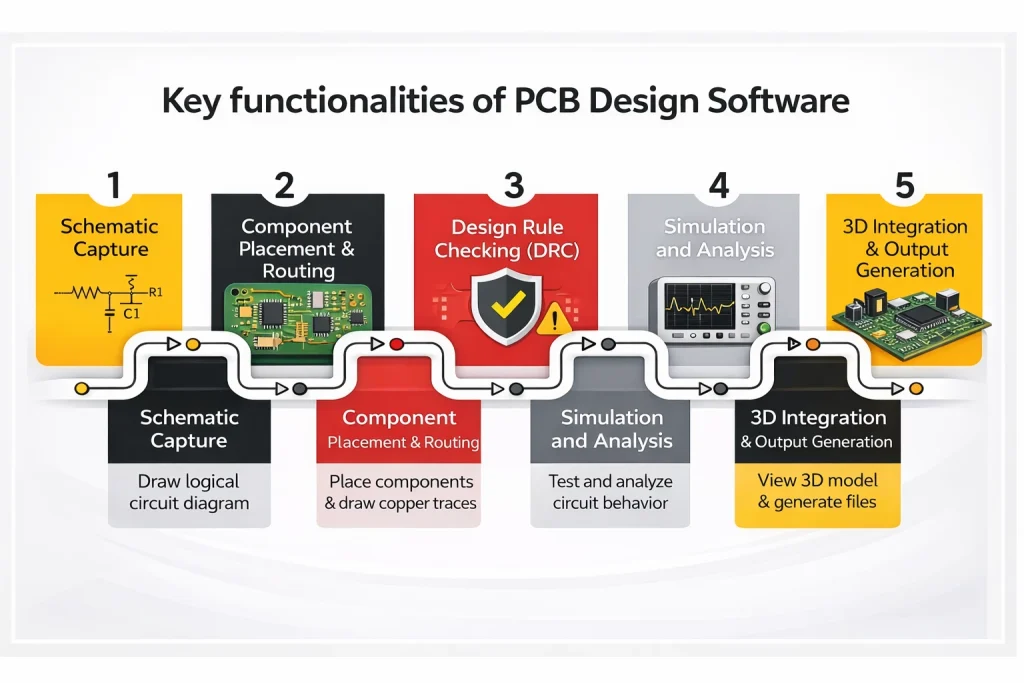
Core Functions and Why They Matter
- Schematic Capture: This is where you start, drawing the logical circuit diagram. The software provides a library of component symbols (like resistors, chips, and connectors) and intelligent tools to connect them, creating an error-free digital representation of your circuit’s connections.
- Component Placement & Routing: Once your schematic is ready, you move to the board layout. Here, you place the physical components and draw the copper traces that connect them. The software handles multi-layer boards and critical rules, such as ensuring traces are wide enough to carry the required current and that components aren’t placed too close together.
- Design Rule Checking (DRC): This is a crucial safeguard. You define a set of rules based on your manufacturer’s capabilities and your board’s electrical needs (e.g., minimum spacing between traces). The software constantly checks your layout against these rules, flagging violations before you send the design for fabrication, saving significant time and cost.
- Simulation and Analysis: Professional tools let you test your design virtually. You can simulate the circuit’s behavior to verify it works as intended, analyze how high-speed signals will travel, and check for potential overheating issues. This step dramatically increases the chance of a working board on the first try.
- 3D Integration and Output Generation: Modern software can show a realistic 3D model of your assembled PCB, allowing you to check for physical conflicts with enclosures or other components. Finally, it generates the standard industry files (like Gerber and drill files) needed by PCB manufacturers to build your board.
Why Use Dedicated Software Instead of Manual Methods?
For a beginner, the key advantage is structured error prevention. Manually designing a PCB, even a simple one, is prone to overlooked mistakes—a misplaced connection, a trace that’s too thin, or components that clash. These errors are cheap to fix on your computer but expensive and time-consuming once the board is manufactured.
PCB design software guides you through a correct-by-construction process. It keeps your schematic and layout synchronized, enforces physical and electrical rules in real time, and provides the tools to verify your decisions. This structured approach is what enables both hobbyists and professional engineers to successfully build everything from simple gadgets to sophisticated commercial devices.
Why should you care about PCB design software?
Almost every electronic device—from smart home gadgets to medical equipment—relies on a printed circuit board (PCB). The performance and reliability of the final product depend not only on the components used but also on the quality of the PCB design. And that quality is shaped largely by the software used to create it.
For buyers, entrepreneurs, or project managers, understanding the software landscape helps you:
- Communicate clearly with designers or suppliers.
- Gauge a team’s experience level (e.g., advanced tools often indicate professional expertise).
- Avoid delays, budget overruns, or manufacturing issues.
If you’re working with a PCB design supplier—especially when evaluating partners from different regions—one practical tip is to ask what software they use. The answer can reveal their workflow compatibility, skill level, and ability to handle complex projects.
In short, knowing the tools of the trade helps ensure your project stays on time, within budget, and optimized for production—whether you’re designing yourself or choosing someone to do it for you.
Types of PCB design software tools
Before diving into individual products, it helps to group PCB tools into a few broad categories.
- Professional desktop EDA suites
- Examples: Altium Designer, Cadence Allegro, OrCAD, PADS Professional, Xpedition, Zuken CR‑8000.
- Focused on complex, multi‑layer, high‑speed and high‑reliability boards for industrial, automotive, aerospace, and telecom applications.
- Free and open‑source tools
- Examples: KiCad, Altium CircuitMaker, EasyEDA (free tier), Fritzing, LibrePCB.
- Ideal for learning, prototyping, and budget‑constrained teams; capabilities have grown significantly in recent years.
- Cloud‑based and collaborative platforms
- Examples: Altium 365 (with Altium Designer and CircuitMaker), EasyEDA, Upverter, Autodesk Fusion (electronics).
- Designed for distributed teams, browser‑based access, and integrated data management.
- Education and entry‑level tools
- Examples: Fritzing, PCB Wizard, and some simplified online editors.
- Emphasize ease of use over advanced constraints or high‑speed features.
The right category depends on your project maturity, budget, and whether you are designing once or building a long‑term hardware product portfolio.
Overview table: 17 PCB design software tools
The table below summarizes the 17 tools covered in this guide so you can quickly see who they are best for.
| Tool | Primary positioning | Target users | Typical complexity | Deployment |
|---|---|---|---|---|
| Altium Designer | High‑end all‑rounder | Professional teams, SMEs, enterprises | Medium to very complex boards | Desktop + Altium 365 cloud |
| Cadence Allegro PCB Designer | Enterprise high‑speed / dense | Hobbyists, startups, and engineers | Very complex, high‑speed, high‑layer | Desktop, enterprise data mgmt |
| OrCAD PCB Designer | Professional mid‑to‑high | SMEs, professional designers | Medium to complex | Desktop |
| Siemens Xpedition | Enterprise advanced design | Tier‑1 OEMs, automotive, aerospace | Very complex, multi‑board | Desktop + enterprise mgmt |
| PADS Professional | Professional mainstream | SMEs, OEMs | Medium to complex | Desktop |
| Zuken CR‑8000 | Enterprise advanced | Automotive, industrial, telecom | Complex, system‑level | Desktop + data mgmt |
| Autodesk Eagle | SMB / prosumer | Makers, small businesses | Simple to medium | Desktop (now within Fusion) |
| Autodesk Fusion (Electronics) | Integrated MCAD+ECAD | Product teams needing 3D | Medium complexity, mech‑heavy | Cloud‑connected desktop |
| KiCad EDA | Free open‑source | Hobbyists, startups, engineers | Simple to moderately complex | Desktop, multi‑platform |
| EasyEDA | Cloud and free‑friendly | Students, startups, makers | Simple to moderately complex | Browser‑based + desktop |
| Altium CircuitMaker | Free community tool | Makers, open hardware | Simple to medium | Desktop + Altium 365 personal space |
| DipTrace | Affordable professional | SMBs, advanced hobbyists | Simple to medium | Desktop |
| Proteus Design Suite | PCB + simulation | Education, embedded teams | Simple to medium | Desktop |
| Upverter | Cloud collaborative | Startups, remote teams | Simple to medium | Browser‑based |
| Fritzing | Learning and prototyping | Students, makers | Very simple proto boards | Desktop |
| LibrePCB | Open‑source alternative | Open‑source enthusiasts | Simple boards | Desktop |
| PCB Wizard | Educational | Schools, training | Simple educational designs | Desktop |
This list covers a broad spectrum from free to high‑end enterprise tools, so you can see where you fit today and where you may want to be in the future.
Detailed Profiles of 17 PCB Design Software Tools
For each tool below, the structure is consistent to facilitate easier comparison: a brief history, positioning, key features, typical use cases, pros and cons, and a high-level view of pricing and licensing.
1. Altium Designer

History:
Altium Designer is one of the most widely recognized PCB design software platforms in the world. Its roots go back to the late 1980s, when the software was originally released under the name Protel in Australia. Over time, it evolved into a comprehensive electronic design automation (EDA) suite and was rebranded as Altium Designer in 2001. With decades of continuous development, it has grown into a market leader used by engineers in aerospace, automotive, consumer electronics, and high-reliability industries. Unlike many open-source tools, Altium Designer has always positioned itself as a professional-grade platform, aiming to combine usability with advanced technical capabilities.
Key Features:
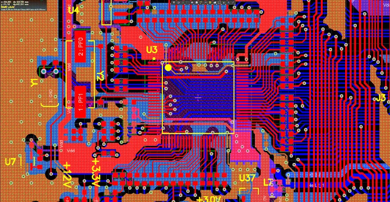
Altium Designer offers a broad set of tools for every stage of PCB design:
- Unified Design Environment – Schematic capture, PCB layout, simulation, and documentation are integrated in one platform.
- Advanced 3D Visualization – Engineers can view boards in realistic 3D, detect mechanical conflicts, and align with housing models.
- Design Rule Checks (DRC) – Built-in checks ensure compliance with manufacturing constraints such as clearance, impedance, and via sizes.
- Signal Integrity & Simulation – Tools for high-speed signal routing, differential pair design, and EMI/EMC validation.
- Collaboration Tools – Altium 365 allows cloud-based teamwork, version control, and real-time design reviews.
- Extensive Component Libraries – Prebuilt parts databases with footprints and simulation models.
- Multi-board Assembly – Supports system-level design with interconnected PCBs.
These features make Altium not just a PCB tool, but a complete ecosystem for electronic product development.


Pros:
- Industry-standard tool trusted by top companies.
- Powerful 3D modeling and real-time rule checks.
- Smooth integration between schematic and PCB layout.
- Extensive online libraries and cloud collaboration through Altium 365.
- Highly suitable for complex, multi-layer, high-speed designs.
Cons:
- High cost compared to most competitors.
- Steeper learning curve for beginners.
- Requires relatively strong hardware to run smoothly.
- Overkill for very small projects or hobbyist-level designs.
Pricing and licensing overview
Altium Designer is sold primarily as a subscription with options close to several thousand US dollars per year for full access; some regions also offer perpetual licenses with maintenance. Altium provides CircuitMaker as a free alternative for non‑commercial or community users, which shares some core technology
Best For
Altium Designer is best suited for:
- Professional engineers and enterprises need reliability for high-complexity designs.
- Industries where mistakes are costly (aerospace, medical devices, automotive).
- Teams working on multi-board or high-speed projects.
- Buyers evaluating suppliers: If a supplier uses Altium Designer, it usually signals a professional and experienced design team rather than a beginner.
2. Cadence Allegro PCB Designer
History:
Cadence Allegro originates from enterprise EDA workflows and is widely used in networking, telecom, and high‑performance computing. It is positioned as a top‑tier PCB layout tool for complex, high‑speed digital designs and large teams.

Key features
- Advanced constraint management for high‑speed interfaces (DDR, SerDes, high‑frequency links).
- Powerful interactive and auto‑routing options for dense boards with many BGAs.
- Integration with Cadence SI/PI and RF simulation tools.
- Enterprise data management, design reuse, and multi‑board support.
Typical use cases
- Backplanes, routers, telecom boards, high‑speed computing, and advanced industrial systems.
- Designs where signal integrity and timing closure are critical.
- Large organizations with established PCB design processes and strict documentation.

Pros
- Very strong high‑speed and constraint‑driven capabilities.
- Deep integration with other Cadence tools for full system design and analysis.
- Trusted in industries with strict compliance requirements.
Cons
- Steep learning curve, especially for beginners.
- High licensing and maintenance costs, often only justified for larger companies.
- Complex setup and workflows require disciplined teams.
Pricing and licensing overview
Allegro is sold as a professional enterprise tool with modular licensing; pricing is typically negotiated and not listed publicly, but it is at the high end of the market. It is usually justified when you have many safety‑critical or high‑speed designs and a dedicated PCB team
3. OrCAD PCB Designer
History:

OrCAD, short for Oregon + CAD, was first developed in the mid-1980s by a group of engineers in Oregon. It quickly gained traction as one of the earliest PC-based design automation tools, providing professional-level schematic capture and PCB layout capabilities at a time when most competitors required expensive workstations.
In the late 1990s, OrCAD was acquired by Cadence Design Systems, one of the largest electronic design automation (EDA) companies in the world. Since then, OrCAD has become part of the broader Cadence Allegro product family. Today, OrCAD is recognized as an industry-standard platform, especially valued in fields where reliability, compliance, and advanced simulation are critical—such as automotive electronics, aerospace, and telecommunications.
Key Features:
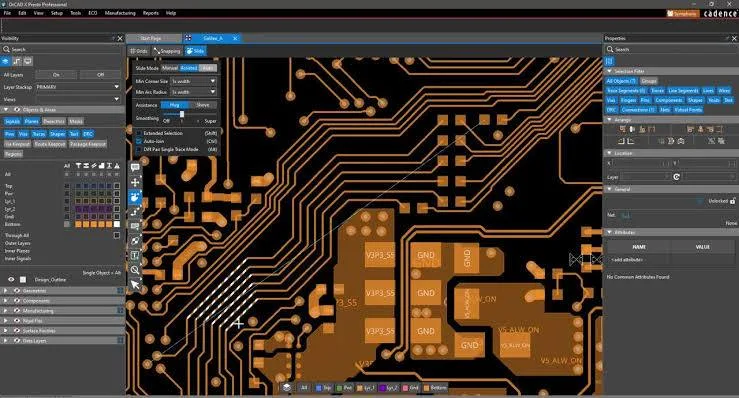
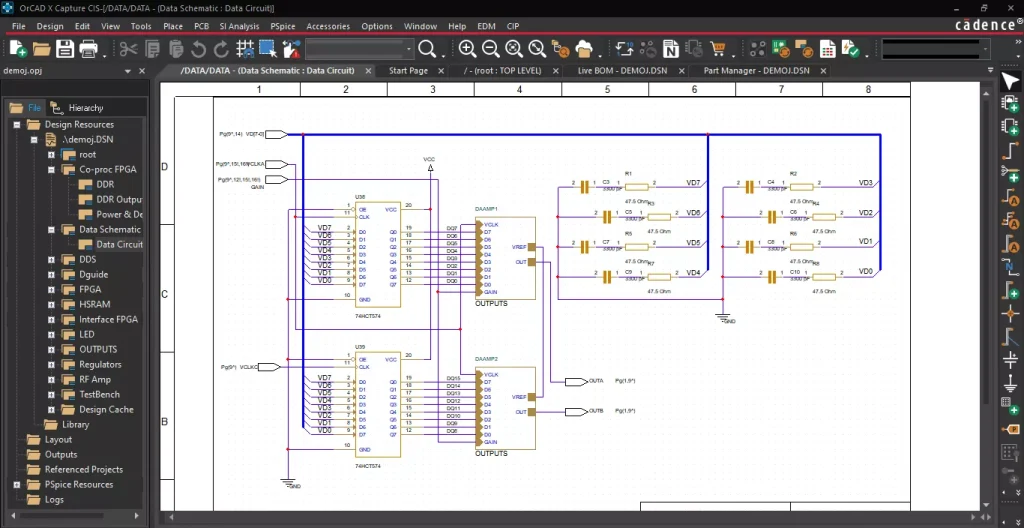
OrCAD offers a robust suite of features designed for professional PCB design:
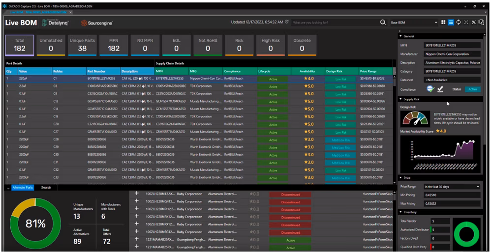
- Schematic Capture (OrCAD Capture) – One of the most widely used schematic editors in the industry, supporting complex hierarchical designs.
- PCB Layout (OrCAD PCB Designer) – Supports multi-layer boards, high-speed designs, and advanced constraint-driven layout.
- PSpice Simulation – Industry-leading analog and mixed-signal circuit simulation integrated directly into the workflow.
- Signal Integrity & Power Analysis – Ensures reliable performance in high-frequency and power-critical designs.
- Design for Manufacturability (DFM) – Tools to catch errors before production, reducing costly respins.
- Scalability – Can scale from OrCAD’s entry-level offerings up to Cadence Allegro for enterprise needs.
- Library & Database Management – Centralized component libraries with strong support for compliance and traceability.
This combination makes OrCAD not just a layout tool, but a comprehensive platform for design, simulation, and verification.

Pros:
- Trusted, industry-standard platform with decades of development.
- Extremely powerful simulation tools via PSpice.
- Constraint-driven design reduces errors in high-speed and complex boards.
- Strong integration with manufacturing processes and compliance standards.
- Scalable to Allegro for very large, enterprise-level projects.
Cons:
- Steeper learning curve than hobbyist-friendly tools like Eagle or EasyEDA.
- The user interface can feel dated compared to newer platforms.
- Higher cost than mid-range solutions.
- Requires strong hardware for optimal performance.
Pricing & Free Trial-Data
OrCAD is a commercial, subscription-based tool, though it comes in different tiers depending on the features required:
- OrCAD Capture CIS (schematic only) is available at a lower cost.
- OrCAD PCB Designer Standard: around $2,000–$2,500 per year.
- OrCAD PCB Designer Professional (with PSpice and advanced features): typically $3,500–$4,000+ per year.
- Free Trial: Cadence often provides a 30-day free trial with full features for evaluation.
- Student Versions: discounted licenses are available for universities and individual students.
While the cost is high, many companies see OrCAD as a long-term investment due to its reliability and advanced toolset.
Best For:
OrCAD is best suited for:
- Buyers evaluating suppliers: If a vendor uses OrCAD, it typically signals a professional-level design team with strong simulation and verification capabilities, though it also suggests a higher-cost operation compared to open-source or hobbyist tools.
- Professional engineering teams working on advanced electronics in industries like automotive, aerospace, defense, and telecom.
- Designs requiring deep simulation and verification, especially analog/mixed-signal circuits.
- Medium to large enterprises need scalable solutions with compliance support.
4. Siemens Xpedition
Brief history and positioning
Xpedition (originally from Mentor Graphics, now Siemens) is a flagship enterprise PCB design environment. It targets complex system‑level design, including multi‑board projects, automotive ECUs, and advanced industrial equipment.
Key features
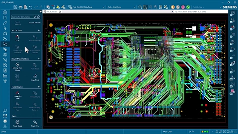
- Advanced constraint management, multi‑board design, and system‑level signal‑integrity integration.
- Sophisticated autorouting, via management, and design reuse for highly dense boards.
- Tight integration with Siemens PLM and mechanical tools for digital twin workflows.
- Strong DFM and DFA capabilities for collaboration with large manufacturing operations.
Typical use cases
- Automotive, aerospace, defense, and telecom where boards are large, dense, and safety‑critical.
- Organizations with full EDA departments and strict configuration management requirements.
Pros
- Excellent for very complex, multi‑board, and high‑reliability systems.
- Integrates well into enterprise PLM and model‑based engineering environments.
- Deep feature set for manufacturability and test planning.
Cons
- Very high cost and complexity.
- Not appropriate for small businesses, startups, or beginners.
- Requires significant training and process definition.
Pricing and licensing overview
Xpedition is negotiated on an enterprise basis, with costs that make sense only for large organizations with many users and high design volume. It is rarely the first tool you choose, butit may be your destination when your company scales
5. PADS Professional

History:
PADS was originally developed in the early 1980s by Personal Automated Design Solutions (PADS Software, Inc.) as one of the very first PCB design tools for personal computers. At that time, PCB design was dominated by workstation-class systems, so PADS played a key role in bringing professional EDA tools to desktop PCs.
In 2001, Mentor Graphics acquired PADS and expanded its capabilities, positioning it as a mid-range solution in the Mentor product portfolio—less complex than Xpedition (Mentor’s enterprise tool) but more powerful than low-cost alternatives. After Siemens acquired Mentor Graphics in 2017, PADS became part of the Siemens EDA suite, further integrating with advanced simulation, manufacturing, and digital twin technologies.
Today, PADS is recognized as a professional-grade PCB design tool particularly suited for small to medium design teams that need advanced features without the heavy enterprise complexity (or cost) of Xpedition.
Key Features:
- PADS offers a full-featured design environment with a strong emphasis on professional engineering workflows:
- Schematic Capture (PADS Logic) – A powerful schematic editor supporting hierarchical design and cross-probing with PCB layout.
- PCB Layout (PADS Layout) – Handles high-speed digital, analog, and mixed-signal designs with support for multi-layer boards.
- Signal Integrity Analysis – Integrated simulation tools for high-speed signals, ensuring reliable performance.
- Thermal & Power Analysis – Helps identify potential heat issues and optimize power delivery.
- Design for Manufacturability (DFM) Tools – Built-in checks to ensure boards are fabrication-ready.
- Component & Library Management – Centralized system with supplier links for BOM management.
- 3D Visualization – Board-level 3D modeling and mechanical verification.
- Integration with Siemens EDA Ecosystem – Smooth upgrade path to Xpedition for larger projects.
- PADS strikes a balance: advanced enough for professional use but lighter and more approachable than enterprise solutions.
Pros:
- Professional-grade capabilities for high-speed and complex designs.
- Strong simulation tools (signal integrity, thermal, and power analysis).
- Scalable—users can move from PADS to Xpedition as project needs grow.
- Backed by Siemens, ensuring continuous development and industry relevance.
- Trusted in many industries, making it a safe choice for suppliers.
Cons:
- Learning curve is steeper than mid-range tools like Eagle or DipTrace.
- More expensive than hobbyist- and startup-focused software.
- Interface can feel less modern compared to Altium Designer.
- Smaller community than open-source tools like KiCad.
Pricing & Free Trial-Data
PADS is a commercial tool, priced in the professional range but more affordable than enterprise suites:
- PADS Standard: Entry-level, focusing on schematic capture and basic PCB layout.
- PADS Standard Plus: Adds advanced features like signal integrity and thermal analysis.
- PADS Professional: The full package with advanced simulation, 3D modeling, and enterprise-level collaboration.
- Pricing typically starts around $5,000 for a perpetual license (varies based on modules and options).
- Subscription models are also available for teams that prefer lower upfront costs.
- Free Trial: Siemens usually offers a 30-day free trial of PADS Professional.
- Student Versions: Discounted or free academic licenses available through Siemens’ academic program.
Best For:
PADS is best suited for:
- Buyers evaluating suppliers: If a vendor uses PADS, it usually signals a professional team with strong industry practices, often handling mid-to-high complexity projects with attention to simulation and manufacturability.
- Professional engineers and small-to-mid design teams that require advanced features without jumping to full enterprise platforms.
- Companies are designing high-speed digital or analog circuits where signal integrity is critical.
- Organizations seeking scalability—PADS provides a natural upgrade path into Xpedition for very large projects.
6. Cadstar (Zuken CR‑8000)

History:
Cadstar is a PCB design solution from Zuken, a Japanese company founded in 1976, well-known in the EDA and ECAD/MCAD integration market. Unlike newer tools that emerged for hobbyists or startups, Zuken positioned Cadstar as a professional-grade PCB tool serving industrial electronics, automotive, aerospace, and telecom sectors.
Zuken has a strong global presence, especially in Europe and Asia, and has become a serious competitor to Altium, Mentor Graphics (now Siemens), and Cadence. While Cadstar itself is one of Zuken’s mid-tier products, its technology underpins Zuken’s high-end enterprise solutions like CR-8000, which are used by major corporations worldwide. This makes Cadstar both accessible for smaller design teams and scalable for large companies.
Key Features:
Cadstar provides a comprehensive set of PCB design and verification tools:
- Schematic Capture – Intuitive design entry with hierarchical schematic support.
- PCB Layout – Supports up to multi-layer boards, advanced routing, and manufacturing checks.
- High-Speed Design Tools – Constraint-driven design for signal integrity, differential pair routing, and length tuning.
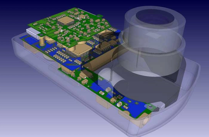
- 3D PCB Design & Verification – Integrated 3D viewing with MCAD data import/export.
- Simulation – SI (signal integrity) and EMC (electromagnetic compatibility) checks.
- Component Libraries – Extensive part libraries with easy management tools.
- Design Rule Check (DRC) & Manufacturing Outputs – Ensures designs are production-ready with Gerber, ODB++, and IPC standard exports.
- Scalability to CR-8000 – Cadstar projects can be migrated to Zuken’s enterprise system, making it a future-proof option.
Pros:
- Trusted by industries with mission-critical applications (automotive, aerospace, medical).
- Strong signal integrity and EMC simulation features.
- Professional-grade tool with scalability to enterprise-level platforms.
- Good balance between cost and advanced features compared to Altium/OrCAD.
- Backed by Zuken’s decades of engineering expertise and global support network.
Cons:
- Less known among hobbyists and small teams (a smaller online community compared to KiCad or EasyEDA).
- Interface feels more “traditional” compared to newer cloud-first tools.
- Learning curve can be steep for beginners.
- Not as widely adopted in the U.S. market compared to Altium or OrCAD.
- Pricing is less transparent—requires direct sales engagement.
Pricing & Free Trial-Data
Zuken does not publicly disclose Cadstar pricing, but it generally sits in the mid-range professional category:
- Academic Licenses: Discounted versions available for universities and research institutions.
- Perpetual License: Estimated $3,000–$6,000, depending on modules.
- Subscription Model: Available with annual maintenance and support.
- Free Trial: A demo or evaluation license can be requested directly from Zuken.
Best For:
Cadstar is best suited for:
- Medium-to-large design teams in industries requiring high reliability and compliance.
- Professional engineers who need advanced features like signal integrity analysis.
- Organizations planning scalability from small projects into enterprise-level Zuken solutions (CR-8000).
- Buyers evaluating suppliers: If a supplier uses Cadstar, it usually signals an established, professional engineering team with strong industry focus, particularly in regulated sectors like automotive or aerospace.
7. Autodesk Eagle

History:
EAGLE, which stands for Easily Applicable Graphical Layout Editor, was created in the late 1980s by CadSoft Computer GmbH in Germany. It quickly became a favorite among hobbyists and small companies due to its balance of affordability and functionality. Autodesk acquired Eagle in 2016, integrating it into their design ecosystem and eventually merging it with Fusion 360 to provide a unified platform for mechanical and electronic design. Today, Eagle exists as the electronics design module within Fusion 360, offering PCB design alongside mechanical CAD, simulation, and product lifecycle tools. This shift reflects Autodesk’s strategy of enabling full electromechanical co-design, making it easier for engineers to integrate PCBs into complex product assemblies.

Key Features:
Eagle is particularly strong for small to medium-scale designs and rapid prototyping:
- Schematic Capture & PCB Layout – Supports multi-sheet schematics and PCBs with up to 16 layers.
- Extensive Component Libraries – Direct integration with supplier libraries (Digi-Key, Mouser, etc.) for ready-to-use parts.
- Auto-router – Automated routing tool for speeding up board layout (though often refined manually by engineers).
- Design Rule Checks (DRC) – Ensures designs meet electrical and manufacturing constraints.
- SPICE Simulation – Enables basic analog and mixed-signal circuit analysis.
- Fusion 360 Integration – 3D CAD and PCB layout coexist in one environment, improving mechanical-electrical collaboration.
- Community Add-ons – Strong third-party ecosystem with scripts and ULPs (User Language Programs) for automation and customization.
This mix of flexibility and integration makes Eagle especially attractive to makers, startups, and teams that value rapid iteration.


Pros:
- Seamless integration with Fusion 360 for electromechanical projects.
- Wide adoption in the maker and hobbyist community.
- Large library support and direct supplier integration.
- Affordable subscription compared to Altium or OrCAD.
- Cloud-based collaboration with Autodesk’s ecosystem.
Cons:
- Autodesk has officially phased Eagle out as a standalone tool; it now requires Fusion 360.
- Feature set is less advanced than Altium, OrCAD, or Mentor for enterprise-level projects.
- Auto-router is helpful but often not optimal for high-speed or complex designs.
- Some long-time users resisted the shift to subscription-based licensing.
Pricing & Free Trial-Data
Since Eagle is now part of Fusion 360, its pricing is tied to Autodesk’s subscription model:
- Fusion 360 Personal (Free for hobbyists, limited features).
- Fusion 360 Standard: around $60/month or $495/year, includes Eagle functionality.
- Fusion 360 for Startups: Free for qualifying startups making less than $100,000 annually.
- Free Trial: Autodesk typically offers a 30-day free trial of Fusion 360 with full functionality.
This pricing structure makes Eagle more accessible than high-end platforms, though less flexible than free open-source solutions like KiCad.
Best For:
Autodesk Eagle is well-suited for:
- Buyers evaluating suppliers: If a design house uses Eagle/Fusion 360, it typically indicates a modern workflow with good mechanical-electrical integration, though not necessarily geared toward extremely high-end, complex boards.
- Hobbyists and makers designing small PCBs, especially when paired with Fusion 360 for 3D modeling.
- Startups and small businesses need an affordable, professional-grade tool for IoT, wearables, or consumer electronics.
- Educators and students are looking for an industry-recognized but accessible software platform.
8. Autodesk Fusion 360 (Electronics)

History:
Fusion 360 was launched by Autodesk in 2013 as a cloud-based mechanical CAD (MCAD) platform. It quickly became popular among product designers, engineers, and makers for its modern interface, affordability, and cloud collaboration features.
In 2016, Autodesk acquired Eagle (Easily Applicable Graphical Layout Editor), one of the most widely used PCB design tools at the time. Eagle was then integrated into Fusion 360, evolving into Fusion 360 Electronics, a seamless environment where mechanical and electronic design coexist.
Today, Fusion 360 is positioned as a unified platform for product development, combining mechanical design (CAD), electronic design (EDA/PCB), simulation, and manufacturing (CAM) in one ecosystem. It is especially attractive to startups and interdisciplinary teams who need mechanical + electronic design integration.
Key Features:
Fusion 360 offers a cross-domain toolset that bridges MCAD and ECAD:
- Schematic Capture (Fusion 360 Electronics) – Derived from Eagle, supports hierarchical design, cross-probing, and large component libraries.
- PCB Layout – Handles multi-layer designs, autorouting, and detailed design rules.
- MCAD-ECAD Integration – Real-time syncing between 3D mechanical and PCB design, avoiding mechanical fit issues.
- 3D PCB Visualization – Full 3D board previews inside the mechanical model, ensuring accurate housing and enclosure fitting.
- Component Libraries – Vast Eagle + Fusion 360 libraries, with managed components linked to suppliers.
- Simulation Tools – Signal integrity, thermal, and basic circuit simulation included.
- Cloud Collaboration – Real-time collaboration, version control, and project sharing.
- CAM Integration – Export to manufacturing workflows, CNC machining, and additive manufacturing directly inside Fusion 360.
- Extensive Add-Ons – API and plug-ins for extended workflows.
Fusion 360’s unique strength is the tight coupling between mechanical and electronic domains, reducing the back-and-forth that traditionally occurs between PCB designers and mechanical engineers.

Pros:
- Unified platform for MCAD + ECAD + CAM = one-stop solution.
- Based on Eagle, so many users find the learning curve manageable.
- Cloud-based collaboration, version history, and team sharing.
- Affordable compared to separate CAD and PCB tools.
- Direct manufacturing workflows for both PCBs and mechanical parts.
Cons:
- Requires stable internet for full functionality (cloud-heavy).
- PCB toolset, while powerful, is less advanced than Altium or OrCAD for enterprise-scale boards.
- Some Eagle users felt the transition into Fusion 360 introduced complexity.
- Subscription-only model—no perpetual license option.
- Less appealing for companies with strict data/IP security policies due to cloud reliance.
Pricing & Free Trial-Data
Fusion 360 uses Autodesk’s subscription model:
- Standard Subscription: ~$70/month or ~$545/year for the full package (includes PCB + CAD + CAM).
- Free for Hobbyists/Students: Non-commercial license available, limited features but still powerful.
- Startup License: Free 3-year license for eligible small businesses/startups (under revenue threshold).
- Free Trial: 30-day free trial for new users.
This pricing strategy makes Fusion 360 one of the most cost-effective ways to access both MCAD and ECAD in a single package.
Best For:
Fusion 360 is best suited for:
- Startups and product teams that need seamless mechanical + electrical integration.
- Makers and hobbyists are taking advantage of the free or discounted versions.
- Small-to-mid-sized companies building complete products (housing + PCB + simulation + prototyping).
- Buyers evaluating suppliers: If a supplier uses Fusion 360, it often signals a flexible, interdisciplinary team comfortable with both mechanical and electronic design, making them especially strong in product-level design rather than just PCB layout.
9. KiCad EDA
History:
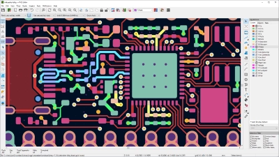
KiCad is one of the most popular open-source PCB design tools, first developed in the early 1990s by Jean-Pierre Charras, a French engineer. Unlike commercial platforms that rely on licensing fees, KiCad is fully free and community-driven. Over time, it has gained significant institutional support, most notably from CERN (the European Organization for Nuclear Research), which now contributes heavily to its ongoing development. This support has transformed KiCad from a hobbyist tool into a serious contender in the professional space. Today, it’s trusted by startups, educational institutions, and even some professional design teams seeking an affordable alternative to high-cost EDA suites.
Key Features:
Despite being free, KiCad offers a surprisingly powerful feature set:
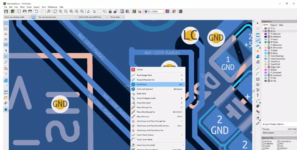
- Schematic Capture & PCB Layout – Intuitive interface for creating circuit diagrams and routing boards up to 32 layers.
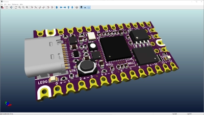
- 3D Viewer – Realistic visualization of components and board geometry, helpful for mechanical fit checks.
- Design Rule Checks (DRC) – Automatic verification of clearance, trace width, and manufacturing rules.
- Large Component Libraries – Community-driven symbol and footprint libraries, plus integration with services like Digi-Key and Octopart.
- SPICE Simulation – Basic circuit simulation via Ngspice for testing electrical behavior.
- Cross-Platform Support – Runs on Windows, macOS, and Linux.
- File Export Compatibility – Supports Gerber, STEP, and other industry-standard formats for manufacturer compatibility.
Recent updates have improved the user interface, library management, and multi-board project handling, making KiCad more competitive with commercial tools.

Pros:
- Completely free and open-source (no licensing fees).
- Strong support from CERN and an active global community.
- Frequent updates and continual improvement.
- Capable of handling professional-level multi-layer boards.
- Excellent choice for students, hobbyists, and startups with limited budgets.
Cons:
- Interface and workflows can feel less polished than commercial tools.
- No official customer support—reliance on community forums and documentation.
- Fewer advanced features (e.g., signal integrity analysis, enterprise collaboration tools).
- Component libraries, while vast, sometimes require extra cleanup or verification.
Pricing & Free Trial-Data
KiCad is 100% free—no license fees, no subscription, and no feature restrictions.
- Open-source GPL license, meaning users can modify or extend the software as they wish.
- Free for commercial, academic, and personal use.
- Supported by donations and sponsorships (CERN, companies, and the user community).
Unlike most commercial tools, there is no trial period—all features are always accessible.
Best For:
KiCad is ideal for:
- Buyers evaluating suppliers: If a design partner uses KiCad, it doesn’t automatically mean they are inexperienced—many skilled engineers use it—but it may indicate a leaner, cost-sensitive design process compared to premium tools like Altium.
- Students and educators are looking for a zero-cost yet capable PCB design solution.
- Hobbyists and makers are prototyping electronics projects at home.
- Startups and small businesses need professional features without high software costs.
- Open-source hardware communities that value transparency and collaboration.
10. EasyEDA

History:
EasyEDA was launched in 2013 by a group of Chinese engineers who wanted to make PCB design more accessible to a global audience. Unlike traditional EDA tools that require heavy desktop installation and licensing, EasyEDA was created as a cloud-based platform. The goal was simple: remove the barriers of cost, software complexity, and installation hassles.
Over time, EasyEDA partnered with JLCPCB, one of the largest PCB manufacturers in the world, creating a unique workflow where users can design, simulate, and directly order PCBs from a single platform. This integration has made EasyEDA a go-to tool for hobbyists, students, and startups, while still gaining traction among professionals who need fast prototyping.
Key Features:
- EasyEDA combines simplicity with cloud-powered convenience:
- Web-Based & Cross-Platform – Runs in a browser, with desktop versions also available for offline work.
- Schematic Capture – User-friendly editor with a large online parts library.
- PCB Layout – Supports up to 6 layers (standard in most plans), autorouting, and manual routing options.
- Component Libraries – Direct link to LCSC’s massive online component catalog, reducing sourcing time.
- Simulation Tools – Basic SPICE-based simulation for circuit analysis.
- 3D View – Visualize boards in 3D with component placement previews.
- Cloud Collaboration – Share projects online, collaborate in real-time with team members.
- Seamless Manufacturing Integration – Direct export to JLCPCB for quick prototyping and production.
- Import/Export Options – Gerber files, JSON, and other standard formats supported.
- Its main strength lies in ease of use + integrated manufacturing—making it especially popular for rapid prototyping.


Pros:
- 100% free to use at the basic level.
- No installation needed—accessible from any device with internet access.
- Direct integration with JLCPCB for manufacturing saves time.
- Large online component library linked to real suppliers.
- Great for beginners thanks to the intuitive interface and tutorials.
- Real-time collaboration features for teams.
Cons:
- Not as powerful as enterprise tools like Altium or OrCAD for complex, high-speed designs.
- Limited to 6-layer boards in standard use.
- Heavy reliance on cloud can be a concern for teams with strict IP security requirements.
- Performance may lag with very large or highly complex designs.
- Vendor lock-in risk if relying heavily on JLCPCB integration.
Pricing & Free Trial-Data
EasyEDA follows a freemium model:
- Free Version – Most core features are available free, with project storage limits and some advanced features restricted.
- Professional/Enterprise Plans – Paid plans (around $5–$20/month) expand project storage, add collaboration features, and provide priority support.
- Manufacturing Integration – Users typically pay for PCB fabrication via JLCPCB, not for the software itself.
- Free Trial – Since the base tool is already free, no separate trial is needed.
This pricing makes EasyEDA one of the most cost-effective PCB design tools on the market.
Best For:
EasyEDA is best suited for:
- Buyers evaluating suppliers: If a supplier uses EasyEDA, it usually indicates a focus on low-to-mid complexity projects, rapid prototyping, and cost-efficiency. It may suggest a younger or leaner design team compared to firms using OrCAD, Altium, or PADS.
- Students and beginners are learning PCB design for the first time.
- Makers and hobbyists who want free and quick access to design + manufacturing.
- Startups need rapid prototyping at low cost.
- Distributed teams that want easy cloud-based collaboration.
11. Altium CircuitMaker
History and positioning
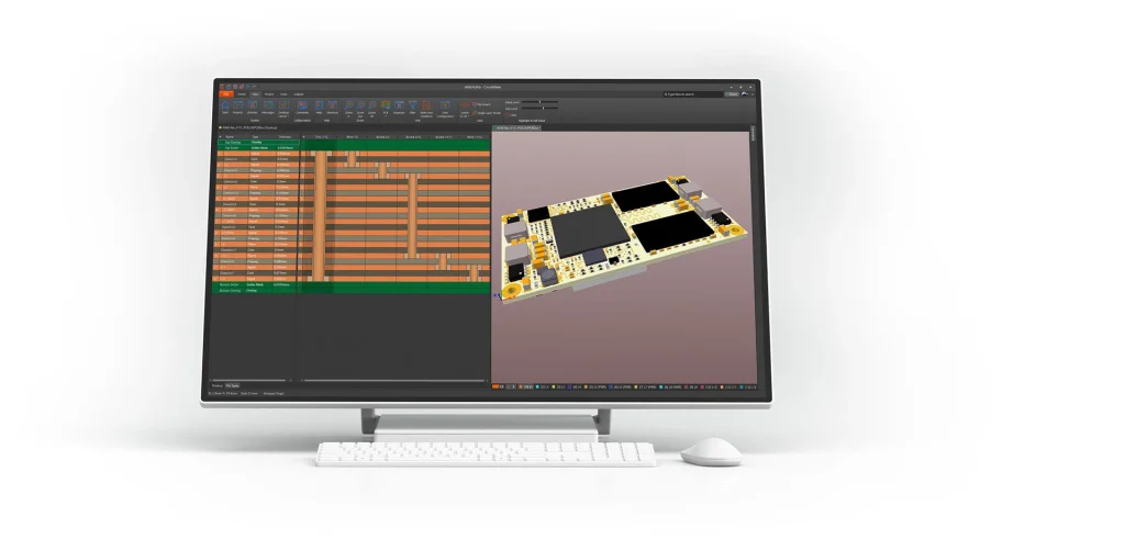
CircuitMaker is Altium’s free community‑driven PCB design tool for makers, students, and part‑time engineers. It shares a core technology base with Altium Designer and connects to Altium 365 for cloud storage.
Key features
- Desktop schematic and PCB design with a modern user interface.
- Cloud project storage in an Altium 365 personal space, with sharing and collaboration.
- Access to community‑driven libraries and design examples.
Typical use cases
- Individual designers and open‑source hardware projects.
- Students who want to learn an Altium‑like workflow without paying for a license.
Pros
- Free to use for individual and community projects.
- Good stepping stone to Altium Designer, as many concepts transfer directly.
- Cloud collaboration for review and sharing.
Cons
- Limited for closed, commercial projects because of its community‑oriented nature.
- Not suitable for confidential or sensitive designs.
Pricing and licensing overview
CircuitMaker is free; users are expected to store projects in the cloud and accept some community visibility depending on project settings.
12. DipTrace

History:
DipTrace was first developed in the early 2000s by Novarm Limited, a company based in Ukraine. Unlike legacy EDA tools that evolved over decades, DipTrace was designed from the start to be intuitive and accessible, lowering the barrier to entry for PCB design without sacrificing professional functionality. Over time, it has gained a steady following among small to mid-size companies, startups, and independent engineers who want a simpler alternative to heavyweight platforms like Altium or OrCAD.
Today, DipTrace is recognized for its clean interface, strong library support, and cost-effective licensing options, positioning it as a bridge between hobbyist tools (like Eagle or KiCad) and enterprise tools (like Altium).
Key Features:
DipTrace offers a full PCB design workflow with an emphasis on ease of use:
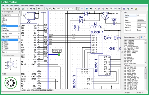
- Schematic Capture – Straightforward schematic editor with hierarchical design support.
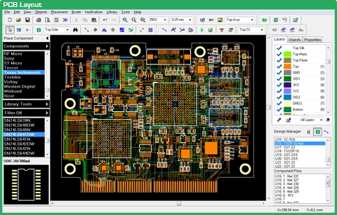
- PCB Layout – Supports up to 32 signal layers, 3D modeling, and flexible routing (manual + auto-router).
- Component & Pattern Libraries – Over 150,000 ready-to-use components plus library wizards for creating new parts.
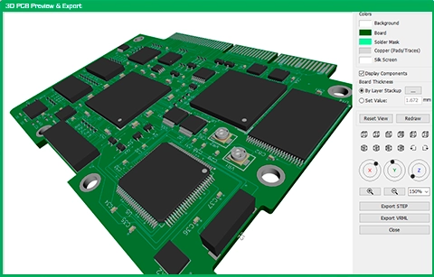
- 3D PCB Preview – Realistic visualization with export options for mechanical CAD software.
- Design Rule Check (DRC) – Ensures compliance with manufacturer constraints before fabrication.
- Import/Export – Supports Gerber, DXF, STEP, and other industry formats for manufacturer compatibility.
- Cross-Probing – Real-time synchronization between schematic and PCB layout.
- High-Speed Features – Differential pair routing, length tuning, and controlled impedance for signal integrity.
While not as advanced as Altium or OrCAD, DipTrace includes enough professional-grade tools to handle most small-to-medium complexity boards.

Pros:
- Intuitive and beginner-friendly interface compared to many EDA tools.
- Affordable licensing with flexible tiers for different users.
- Strong component libraries and good 3D visualization.
- Solid import/export compatibility with industry-standard formats.
- Differential pair routing and impedance control—features often missing in lower-cost tools.
Cons:
- Less powerful for extremely large, multi-board, or enterprise-level designs.
- Smaller user community compared to KiCad or Eagle.
- Fewer collaboration tools (no cloud-native system like Altium 365).
- Documentation and tutorials, while improving, are not as extensive as larger competitors.
Pricing & Free Trial–Data from 2025 Year
DipTrace offers one of the most flexible and affordable licensing models in the PCB software market:
- Free Version – Non-commercial, limited to 300 pins and 2 signal layers.
- Lite Edition – Around $75–$125, for small boards with limited pins/layers.
- Standard Edition – Around $350–$400, supports up to 1,000 pins and 4 signal layers.
- Extended Edition – Around $695–$750, for more complex boards with up to 10,000 pins.
- Full Edition – Around $1,200, with no limitations on board size or complexity.
- Free Trial – Fully functional 30-day trial available.
This tiered approach makes DipTrace accessible to hobbyists, freelancers, and small businesses, while still offering scalability for more advanced work.
Best For:
- Hobbyists and beginners who want an easy entry into PCB design without the steep learning curve.
- Freelancers and small businesses working on small to medium-complexity projects.
- Startups need professional features like impedance control at a lower cost.
- Educational institutions teaching PCB design with accessible, affordable tools.
- Buyers evaluating suppliers: If a supplier uses DipTrace, it may suggest a cost-conscious team focused on small-to-mid complexity designs, but not necessarily lacking in professionalism.
13. Proteus Design Suite

History:
Proteus was developed by Labcenter Electronics, a UK-based company, in the late 1980s. Originally designed as a simulation platform for microcontrollers and embedded systems, it gradually evolved into a full PCB design suite. What makes Proteus stand out is its ability to combine circuit simulation, microcontroller emulation, and PCB layout in one package.
Over the years, Proteus gained massive popularity in educational institutions and embedded systems developers, particularly in fields where simulation of microcontrollers (such as Arduino, PIC, ARM, or AVR) is as critical as designing the actual PCB. Today, Proteus remains one of the most widely used tools in universities and training centers, and is also embraced by embedded-focused startups and engineers.
Key Features:
Proteus integrates PCB design with powerful simulation capabilities:
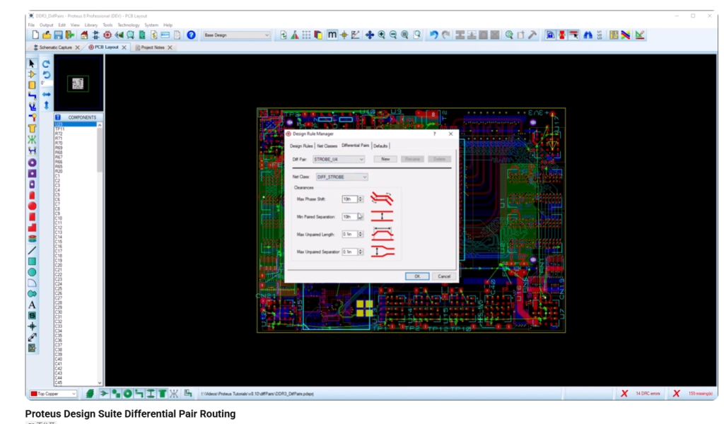
- Schematic Capture – Intuitive schematic editor with hierarchical design options.
- PCB Layout – Supports multi-layer boards, manual + autorouting, and design rule checks.
- Microcontroller Simulation – Unique ability to simulate MCUs like PIC, AVR, ARM Cortex-M, Arduino, STM32, and more.
- Embedded Co-Simulation – Runs real firmware (HEX/ELF files) within virtual circuits to test behavior before hardware fabrication.
- SPICE Simulation – Analog and digital circuit simulation for verification.
- 3D Visualization – Preview PCB design in 3D for inspection and mechanical integration.
- Integrated Libraries – Thousands of models for microcontrollers, sensors, and ICs, reducing design setup time.
- IoT Development Support – Recently added support for simulating IoT devices and communication modules.
Pros:
- Unique microcontroller and firmware simulation—rare among PCB tools.
- Highly popular in academia, making it easy to learn and adopt.
- Wide range of pre-built MCU libraries (Arduino, PIC, STM32, etc.).
- Saves time by debugging firmware + hardware in simulation before prototyping.
- Affordable compared to enterprise tools.
Cons:
- Less suited for very large, high-speed professional boards (where Altium or PADS excel).
- Community is smaller outside academia compared to open-source tools like KiCad.
- Interface feels less modern than cloud-first tools (e.g., EasyEDA).
- Limited collaboration tools compared to Altium 365 or Fusion 360 PCB.
Pricing & Free Trial-Data from 2025 Year
Proteus pricing is flexible and tier-based, depending on the feature set:
- Student & Academic Licenses – Substantially discounted, widely used in universities.
- Proteus PCB Design Starter Kit – ~$250–$300, basic PCB layout + schematic capture.
- Proteus PCB Design Level 2/3 – ~$1,000–$3,000, includes simulation and multi-layer support.
- Proteus Platinum – Comprehensive version with all libraries and modules included.
- Free Trial – 14-day evaluation available.
Best For:
Proteus is best suited for:
- Buyers evaluating suppliers: If a supplier uses Proteus, it usually indicates a strong focus on embedded systems, prototyping, and firmware-heavy projects—ideal for IoT or microcontroller-based products.
- Embedded systems developers who want to test firmware and hardware together.
- Educational institutions teaching microcontrollers, electronics, and PCB design.
- Hobbyists and students working on Arduino, PIC, or ARM-based projects.
14. Upverter
History and positioning
Upverter is one of the early cloud‑based PCB design tools, targeted at collaborative, hardware‑startup‑style workflows.

Key features
- Browser‑based schematic and PCB editor.
- Real‑time collaboration and shared component libraries.
- Emphasis on simple workflows and team visibility.
Typical use cases
- Distributed startup teams that need light, web‑based tools.
- Early‑stage prototypes and small production runs.
Pros
- No local installation required.
- Easy sharing and collaboration in a browser environment.
Cons
- Less feature‑rich than mature desktop tools.
- Cloud reliance may not match strict security policies.
Pricing and licensing overview
Upverter has historically offered free and paid tiers; details and integration with specific manufacturers evolve, so it is best treated as a flexible cloud option for lighter designs.
15. Fritzing
History and positioning
Fritzing was created to make electronics design accessible to designers, artists, and students with a breadboard‑style interface.

Key features
- Breadboard view for visual prototyping.
- Schematic and simple PCB layout.
- Simple interface aimed at non‑engineers.
Typical use cases
- Educational environments to introduce PCB concepts.
- Very simple breakout boards and small projects.

Pros
- Very easy for beginners and visual thinkers.
- Bridges the gap from breadboard to basic PCBs.
Cons
- Not suitable for complex, high‑reliability products.
- Libraries and outputs are more limited than mainstream tools.
Pricing and licensing overview
Fritzing is open‑source with paid downloadable builds or donations supporting development. It is best viewed as a teaching tool, not a full production EDA.
16. LibrePCB
History and positioning
LibrePCB is a newer open‑source PCB design project designed to be simple yet modern.

Key features
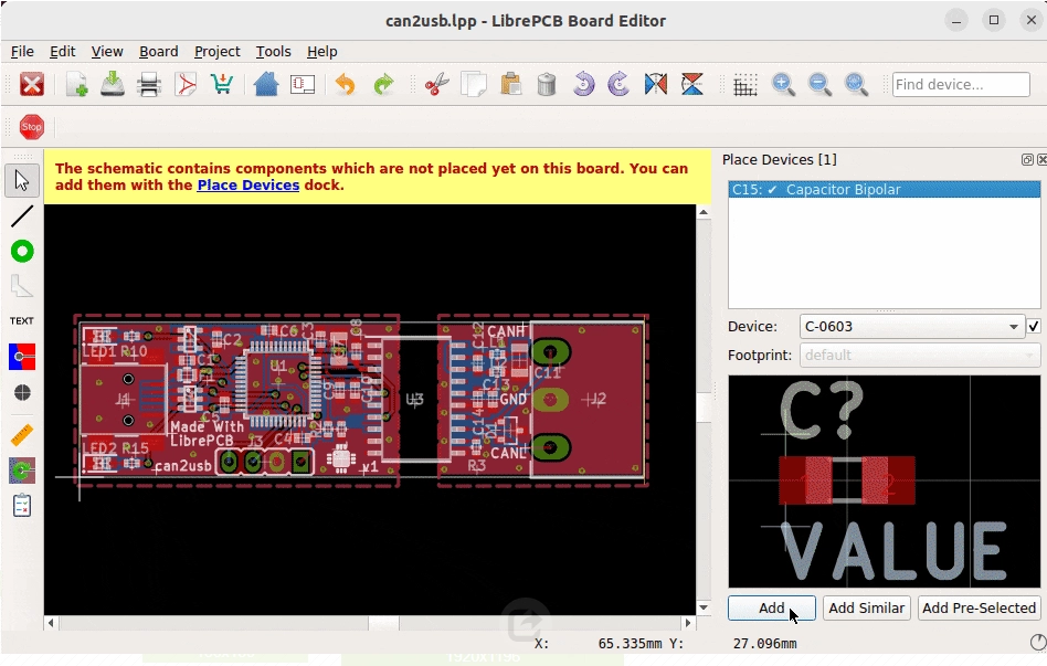
- Schematic and PCB layout with a clean user interface.
- Emphasis on straightforward library concepts and workflows.
Typical use cases
- Open‑source enthusiasts and hobbyists wanting a fully open toolchain.
- Simple product designs without extreme constraints.
Pros
- Open‑source and free to use.
- Modern design philosophy and active development.
Cons
- Smaller user community than KiCad; fewer tutorials and libraries.
- Not yet as feature‑complete for advanced designs.
Pricing and licensing overview
LibrePCB is free; costs are mainly your time and effort building libraries and processes.
17. PCB Wizard
Brief history and positioning
PCB Wizard is a long‑standing educational PCB design tool used in schools and basic electronics courses.

Key features
- Easy‑to‑use schematic and PCB editor focused on simple boards.
- Educational resources and templates for teaching.
Typical use cases
- School environments and introductory electronics classes.
- Very small, low‑complexity projects.
Pros
- Simple for newcomers and teachers.
- Quick way to introduce PCB design without overwhelming students.
Cons
- Not suitable for professional‑grade, complex products.
- Limited in terms of libraries, DFM, and advanced features.
Pricing and licensing overview
PCB Wizard is offered as commercial software with educational licensing; it is affordable for schools but not usually considered in professional tool evaluations.

How to Choose PCB Design Software for Your Industry?
Selecting PCB design software isn’t one-size-fits-all. The right tool depends heavily on your industry’s specific demands for reliability, regulation, cost, and performance. This guide breaks down the key requirements and tool considerations for major sectors.
1. Automotive Electronics: Built for Safety and Longevity
- The Core Challenge: Designing systems that must operate flawlessly for over a decade in harsh environments (under-hood heat, vibration, electrical noise) while meeting strict functional safety standards.
- What Drives Tool Choice: Compliance and reliability are non-negotiable. Your software must help you enforce rules automatically.
- Key Needs in a Tool:
- Functional Safety Workflows: Direct support for ISO 26262 and ASIL levels, ensuring systematic error prevention.
- Robust Simulation: Advanced signal integrity (for CAN/CAN FD/LIN buses) and thermal analysis are essential.
- Supply Chain Integration: Ability to manage and trace components qualified to automotive standards (e.g., AEC-Q100/200).
- Comprehensive Analysis: Built-in EMI/EMC checking to ensure operation despite ignition noise and meet regulatory limits.
- Typical Tools: Cadence Allegro is the entrenched standard for Tier 1 suppliers due to its deep analysis and compliance features. Zuken CR-8000 or Cadstar are strong alternatives, especially in Europe.
2. Aerospace & Defense: Extreme Environment Reliability
- The Core Challenge: Creating electronics that survive extreme temperature swings, cosmic radiation, and intense vibration, with full documentation for certification and traceability.
- What Drives Tool Choice: Traceability, rigorous change control, and support for military/aerospace-specific standards and components.
- Key Needs in a Tool:
- Certification Support: Features that aid in compliance with standards like DO-254 for airborne systems.
- Advanced Material & Component Libraries: Access to parts rated for military (MIL-SPEC) and extended temperature ranges.
- Change Management: Formal configuration and change control processes integrated into the design workflow.
- Specialized Analysis: Capabilities for modeling radiation effects and thermal cycling stress.
- Typical Tools: Cadence Allegro (with specialized packages) and Zuken CR-8000 dominate, as they are built to handle these complex, document-heavy processes.
3. Medical Devices: Regulation and Traceability
- The Core Challenge: Navigating stringent FDA or CE mark regulatory pathways, which require rigorous design controls, risk management, and full traceability of components and decisions.
- What Drives Tool Choice: Software that structures the design process to automatically generate the documentation needed for regulatory audits.
- Key Needs in a Tool:
- Design History Management: Strong version control and audit trails for every change.
- Documentation Workflow: Tools to manage design inputs, outputs, verification protocols, and risk analysis (per ISO 14971).
- Material Compliance: Features to track biocompatibility (ISO 10993) and sterilization compatibility of materials.
- Reliability Focus: Simulation tools for critical aspects like power integrity and thermal performance.
- Typical Tools: Altium Designer is popular for its strong documentation and collaboration features at a mid-range cost. Large firms may use Cadence Allegro for its high-reliability focus.
4. IoT & Wearables: Speed and Miniaturization
- The Core Challenge: Rapidly iterating on compact, cost-sensitive, battery-powered devices with integrated wireless connectivity.
- What Drives Tool Choice: Fast learning curve, quick turnaround from design to prototype, and tight integration with affordable, high-volume manufacturing.
- Key Needs in a Tool:
- Fast Prototyping: Cloud-based platforms that facilitate quick edits and sharing.
- Manufacturing Links: Direct connection to PCB fabricators and component suppliers (like JLCPCB/LCSC) for instant pricing and availability.
- Library Management: Large, pre-verified libraries for common microcontrollers, sensors, and wireless modules (Bluetooth, Wi-Fi, LoRa).
- Power Analysis: Basic tools to estimate battery life and optimize power rails.
- Typical Tools: EasyEDA (cloud-based, integrated manufacturing) and KiCad (free, powerful, open-source) are top choices. Fusion 360 is excellent for wearables requiring tight mechanical/PCB co-design.
5. Consumer Electronics: Cost and Volume Optimization
- The Core Challenge: Balancing performance and features with intense cost pressure and the need for designs that can be assembled reliably in volumes of hundreds of thousands.
- What Drives Tool Choice: Tools that provide deep supply chain intelligence, accurate cost forecasting, and Design for Manufacturability (DFM) feedback early in the process.
- Key Needs in a Tool:
- Cost Management: Real-time BOM costing and alternate component finders to hit target prices.
- DFM/DFA Integration: In-tool checks for panelization, solderability, and assembly machine compatibility to avoid costly factory line issues.
- Supply Chain Insights: Links to distributor databases to avoid obsolete or long-lead-time parts.
- Performance Analysis: Thermal and EMI simulation to prevent field failures and ensure compliance (FCC, CE).
- Typical Tools: Altium Designer is a market leader for its comprehensive DFM and supply chain features. Fusion 360 offers a good feature/cost balance for many companies.
6. High-Frequency & RF: Signal Integrity is Everything
- The Core Challenge: Preserving the integrity of very fast or high-frequency signals (for 5G, radar, satellite) where the PCB layout itself becomes a critical component of the circuit.
- What Drives Tool Choice: Advanced simulation and modeling capabilities that treat PCB traces as transmission lines, not simple connections.
- Key Needs in a Tool:
- Integrated Simulation: 3D electromagnetic (EM) field solvers and signal/power integrity analysis built into the layout environment.
- Controlled Impedance Routing: Automated routing of traces to exact impedance values (e.g., 50Ω) with correct layer stackup management.
- Advanced Modeling: Accurate models for vias, connectors, and the effects of the board material (dielectric constant, loss tangent).
- Differential Pair Management: Precise control over differential trace routing, including length matching and spacing.
- Typical Tools: Cadence Allegro (with SI/PI options) and Keysight ADS are high-end standards. Altium with external simulators is a capable option for many RF projects.
Industry Selection Quick Reference
| ndustry | Core Challenge | Recommended Tool(s) | Key Features to Look For |
|---|---|---|---|
| Automotive | Functional safety & long-term reliability under extreme conditions. | Cadence Allegro | ISO 26262 compliance, advanced signal/thermal analysis. |
| Aerospace & Defense | Certification & traceability for extreme environments. | Cadence Allegro / Zuken CR-8000 | DO-254 support, rigorous configuration management. |
| Medical Devices | Regulatory approval (FDA) and risk management. | Altium Designer | Design control documentation, component traceability. |
| IoT / Wearables | Fast prototyping with tight cost & size constraints. | EasyEDA / KiCad | Cloud-based workflow, integrated manufacturing, component libraries. |
| Consumer Electronics | Cost optimization for high-volume production. | Altium Designer | Real-time BOM costing, DFM checks, supply chain tools. |
| High-Frequency / RF | Preserving signal integrity at multi-GHz speeds. | Cadence Allegro Sigrity | Integrated EM simulation, controlled impedance routing. |
Example comparison: free vs professional tools
To make the choice more concrete, the table below compares a few representative free and professional tools.
| Tool | Cost level | Best for | Strengths | Main limitations |
|---|---|---|---|---|
| KiCad | Free | Startups, hobbyists, pros on budget | No license cost, open files, strong community | No formal vendor support, some advanced constraints less mature |
| EasyEDA | Free/low | Beginners, students, fast prototypes | Browser‑based, easy to learn, fab integration | Cloud dependence, limited for very complex designs |
| CircuitMaker | Free | Makers, open hardware | Built on Altium tech, cloud collaboration | Community‑oriented, not ideal for confidential projects |
| Altium Designer | High | Professional teams, SMEs | Deep features, good balance of power and usability | High subscription cost, learning curve for beginners |
| OrCAD | Mid‑to‑high | Professional designers | Strong simulation and constraints | Interface complexity, commercial licensing |
| Allegro/Xpedition | Very high | Large enterprises | Best for high‑speed, large systems | Price and complexity far beyond small teams |
Frequently Asked Questions (FAQs)
1. Can different PCB design software open each other’s project files?
Not directly. Most software has its own file format, but you can usually export and import using standard formats like Gerber, ODB++, or IPC-2581 to ensure cross-platform compatibility.
2. Do PCB design tools support collaboration between multiple engineers?
Yes. High-end tools such as Altium Designer and Fusion 360 offer real-time collaboration, version control, and cloud-based project management. Entry-level tools often lack these features.
3. How steep is the learning curve for PCB design software?
It depends on the tool. EasyEDA and DipTrace are beginner-friendly, while OrCAD and PADS require more time and formal training. Many vendors provide online tutorials to shorten the learning curve.
4. What output files are required for PCB manufacturing?
Manufacturers typically require Gerber files, drill files, and a bill of materials (BOM). Professional software usually generates these automatically, while free tools may have limited export formats.
5. Can PCB design software simulate circuits before manufacturing?
Yes. Tools like Proteus and OrCAD excel in simulation, allowing you to test schematics, microcontrollers, and even embedded firmware before fabrication.
6. Is cloud-based PCB design software safe for sensitive projects?
Cloud tools like EasyEDA and Fusion 360 are convenient, but companies working on confidential projects may prefer on-premise software (e.g., Altium or OrCAD) for data security.
7. Which PCB design software works best for IoT projects?
For IoT and small electronics, lightweight and flexible tools like KiCad, EasyEDA, or DipTrace are ideal. They balance cost and efficiency for rapid prototyping.
8. Can I switch from one PCB design software to another later?
Yes, but migration can be challenging. While schematic symbols and footprints may be re-created, exporting in standard manufacturing formats helps transition between platforms.
9. Do all PCB design tools support multilayer boards?
Not always. Entry-level tools may limit you to 2 or 4 layers, while professional-grade software supports 8+ layers with advanced routing and impedance control.
10. How do I know if my PCB design is manufacturer-ready?
Look for a Design Rule Check (DRC) feature in your software. Professional tools automatically flag clearance, trace width, and manufacturing violations before sending files to the PCB fab.
Conclusion
Understanding the PCB software your engineer uses isn’t just “nice to know”—it’s strategic. The right tool ensures better collaboration, lower costs, and a faster path from concept to prototype to product. Whether you’re hiring an individual designer or an engineering firm, ask what software they use, and now you’ll know what it means.
The world of PCB design software is as diverse as the projects it supports. From Altium Designer’s enterprise-grade capabilities to KiCad’s open-source freedom, from Proteus’s simulation-first approach to Fusion 360’s all-in-one product development, each platform has its own strengths, limitations, and ideal use cases.
If you’re a buyer, entrepreneur, or product manager with little technical background, here’s the key takeaway:
The PCB software a designer uses can reveal a lot about their workflow, expertise, and even their team’s maturity.
- A supplier using Altium, OrCAD, or Cadstar likely works in complex, high-reliability industries.
- A team using KiCad, EasyEDA, or Proteus may be more cost-sensitive, but still capable—often excelling in prototypes, IoT, or educational projects.
- A firm using Fusion 360 suggests an integrated product design approach, bridging mechanical and electronics engineering.
If you need to select a PCB design supplier, you can also ask what software they use to determine whether you’re working with a novice or an experienced design team. This simple question often gives you more insight into their professionalism than just looking at price quotes.
At the end of the day, the “best” PCB design software is not about one platform being superior to another—it’s about whether the tool matches your project’s complexity, budget, and long-term goals. By understanding these differences, you’ll be better equipped to evaluate suppliers, set realistic expectations, and build trust in the design process.
Whether you’re launching a new IoT gadget, a consumer electronic product, or a mission-critical industrial system, the right software—and the right designer behind it—can make all the difference between a smooth path to production and costly setbacks. We have a long track record of handling projects with those pcb design software tools. If you have any outsourced PCB design needs, we’d be happy to help—just let us know.

