

RF PCB design is different from regular PCB layout. In high-frequency circuits, even small design mistakes can cause big performance problems. If you’re working with RF circuits — from IoT devices to radar systems — getting the design right is critical. Below are the 10 key factors you need to understand and apply, especially if you’re new to RF layout.
1. Impedance Matching: Controlling Reflections and Power Transfer
Impedance matching is not just a high-level RF theory — it’s the backbone of signal integrity. A mismatch between your source, transmission line, and load causes standing waves, signal reflections, and significant power loss.
Why It Matters
In RF systems, most components (amplifiers, filters, antennas) are designed for a standard characteristic impedance of 50Ω. If your trace deviates from this, part of the signal reflects, reducing forward power and distorting signal phase — especially harmful in narrowband systems.
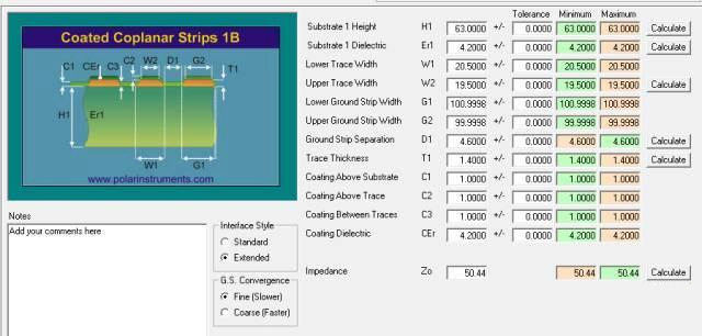
Best Practices for Matching:
- Use Controlled Impedance Traces
Define 50Ω microstrip or coplanar waveguide (CPW) structures based on your stack-up. - Design With Transmission Line Calculators
Tools like AppCAD, Saturn PCB Toolkit, or ADS LineCalc help determine trace width vs. dielectric height for the desired Z₀. - Minimize Via Transitions
Every via adds inductive discontinuity, causing impedance spikes. If unavoidable, place ground vias around signal vias for return path continuity. - Apply Matching Networks
Use LC or π networks to tune between mismatched terminations. This is essential for antennas or when interfacing with non-50Ω components.
Common Mistakes
- Using standard FR4 without accounting for dielectric changes over frequency.
- Forgetting to factor in solder mask thickness in impedance calculations.
- Overlooking discontinuities at connectors or test points.
2. Trace Geometry: Designing the Transmission Path
At RF, traces are not just wires — they are transmission lines. Their geometry defines not only impedance, but also propagation delay, phase response, and loss.
Which Geometry Should You Use?
- Microstrip: Trace on the outer layer over a solid ground plane. Good for simpler layouts but higher radiation.
- Coplanar Waveguide with Ground (CPWG): Offers better shielding, smaller return loop, and easier control over impedance.
- Stripline: Sandwiched between two ground planes. Excellent for high isolation, but harder to access and more complex stack-up.
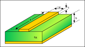
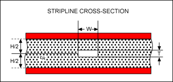
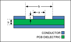
Design Guidelines
| Geometry | Controlled by | Loss Performance | EMI Behavior |
|---|---|---|---|
| Microstrip | Trace width, dielectric height | Moderate | More radiation |
| CPWG | Trace + gap + side grounds | Better | Reduced EMI |
| Stripline | Trace width + dielectric above and below | Best | Low EMI |
- Avoid abrupt trace width changes — they cause impedance steps.
- Maintain uniform trace width — changes in copper pour can cause a mismatch.
- Keep RF trace lengths as short as possible, especially between matching elements.
Simulation Tip
Use EM solvers like HFSS or Sonnet to simulate trace geometries in a real stack-up. This helps predict parasitics not captured in simple calculators.
3. Dielectric Constant (Dk): Governing Wave Propagation
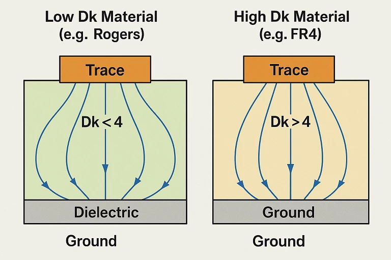
The dielectric constant of your PCB substrate directly affects signal speed, impedance, and crosstalk. High Dk reduces signal velocity, but inconsistent Dk leads to timing skew and distortion.
What Makes Dk Critical?
- Impedance is inversely related to √Dk.
- Phase delay (θ) = βL depends on Dk.
- Variation in Dk between layers causes signal skew, especially for differential pairs.
Material Considerations
| Material | Dk | Suitable For |
|---|---|---|
| FR4 | 4.2–4.8 (varies) | Low-frequency (≤1 GHz) |
| Rogers 4003C | 3.38 | RF up to 10 GHz |
| Rogers 4350B | 3.48 | High-power RF |
| Isola I-Tera MT40 | 3.45 | Broadband, low loss |
- Choose low and stable Dk across temperature and frequency.
- Dk must be uniform across the panel to ensure phase alignment in phased-array or timing-critical circuits.
Real-World Pitfall
FR4’s Dk varies ±10% across frequency and humidity. A design simulated at 2.4 GHz on FR4 might behave unpredictably on a real board, especially in outdoor or industrial environments.
4. Dissipation Factor (Df): Quantifying Signal Loss in the Material
Dissipation Factor (Df) tells you how much signal energy is absorbed by the substrate and converted to heat. High Df = greater insertion loss, which reduces signal amplitude and fidelity.
Why Df Matters at High Frequencies
- Signal loss grows linearly with frequency and trace length.
- For GHz designs, Df can impact SNR and bit error rate.
- Filters, mixers, and amplifiers may fail spec due to unexpected board loss.
Df Selection Table
| Material | Df | Recommended Frequency |
|---|---|---|
| FR4 | 0.020 | <1 GHz |
| Rogers 4350B | 0.0037 | ≤10 GHz |
| Taconic RF-35 | 0.0018 | >10 GHz |
- Use insertion loss calculators (Keysight ADS, Simbeor) to quantify impact.
- Avoid long RF traces on lossy substrates — prefer routing sensitive sections close together.
Verification Tip
Use VNA (Vector Network Analyzer) to measure insertion loss (S21) on fabricated boards and compare with your stack-up model.
5. RF PCB Material Selection: The Foundation of Performance
Material choice affects impedance, loss, thermal stability, and manufacturing yield. Choosing the wrong laminate can break your RF design before you even place components.
Key Selection Factors:
- Dk/Df Stability: Affects impedance and loss.
- CTE (Coefficient of Thermal Expansion): Must match copper and components for solder joint reliability.
- Moisture Absorption: Water ingress changes Dk and increases loss — especially critical for outdoor or medical RF devices.
- Cost vs. Performance: High-end materials are more expensive but required for >3 GHz designs.
Common Materials
| Material | Dk | Df | CTE (ppm/°C) | Notes |
|---|---|---|---|---|
| FR4 | 4.4 | 0.020 | ~70 (z-axis) | Cheap, but lossy at RF |
| Rogers 4003C | 3.38 | 0.0027 | 46 | Excellent for 2–8 GHz |
| Rogers 4350B | 3.48 | 0.0037 | 32 | Good for PAs & mixers |
| Isola Astra MT | 3.00 | 0.0017 | 40 | Very low loss, premium boards |
6. Stack-Up Configuration: Laying the Groundwork for Performance
The PCB stack-up is not just a physical arrangement — it defines impedance control, signal isolation, EMI containment, and manufacturability. A poorly planned stack-up can cause signal reflections, loss, crosstalk, and poor thermal dissipation.
Key Design Goals
- Achieve controlled impedance for RF traces (typically 50Ω or 75Ω).
- Provide dedicated return paths for high-frequency currents.
- Shield RF signals from noisy digital/clock domains.
- Minimize layer transitions (vias) to avoid added parasitics.
Recommended Stack-Up Example (4-Layer RF + Digital Mixed Board)
mathematicaCopyEditLayer 1 (Top): RF signals
Layer 2: Solid Ground Plane (GND)
Layer 3: Power Plane + Digital Signals (if needed)
Layer 4 (Bottom): Control, low-speed, or antenna routing
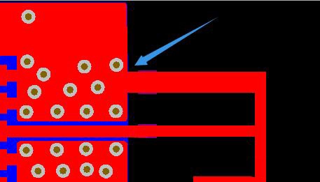
Tips:
- Place RF signals on outer layers to minimize via count.
- Put GND directly under RF layers to create tight-coupled transmission lines.
- Keep power planes separate from RF signal layers unless via stitching is carefully done.
Practical Tool
Use Polar Si8000 / Si9000 or built-in impedance calculators in Altium/Allegro to verify your stack-up meets the impedance tolerance ±10%.
Common Mistakes
- Mixing analog ground and digital ground without proper stitching.
- No solid plane under RF traces → results in current spreading and radiation.
- Skipping manufacturer DFM review — stack-up may not be fabricable as designed.
7. Grounding Strategy: Controlling Return Currents and Shielding
Grounding is arguably the most underestimated topic in RF PCB design. A bad ground design leads to EMI issues, unstable circuits, and system-wide failures — even with a perfect schematic design.
Core Principles
- Every RF signal needs a clean return path. This means there should be an unbroken GND plane directly beneath signal traces.
- Ground loop area must be minimized to reduce radiation.
- Mixed-signal systems (RF + digital) require a partitioned ground with careful join points.
Design Tips
- Use solid, continuous ground planes under all RF routing layers.
- Place via fences (ground vias every λ/20) around sensitive signal paths to contain energy.
- For critical analog/RF ICs, give each one a local ground pour connected to the main GND via multiple short vias.
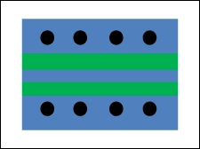
Example: Ground Stitching
luaCopyEdit|--- RF Trace ---|
|GND via|       |GND via|
|       |       |       |
|-- GND Plane (L2) -----|
- Stitch vias every 0.25″ (~6mm) or less at RF frequencies.
- Place GND vias around SMA connectors, matching networks, and filter circuits.
Watch Out For:
- Ground plane cuts or splits beneath signal traces.
- Long return current paths due to component placement on opposite layers.
- Using “via islands” instead of continuous GND — increases loop area.
8. Crosstalk Control: Managing Interference in Compact Layouts
Crosstalk is the unwanted coupling of signals between nearby traces. It worsens with higher frequency, longer parallel runs, and inadequate spacing.
How Crosstalk Happens
Two RF lines running in parallel over a shared reference plane can couple via:
- Capacitive coupling: from overlapping electric fields.
- Inductive coupling: from shared magnetic flux loops.
Design Guidelines to Reduce Crosstalk
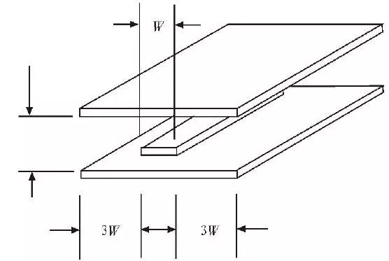
- Apply the 3W Rule: spacing between traces = 3× trace width minimum.
- Use orthogonal routing between layers (horizontal on one, vertical on the other).
- Place ground traces or stitching vias between critical signals.
- Avoid placing high-speed digital lines close to analog or RF traces.
Crosstalk Simulation
Use HyperLynx, Allegro SI, or SiSoft QSI to simulate coupling between nets pre- and post-layout.
Tip: If you can’t avoid parallel routing:
- Increase vertical separation (e.g., move one signal to another layer).
- Add guard traces tied to GND.
Real-World Symptom
Your filter behaves perfectly in simulation, but performance tanks in the prototype — likely due to crosstalk or poor isolation.
9. Component Placement: Signal Flow, Parasitics, and Isolation
The physical location of components determines your RF signal quality, parasitic loading, and fabrication success.
Placement Guidelines
- Route signals in logical signal flow order (source → match → amp → antenna).
- Keep matching networks as close as possible to the RF pins — no long stubs!
- Place bypass capacitors within 0.5 mm of power pins and tie with short GND vias.
- Separate noisy blocks (clocks, DC-DCs) from sensitive analog/RF ICs.
Zoning Principle
Group components by function:
- RF Front-End
- Power Management
- Digital Processing
- Antennas/Output Stages
Use moats or cutouts in GND planes (with stitching via fences) to separate zones while maintaining a single-point ground reference.
Real-World Suggestion
Before layout, print out a 1:1 scale floorplan on paper and do a component placement review with your hardware team — this often reveals mistakes that layout software can’t.
10. Thermal Management: Protecting Performance Under Heat
RF circuits — especially power amplifiers and transmitters — generate heat. Excess heat not only reduces efficiency but shifts electrical parameters like gain, frequency, and linearity.
Cooling Techniques
- Place thermal vias under power devices to connect the thermal pad to internal GND planes or external heat sinks.
- Use wide copper pours under heat-generating components.
- Consider embedded copper coins or thermal relief patterns for very high-power designs.
Design Targets
- Keep junction temperature (Tj) below 85°C for most RF ICs.
- Plan for <10°C/W thermal resistance from junction to board for PAs.
Simulation Tools
Use Ansys Icepak, SolidWorks Flow Simulation, or Mentor FloTHERM to model thermal distribution in pre-layout planning.
Common Mistakes
- Forgetting to connect the exposed pad to GND with enough vias.
- Using thin copper (e.g., 0.5 oz) for high-power RF paths.
- Routing RF over hotspots like DC-DC converters.
Summary: Making RF PCB Design Practical
RF PCB design is not just about theory — it’s about making practical, physics-informed layout decisions. These 10 factors aren’t isolated — they work together. For example:
- Impedance relies on trace geometry + stack-up + material.
- Crosstalk depends on spacing + grounding + placement.
- Thermal affects material choice + layout + performance.
If you apply these principles with simulation, measurement, and thoughtful design — your RF designs will not only work but work reliably.
Need help with your RF PCB design project? Contact IWDF Solution today for expert engineering support and fast quotations.

