

Equipment downtime is costly — every idle hour hits the bottom line. When engineers trace the fault back to a single circuit board that has been discontinued, has no design files, and cannot be sourced, the assumption is often that buying brand-new equipment is the only way forward. It is not. That is exactly what PCB reverse engineering is for.
PCB reverse engineering is the process of analyzing a physical circuit board to reconstruct its schematics, Bill of Materials (BOM), and design files (Gerber) for repair, cloning, or obsolete component replacement. It involves imaging, component de-soldering, and tracing connections using tools like multimeters, X-rays, and specialized software to recreate the full CAD data — without access to any original design files.
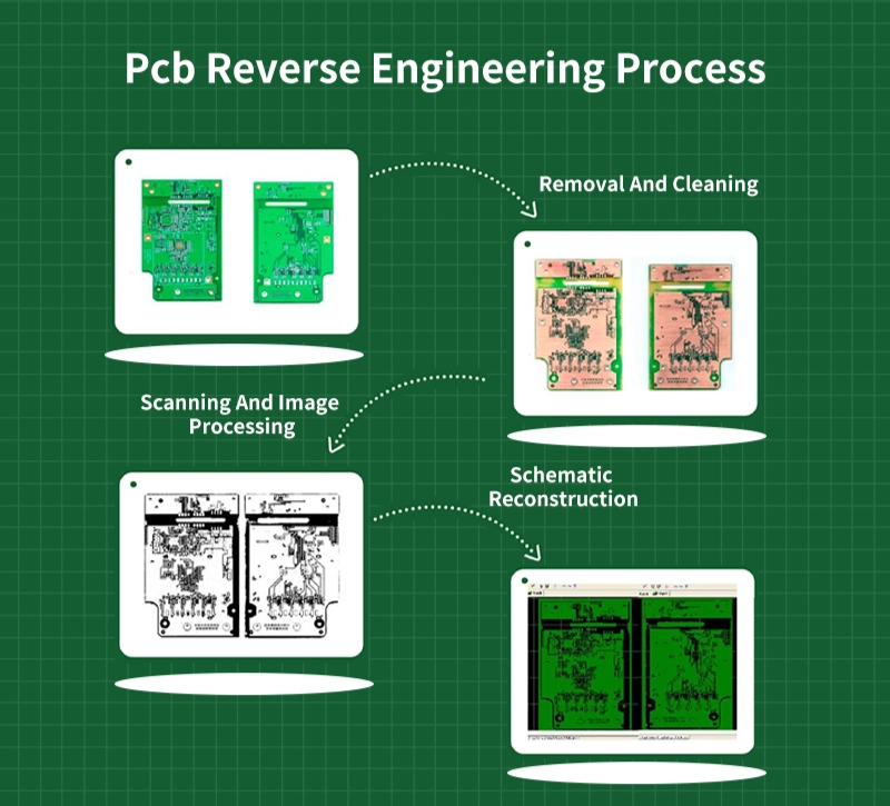
This guide covers the full process from start to finish — what PCB reverse engineering actually involves, how each step works, what tools and techniques professionals use, and what to look for when choosing a service provider. Whether you are dealing with a failed industrial board, an obsolete product that still needs to be manufactured, or design files that no longer exist, you will find a clear and practical answer here.
What Is PCB Reverse Engineering?
PCB reverse engineering is a structured, multi-stage process. It starts with a physical circuit board and ends with a complete, production-ready design package. The process uses a combination of visual inspection, X-ray imaging, component measurement, schematic reconstruction, and layout redrawing to recreate design data that either never existed in accessible form or was permanently lost.
The output — schematic diagrams, Gerber files, BOM, and stackup specification — is functionally equivalent to what an original design engineer would produce during new product development. It can be sent directly to any PCB manufacturer in the world for fabrication.
What makes PCB reverse engineering technically challenging is not any single step. It is the precision required across all of them. One misidentified component can create a net error that only becomes visible when a prototype fails. Professional service providers manage this through systematic documentation and cross-verification at every stage — which is why the process described below follows a strict sequence.

PCB Reverse Engineering vs. PCB Cloning — What Is the Difference?
These two terms are often used interchangeably, but they are not the same service.
| PCB Reverse Engineering | PCB Cloning | |
|---|---|---|
| Goal | Understand and optionally improve the design | Replicate the board exactly as-is |
| Output | Schematic + Gerber files + BOM + optional redesign | Gerber files for direct manufacturing |
| Improvements possible? | Yes — engineers can upgrade components or fix flaws | No — design flaws are copied too |
| Best for | R&D, legacy repair, compliance redesign, lost files | Fast replacement, mass production of an existing board |
| Technical complexity | Higher | Lower |
At IWDF Solutions, most clients need reverse engineering first — and then cloning for production. The two services work together.
What Are the Real Benefits of PCB Reverse Engineering?
PCB reverse engineering gives you control over hardware you depend on — even when the original designer, manufacturer, or documentation no longer exists. It converts a physical board into a documented, manufacturable, and modifiable design asset.
Six Practical Benefits Worth Knowing
1. Avoid the cost of replacing entire machines
When a single PCB fails in a production environment, replacing the whole machine is often the only option — unless you can reproduce the board. Reverse engineering that one board can bring an entire production line back online at a cost that is a fraction of buying new equipment. For product engineering teams, this is not just a technical decision. It is a financial one.
2. Recover from lost or incomplete design files
Company acquisitions, staff turnover, server crashes, and poor documentation practices all lead to the same outcome: hardware exists but the design data is gone. Reverse engineering recovers the full design package from the physical board — schematic, BOM, Gerber files, and stackup specification.
3. Replace obsolete or end-of-life components
A microcontroller used in a 2010 design is no longer available. A MOSFET driver has been discontinued. Reverse engineering allows engineers to understand the existing circuit and substitute verified modern equivalents — without rebuilding the design from scratch. This extends the serviceable life of a product by years.
4. Accelerate new product development
A new product that would normally take 2–3 years to develop from scratch can sometimes reach prototype stage in months when an existing design is used as the starting point. Reverse engineering extracts that starting point from the physical hardware.
5. Detect counterfeit or tampered components
Defense, aerospace, and medical device supply chains use reverse engineering to verify that boards received from suppliers match their specifications. Unauthorized component substitutions and embedded malicious circuits can be identified through systematic analysis.
6. Enable redesign and performance upgrades
Unlike cloning — which copies a board exactly, flaws and all — reverse engineering gives you a fully editable design. That means you can add wireless connectivity to a legacy controller, upgrade to a lower-power processor, or redesign for RoHS compliance without starting from zero.

When Should You Reverse Engineer a PCB?
Not every hardware problem requires PCB or PCBA reverse engineering, and in some cases, buying a replacement product is cheaper and safer. However, there are several common situations where reverse engineering becomes the only realistic path forward.
- Legacy equipment with no documentation
Many factories still run critical machines built 10–20 years ago, where the original supplier is gone and no design files exist, leaving only the populated PCB. - Obsolete or discontinued components
Key ICs, power modules, or connectors may be end‑of‑life, forcing you to redesign the board or qualify replacements without original schematics. - Need for a second source or new manufacturing partner
If your existing PCB supplier is unreliable or too expensive, you may need complete design data to move production to a different factory. - Cost reduction, redesign, or feature extensions
Reverse engineering can be the first step toward optimizing the layout, improving EMC, or integrating new communication interfaces while preserving core functionality. - Failure analysis and repair
Having a schematic derived from an existing board makes it much easier to diagnose faults, isolate weak points, and implement more robust repairs.
Reverse engineering is a tool, not a goal; the real aim is to regain control over your hardware lifecycle, whether that means continued maintenance, redesign, or migration to a new PCB and PCBA partner.


How to Reverse Engineer a PCB: The Full Step-by-Step Process
The 10 steps below reflect the industry-standard workflow used by professional PCB reverse engineering services worldwide. The order is not arbitrary — each step creates the foundation that the next one requires.
Step 1 – Define Your Goal and Scope
Before you handle the board, decide exactly why you are reverse engineering it and what success looks like.
- Clarify the end goal
- Maintenance only: You just need to reproduce the same board so you can keep the equipment running.
- Redesign: You want to update components, improve reliability, or shrink the board.
- Understanding: You mainly want to understand how a circuit works (for debugging, integration, or training).
- Decide what must stay the same
- Mechanical: Board outline, mounting holes, connector positions and pinouts, front‑panel alignment.
- Electrical: Supply voltages, input/output ranges, timing, communication protocols, safety distances.
- Decide what can change
- Component brands and packages (for example, SOT‑223 regulator replaced by a more modern SMD).
- Layout details, as long as EMC, safety, and performance remain within your requirements.
Write this down as a short requirements document. Treat the reverse‑engineered board like any normal new design project: it has a specification, a budget, and a deadline.
Step 2 – Clean, Inspect, and Document the PCB
Think of this as creating a “digital twin” of the original board.
- Stabilize and clean
- Disconnect the PCB from all cables and power sources.
- If the system works at high voltage (for example, mains AC, large motor drives), wait for capacitors to discharge or manually discharge them with proper safety procedures.
- Use isopropyl alcohol (IPA) and a soft ESD‑safe brush to remove dust and flux; avoid soaking stickers or labels that may contain part numbers or revision info.
- Inspect physically
- Look for damage: burnt areas, lifted pads, cracked components. Take photos of any anomalies.
- Check the board edge with a loupe: count visible copper bands to estimate how many layers there are. If you see only two but routing is extremely dense, assume internal layers exist.
- Measure and note mechanical data
- Use calipers to measure board length, width, thickness, and distance between mounting holes.
- Sketch a quick mechanical drawing (even on paper) with dimensions and hole locations. This will help when recreating the outline in CAD later.
- Photograph systematically
- Place the board on a flat, neutral‑colored background.
- Take perpendicular high‑resolution photos of the top and bottom; try to avoid perspective distortion.
- Include a ruler or caliper in at least one image for scale.
- Take close‑ups of: dense areas (MCUs, BGAs, RF modules), power sections, and connectors.
- Save the images with clear names (for example, board_top_overview.jpg, board_bot_corner1.jpg).
- Organize documentation
- Create a project folder and subfolders such as: /photos, /processed_images, /notes, /bom.
- Start a text file or spreadsheet for general notes (board label, version, location in equipment, symptoms if it is failing).
This preparation step makes the rest of the work much easier and more reliable.
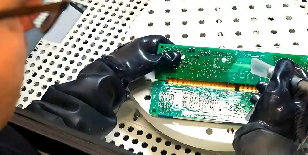
Step 3 – Identify and Label Components
Now you convert the physical parts on the PCB into structured data.
- Build a component map
- Open your top and bottom photos in an image editor.
- On each side, add a transparent layer and draw a small box or mark on every component.
- Label each component with a reference designator. If the original silkscreen is clear, copy it (R101, C5, U3). If not, create your own consistent system (for example, start ICs at U100, resistors at R100).
- Read markings and collect datasheets
- For ICs and small packages, use a microscope or a USB camera to read their markings.
- Search for the marking plus package type (for example, “STM32F103 LQFP64”) to find datasheets.
- Save datasheets in a /datasheets folder and name them clearly.
- Classify passives and simple parts
- For resistors with readable codes, note the value (for example, 102 = 1 kΩ).
- For capacitors and inductors, there may be no obvious markings; you may need to desolder and measure a few critical parts later (for example, timing capacitors around crystals, current‑sense resistors).
- Identify diodes, LEDs, fuses, and jumpers; note polarity and orientation based on the silkscreen and pad shapes.
- Start your BOM spreadsheet
Include at least these columns:- RefDes (R101, C5, U3…)
- Category (resistor, capacitor, MCU, connector…)
- Description (for example, “32‑bit MCU, 72 MHz, 64 pins”)
- Manufacturer and part number (if known)
- Value / rating (for example, 10 kΩ, 1%, 50 V)
- Package (0805, TQFP64, SOIC‑8…)
- Notes (for example, “may be obsolete”, “custom marking”, “measure later”).
- Deal with unknown or “sanded” parts
- If an IC has no readable marking, look at what it connects to: power pins, crystals, communication lines (UART, CAN, SPI, Ethernet).
- Compare its pinout and package with common MCUs, FPGAs, or driver chips to narrow down the likely type.
- In some projects, you do not need a perfect 1:1 match: if you can understand its function and interface, you can redesign that block using a modern or documented component.
By the end of this step, you should have a reasonably complete, structured view of the bill of materials.
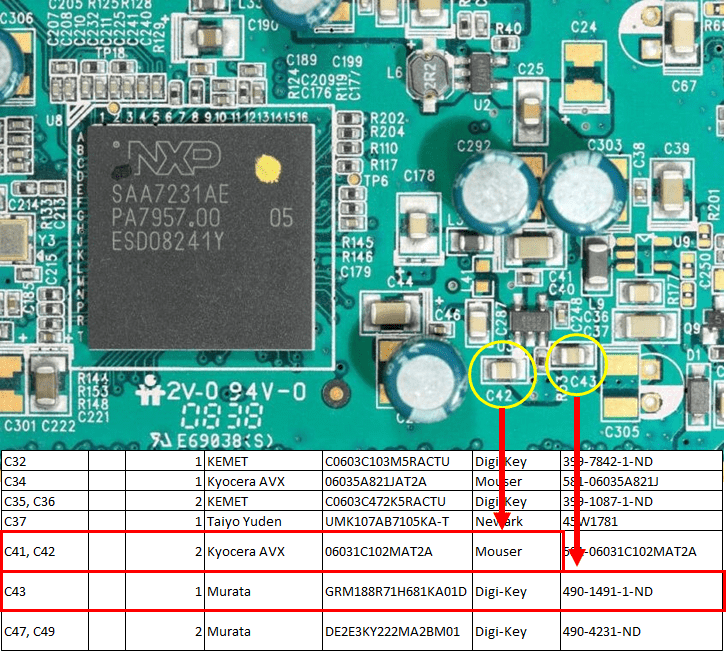
Step 4 – Capture Copper Traces and Layer Structures
This step transforms pictures of copper into a map of where signals travel.
- Prepare images for tracing
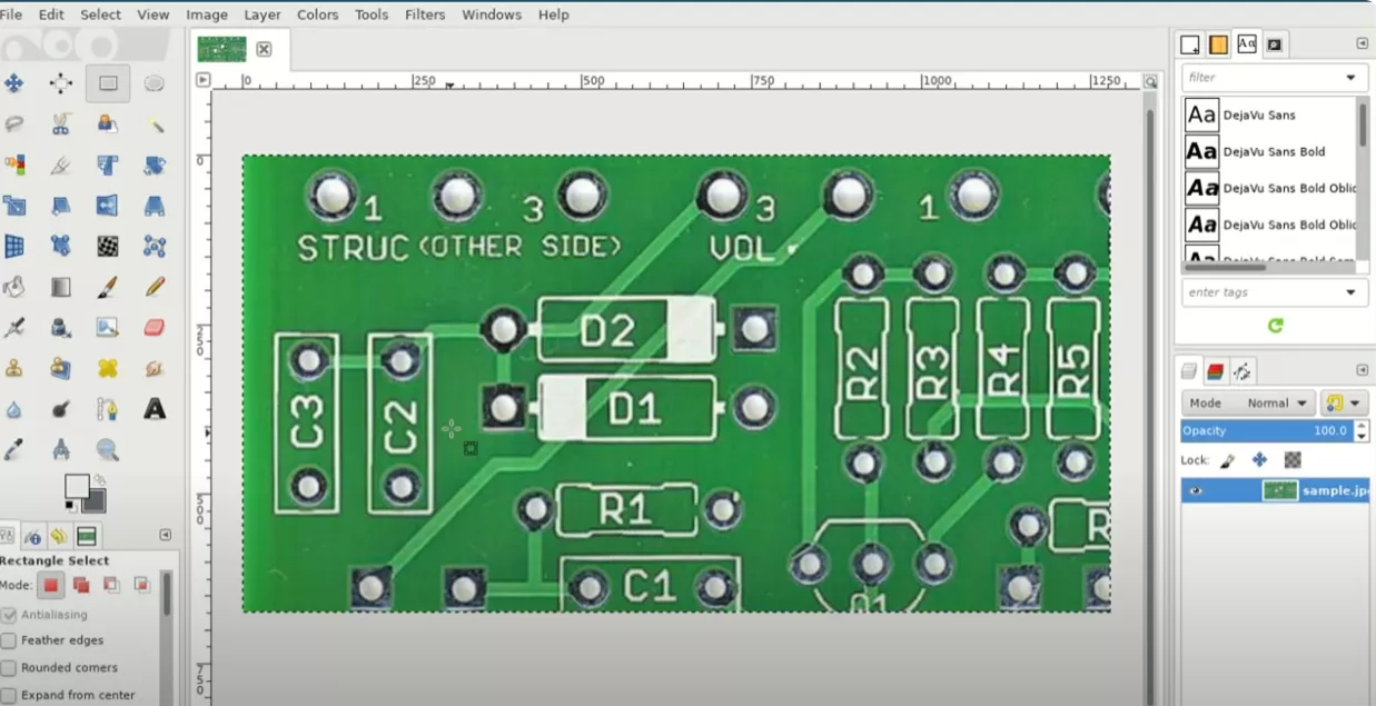
- Take your top and bottom overview photos and convert them to grayscale in an editor.
- Increase contrast and tweak brightness so copper tracks stand out clearly from the solder mask.
- Create an overlay layer where you “paint” all pads and vias with a solid color, matching their size. This makes it easier to see where connections start and end.
- Align top and bottom
- Create a large canvas and place the top and bottom images on separate layers.
- Rotate, scale, and move them until through‑holes, fiducial marks, and board outlines line up.
- Use at least three known points (for example, three mounting holes) to verify alignment in different areas.
- Trace major nets first
- Start with ground and main supply rails; they usually have large copper pours or wide traces.
- Color these nets in your overlay (for example, all ground areas in blue, main supply in red), so you can easily recognize them later.
- Identify decoupling capacitor connections between power pins and ground: they help you confirm which net is which.
- Trace signal connections
- Choose one IC or connector and follow each pad outwards, marking the trace in a unique color per net or per group of related nets.
- When a trace disappears under a component, check the other side of the board for a via at the same position; if present, your trace likely continues there.
- Take notes when a trace appears to dive into an internal layer via a via that has no visible continuation on top or bottom.
- Handling multilayer boards
- For boards with inner layers, visible traces will not tell the full story. Mark every via that seems to connect to inner routing only.
- If the project justifies the effort and cost, plan for additional techniques:
- X‑ray imaging to see inner-layer connections and BGA pads.
- Professional delayering: remove components, then sand or mill the board layer by layer, photographing each copper layer before going deeper.
- Maintain a net log
- As you identify a net (for example, “MCU reset line from U1 pin 7 to connector J3 pin 2”), write it down in a log or directly into your schematic notes.
- Use stable net names (RESET, CAN_H, CAN_L, etc.) so you can track them consistently across images, notes, and CAD.
This step is time‑consuming, but it is the foundation of your schematic and layout recreation.
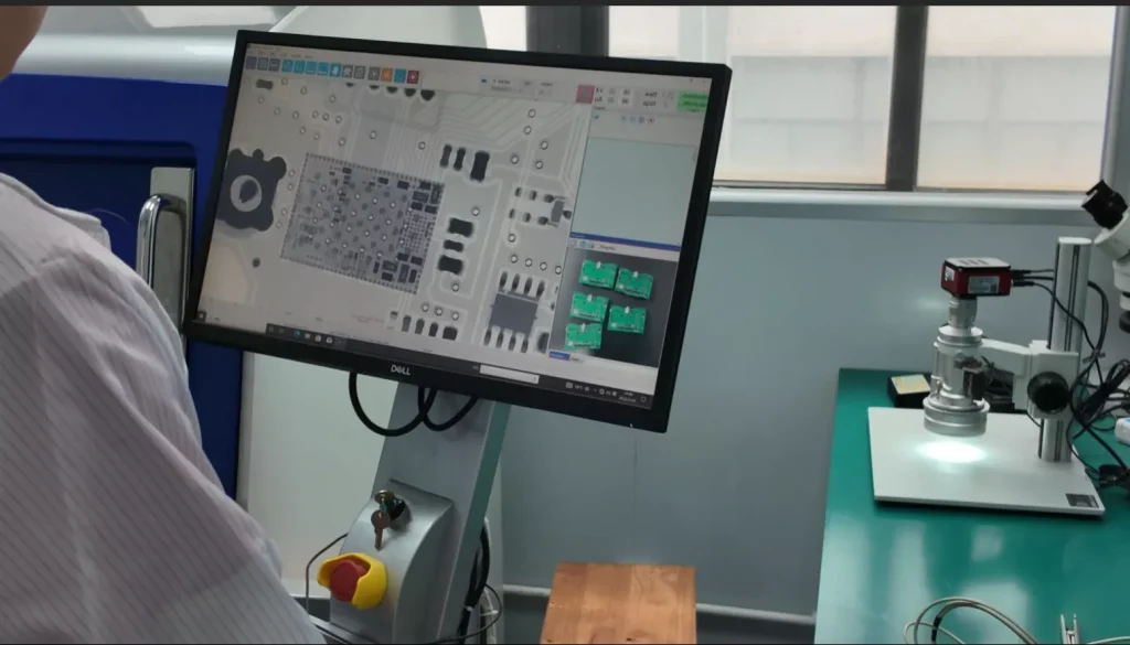
Step 5 – Map Nets and Create a Provisional Schematic
Now you create the logical circuit from all the physical connections you have observed.
- Start with power and ground blocks
- For each power rail you identified, draw a small power distribution section in your schematic.
- Place the connectors or input terminals, fuses, surge suppression parts, rectifiers, and regulators in a logical flow: input → protection → conversion → filtering → loads.
- Label each output net (for example, +24V, +12V, +5V, 3V3, VREF) and connect decoupling capacitors according to what you saw on the board.
- Build functional modules
- Group the rest of the schematic by function:
- Microcontroller or CPU core (clock, reset, programming/debug pins).
- Communication interfaces (RS‑485, CAN, Ethernet, USB, etc.).
- Sensor inputs or analog front‑ends.
- Power drivers (motors, relays, MOSFETs, IGBTs).
- For each block, place the main IC and surrounding discrete components, and wire them according to your traced nets.
- Group the rest of the schematic by function:
- Use datasheets as a roadmap
- Keep each component’s datasheet open and compare typical application circuits with what you see.
- For example, voltage regulators often follow a standard application circuit; if your board matches it, you can cross‑check component values and net connections.
- This also helps you guess missing values when markings are unclear.
- Systematically add nets
- For each connection you traced (for example, MCU pin PA9 goes to RS‑485 driver A input), assign a clear net name and draw it in the schematic.
- Avoid long “spaghetti” wires; use net labels to keep the drawing readable, especially when nets jump between pages.
- Iterate and validate
- After finishing a block, print it or view it on a tablet and sit with the physical board in front of you, checking each connection.
- Use a continuity tester to confirm ambiguous paths.
- Mark uncertain areas in your schematic with comments, so you remember to revisit them later during testing.
By the end of this step, you should have a schematic that describes how the board works, even if a few details still need confirmation.
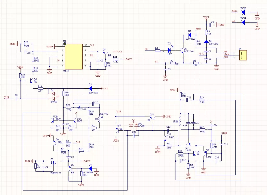
Step 6 – Reconstruct the PCB Layout
Here, you recreate the physical board in your PCB CAD tool, guided by your photos and schematics.
- Set up the project and board outline
- Create a new PCB project and import your schematic.
- In the layout editor, draw the board outline using the dimensions you measured earlier.
- Add mounting holes, slots, and mechanical keep‑out areas to match the original.
- Use board photos as references
- Many CAD tools allow you to place bitmap images on a mechanical layer.
- Place the top photo as a background, scale and align it so mounting holes and connectors line up with your drawn outline.
- Do the same for the bottom side in another view or layer.
- Place components according to the original board
- Start with connectors: they must line up with external cables, front panels, or backplanes.
- Place large components (transformers, large capacitors, relays, heatsinks) next, matching positions on the photo.
- Then place ICs, small passives, and other parts, respecting orientation and small alignment details when they matter (for example, symmetrical pairs in differential circuits).
- Recreate routing priorities
- Identify critical nets: clocks, high‑speed buses, differential pairs, precision analog paths, or high‑current traces.
- Route these first, following the original path and reference planes as closely as practical.
- Then route remaining signals in an orderly fashion, keeping similar grouping to the original when it helps.
- Apply realistic design rules
- Set trace width/clearance rules according to both what you see on the original and what your manufacturing partner can actually produce.
- For high‑voltage or safety‑critical areas, apply wider creepage and clearance distances in line with standards and the original design.
- Check against photos
- Regularly compare the in‑progress layout with your overlay images to see whether component positions, trace paths, and via patterns match your expectations.
- Small differences are acceptable for non‑critical signals, but large deviations in power or high‑speed sections may cause performance or EMC problems.
The aim is a layout that behaves like the original board and can be manufactured reliably, not a pixel‑perfect copy of every track.

Step 7 – Build a Complete, Production‑Ready BOM
Now you refine your preliminary BOM into something that purchasing and manufacturing can actually use.
- Consolidate part data
- Merge your earlier spreadsheet with the references from your schematic.
- Check that every component on the schematic appears in the BOM with a defined value and package.
- Add manufacturer and distributor details
- For each part, add the preferred manufacturer and their part number.
- For common passives, you can specify generic series and allow substitutions within certain tolerances.
- For critical ICs, choose exact part numbers and list acceptable alternates if compatible.
- Evaluate obsolescence and risk
- Use distributors’ websites and manufacturer information to check lifecycle status (active, NRND, EOL).
- For parts that are hard to source or near end‑of‑life, plan replacements or redesigns now instead of waiting for a future shortage.
- Include assembly information
- Add fields such as “Placement Side” (top/bottom), “DNP” (do not populate) for optional components, and any special handling notes (for example, “program after assembly”, “ESD sensitive”).
- This helps your manufacturing partner set up production faster and reduces manual clarification later.
The BOM is where your reverse engineered design connects with the real supply chain, so treat it with the same care as the schematic and layout.

Step 8 – Check Manufacturability and Reliability (DFM/DFR)
Before ordering boards, you want to catch obvious manufacturability and reliability problems.
- Run automated checks
- Use your CAD tool’s design rule check (DRC) for clearances, minimum trace widths, drill sizes, and unconnected nets.
- If available, use a DFM plugin or your manufacturer’s rule set to catch issues like slivers, acid traps, or insufficient solder mask dams.
- Perform manual sanity checks
- Inspect high‑current paths and confirm that traces and copper pours are wide enough and thick enough to handle the expected current and thermal load.
- Check high‑voltage areas for adequate creepage and clearance distances, including across the PCB surface and through air.
- Make sure test points or accessible pads exist for key signals (power rails, communication lines), especially if you will need to debug boards during bring‑up.
- Consider the environment and standards
- Think about operating temperature range, humidity, vibration, and any regulatory standards the final product must meet (for example, medical, industrial safety).
- If needed, revise component choices, pad sizes, or mechanical supports (for example, glue, brackets) to meet these conditions.
Addressing these points early helps prevent expensive rework after you have already built prototypes.
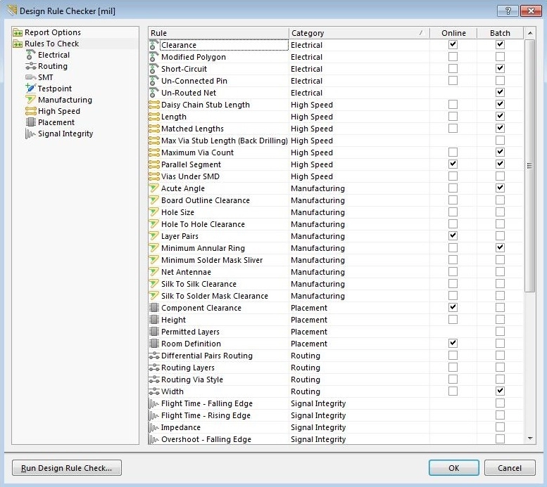
Step 9 – Prototype, Test, and Iterate
This is where you prove that your reverse engineered design actually works.
- Order and inspect prototype PCBs
- Place a small order (for example, 3–10 boards) using the same stack‑up, copper thickness, and surface finish you expect for production.
- When boards arrive, visually inspect them: check for shorts in fine‑pitch areas, correct drill positions, and board dimensions.
- Assemble prototypes
- For very low quantities, you can assemble by hand, but for complex boards it is better to use a professional assembly line.
- Ensure that the assembly team has the latest BOM, placement files, and clear orientation markings for polarized components.
- Bring‑up procedure
- Power up the board through a current‑limited supply and gradually increase voltage while monitoring current draw and temperature.
- Verify that each power rail is present and correct using a multimeter or oscilloscope before enabling the rest of the system.
- Connect to communication interfaces and check basic functionality (for example, microcontroller programming, serial communication, status LEDs).
- Compare against original behavior
- If you still have working original boards, run them side by side with the new boards under the same conditions.
- Measure key signals (for example, clock frequencies, bus waveforms, analog values) and compare their shape, amplitude, and timing.
- Note any differences and decide whether they are acceptable or indicate a real design or reverse engineering error.
- Iterate as needed
- Update your schematic, layout, and BOM based on the issues you find (for example, wrong pin mapping, missing pull‑up resistor, incorrect component value).
- If changes are significant, run another small prototype round before committing to volume.
Iterating is normal; even original designs rarely go from first layout to mass production without changes.
Step 10 – Document and “Productize” the Reverse Engineered Design
The final step is to turn the project into a maintainable part of your product portfolio.
- Organize all design files
- Store schematics, layout files, Gerbers, drill files, stack‑up information, BOM, and assembly files in a version‑controlled repository.
- Tag the revision that matches your validated prototype as a baseline (for example, “Reverse‑eng board rev A, validated”).
- Capture test and validation procedures
- Write down the bring‑up steps, test cases, and acceptance criteria you used to validate the board.
- Include any special test jigs, software tools, or measurement setups required.
- Record design decisions and limitations
- Note where you deviated from the original design and why (for example, “Updated regulator IC for availability”, “Improved creepage in power section”).
- Document any assumptions you had to make during PCB reverse engineering and how they were validated.
- Prepare for hand‑off to manufacturing or external partners
- Package the necessary documentation for your internal factory or external suppliers so they can build the board without constant questions.
- Define who owns and maintains the design internally, so changes are controlled.

What Tools Do Professionals Use for PCB Reverse Engineering?
Depending on board complexity, you’ll need a combination of the following tools and software. We’ve organized them by category to help you prioritize your use.
Hardware Tools and Equipment
Imaging and Documentation Tools
- Flatbed scanner (600+ DPI recommended) for consistent, distortion-free board imaging
- High-resolution digital camera (12MP minimum) with tripod or fixed mount for consistent orthogonal photography
- Digital microscope (40×–200× magnification) for inspecting fine traces, solder joints, and component markings
- Lighting setup with adjustable angle and intensity to minimize reflection and enhance copper/trace visibility
Cleaning and Preparation
- Isopropyl alcohol (99%) for removing flux, corrosion, and conformal coatings
- Soft brushes and lint-free cloths to avoid scratching pads or traces
- Acetone (optional) for removing stubborn conformal coatings without damaging components
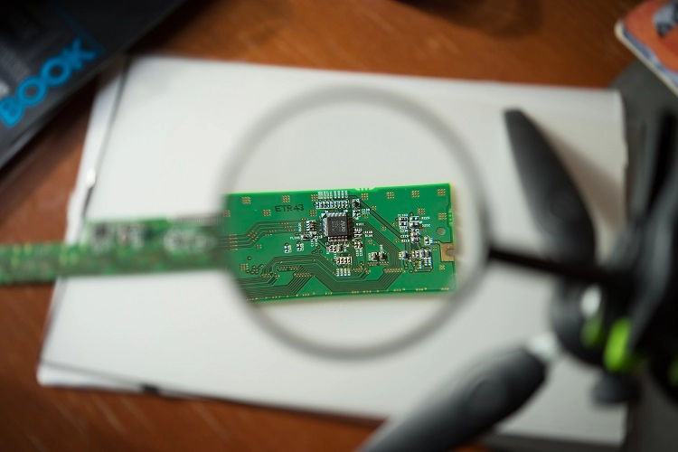

Measurement and Testing Equipment
- Digital multimeter with continuity/resistance/diode testing modes for tracing connections
- Calipers or a micrometer for precise component footprint measurements
- Logic analyzer (optional, for signal-level analysis on complex boards)
- Oscilloscope (optional, for validating analog circuit behavior during testing)
Delamination Tools (for Multilayer Boards)
- Fine-grit sandpaper (800–2000 grit) for gradual, controlled layer removal
- CNC milling machine or surface grinder (professional-grade) for precision delayering
- Chemical etching solutions (controlled PCB etchant) for layer-specific removal
- X-ray equipment (professional facility access) for non-destructive multilayer imaging
Image Processing and Tracing Software
Free/Open-Source Options
- GIMP – comprehensive image editing; layer management and alignment tools for stacking multiple board images
- Inkscape – vector graphics editor ideal for manual trace mapping and creating clean line drawings
- Photoshop (alternative) – if budget permits; superior layer blending and alignment features
Specialized PCB Image Tools
- KiCad bitmap2component – automated conversion of scanned PCB images into vector outlines
- ImageMagick – a command-line tool for batch image processing, alignment, and scale correction
EDA (Electronic Design Automation) Software
Professional-grade software for schematic and PCB layout recreation:
| Software | Cost | Best For | Ease of Use |
|---|---|---|---|
| KiCad | Free | Students, hobbyists, and professionals; strong community | Good—intuitive UI |
| Eagle CAD | $69/year (Personal) | Beginners to intermediate; smaller boards | Moderate—steeper learning curve |
| Altium Designer | $3,000+/year | Professional engineers; complex multilayer boards | Moderate—powerful but expensive |
| Proteus/Labcenter | $500–$2,000 | Educational; mixed schematic + simulation | Moderate—older interface |
| OrCAD/Cadence | Custom licensing | Enterprise; mixed-signal designs | Moderate—extensive toolset |
[NEW RECOMMENDATION] For most reverse engineering projects, KiCad is the optimal choice: it’s free, professionally capable, has excellent documentation, and benefits from continuous community development. If you require advanced simulation, Altium Designer is the industry standard in professional services.
Optional/Advanced Tools
Design Rule Check (DRC) software – Validates your recreated design against manufacturing constraints
Automated trace extraction software – Some providers use proprietary AI/ML tools to detect traces automatically and via connections from scanned images
Netlist extraction tools – Automated conversion of physical connections into electrical netlists
What Should a PCB Reverse Engineering Service Deliver?
When you hire a professional service, you should know exactly what you are paying for. A serious provider delivers a complete, production-ready design package — not just a PDF schematic and a rough component list.
| Deliverable | Format | What It Is For |
|---|---|---|
| Schematic diagram | PDF + native EDA file (Altium / KiCad) | Circuit understanding, modification, future redesign |
| PCB layout files | Gerber RS-274X + Excellon drill | Direct PCB fabrication at any factory worldwide |
| Bill of Materials (BOM) | Excel / CSV | Component sourcing, procurement, cost estimation |
| Pick and place file | CSV / XLS | SMT assembly machine programming |
| Layer stackup specification | Material selection, impedance control, fabrication notes | |
| 3D board model | STEP file | Mechanical enclosure integration |
| Functional prototype | Assembled physical PCB | Validated proof that the reconstruction is accurate |
| Test report | Documented pass/fail results vs. the original board |
If a provider cannot deliver all of the above, ask specifically what is missing. Incomplete deliverables mean you will need to pay someone else to finish the job.
How Long Does PCB Reverse Engineering Take?
Turnaround time depends on board complexity, layer count, component density, and whether prototype validation is included. Here are realistic benchmarks based on typical project data.
| Board Type | Layer Count | Typical Turnaround |
|---|---|---|
| Simple control board | 2-layer | 5–7 business days |
| Mid-complexity board | 4-layer | 10–15 business days |
| Complex industrial board | 6–8 layer | 15–25 business days |
| High-complexity / BGA-heavy | 10–16 layer | 25–40 business days |
Rush services are available for production downtime situations. Contact us with your board details and we will confirm a precise timeline. For an accurate cost estimate, send us photos of your board and we will return a detailed quote within 24 hours — at no charge.
Why Work with a PCB Reverse Engineering Service in China?
Shenzhen is the world’s electronics manufacturing hub — and that advantage matters for reverse engineering just as much as it does for production.
Shenzhen-based engineers work within walking distance of the world’s largest component market (Huaqiangbei), the highest concentration of PCB fabrication facilities on earth, and a supply chain network that can source almost any component — including parts discontinued 10–15 years ago — faster than anywhere else.
What IWDF Solutions Offers
- Full PCB reverse engineering service — Schematic, Gerber, BOM for 1–16 layer boards
- PCB cloning — Exact board duplication for legacy replacement and mass production
- PCB design from scratch — New product design using Altium Designer, meeting IPC-2221 standards
- PCB fabrication — From single prototypes to high-volume production runs
- Turnkey PCBA assembly — SMT, THT, BGA, QFN, full component sourcing included
- Functional testing — ICT, flying probe, AOI, X-ray, burn-in testing
Everything happens under one roof. You do not need to coordinate between a reverse engineering firm, a PCB fab, and an assembly house. One project manager handles your entire journey from a physical board sample to a validated, production-ready PCBA. Our engineering team has 10+ years of PCB reverse engineering experience. We work under NDA on every project. Our English-speaking project managers are responsive across US and EU time zones. Pricing runs significantly lower than equivalent services in North America or Europe — with no reduction in technical quality or deliverable completeness.
Frequently Asked Questions About PCB Reverse Engineering
Q1: Can you reverse engineer a PCB from photos alone?
For simple 1–2 layer boards where all components are clearly visible, photos can provide enough information to begin. But for any production-quality output, we always require the physical board. Component values on unmarked SMD passives cannot be read from a photo. Via locations on inner layers are not visible at all. Sending the physical board is the only way to ensure accurate results.
Q2: What if some of my components are obsolete or discontinued?
This is one of the most common reasons clients come to us. During BOM creation, our engineers identify all obsolete parts and find verified modern equivalents. We have direct access to Shenzhen’s component markets and authorized distributor networks, which means we can source alternatives even for parts discontinued 10–15 years ago.
Q3: Will my original board be damaged during the process?
For 1–2 layer boards and most 4-layer boards, we use non-destructive methods — high-resolution scanning and X-ray — and return your original board intact. For complex multilayer boards that require delayering, we discuss this with you before starting and always recommend sending multiple samples when available.
Q4: Can you reverse engineer a board and then manufacture it for us?
Yes — this is exactly our one-stop service model. We reverse engineer the board, validate the design with a prototype, and then move directly into PCB fabrication and PCBA assembly for your production order. Many clients place their first production order within days of receiving the validated prototype.
Q5: How do I know the reconstructed schematic is accurate?
Accuracy is confirmed through prototype validation in Step 6. A board built from the reconstructed files is assembled and tested against the known behavior of the original. If any function does not match, we trace the error back to its source and correct it before delivering final files. You receive a validated, tested result — not just an untested document package.
Q6: What information do I need to get a quote?
Send us high-resolution photos of both sides of your board, the approximate board dimensions, the layer count if you know it, the quantity you need manufactured, and your target delivery date. We will respond with a detailed quote within 24 hours.
Q7: What is the difference between PCB reverse engineering and PCB cloning?
Reverse engineering recovers the full design package — schematic, Gerber files, BOM — and gives you the option to make improvements before manufacturing. Cloning focuses on reproducing the board exactly as-is, faster and at lower cost, but without editing capability. If you want to understand or upgrade the design, choose reverse engineering. If you need an exact replacement quickly, cloning may be the better fit.
Conclusion
PCB reverse engineering is not a workaround. For companies dealing with failed legacy equipment, lost documentation, obsolete components, or the need to accelerate hardware development, it is often the most direct and cost-effective solution available.
The process is structured, logical, and repeatable when handled by an experienced team. It starts with documentation and ends with a validated, production-ready design package. Every step builds on the one before it — and skipping any step creates errors that are difficult and expensive to fix later.
At IWDF Solutions in Shenzhen, we provide complete PCB reverse engineering services: from initial board assessment through schematic reconstruction, Gerber generation, prototype fabrication, and full-volume PCBA production. One team. One roof. Full documentation. Validated results.
If you have a board that needs to be reverse engineered, send us photos and we will return a free assessment and detailed quote within 12 hours.
IWDF Solutions — PCB Design | PCB Reverse Engineering | PCB Cloning | PCBA Production | Shenzhen, China

