

Staring at a PCB with no schematic? Whether you’re repairing legacy hardware, validating supplier quality, or replicating a discontinued board, this guide shows you exactly how to reverse engineer the circuit—step by step, with tools, insight, and real techniques that save time and prevent costly errors.
To reverse engineer a schematic from a circuit board, first capture high-resolution images of both sides of the PCB. Carefully identify all components, trace their connections either visually or with continuity testing, and document the net structure. Then, use schematic capture software like KiCAD or Altium Designer to rebuild the circuit diagram. The process demands precision, patience, and the right combination of tools and techniques.
Let’s walk through the essential steps, tools, and insights you need to successfully turn a bare PCB into a clear schematic—regardless of its complexity.
What is PCB Reverse Engineering?
PCB reverse engineering is the process of analyzing a printed circuit board to identify its components and interconnections, ultimately recreating a schematic or netlist. It is commonly used for repairing legacy hardware, recovering lost design data, or competitive analysis.


Quick Guide: 7 Steps to Reverse Engineer a Schematic From a PCB
While there’s no shortcut to reverse engineering, some approaches can make the process more manageable, especially for simple or two-layer boards.
- Capture High-Res Images: Photograph both sides using a macro lens or flatbed scanner.
- Desolder Components (Optional): Remove parts for clearer visibility of traces if necessary.
- Process Images: Align top and bottom layers using software like GIMP or Photoshop.
- Identify Components: Log all parts (BOM), including values and package types.
- Trace Connections: Map the nets (copper paths) using a multimeter or continuity tester.
- Draft Schematic: Rebuild the circuit in CAD tools like KiCad or Altium Designer.
- Verify & Test: Run ERC (Electrical Rule Check) and compare against the physical board.
Step 1: Prepare the tools and software you need for PCB reverse engineering.
Before touching the PCB, you must gather the right tools. Working without the proper equipment often leads to missed traces, wrong connections, or damaged boards. The required tools fall into three categories:
1.1 Essential Physical Tools
- High-resolution digital camera (preferably DSLR or mirrorless) with macro lens — to capture fine details of component markings and trace routing.
- Good lighting setup — LED light panels or ring lights to eliminate shadows and reflections.
- Magnification tools — Stereo microscope or digital microscope for reading tiny component codes.
- Multimeter with continuity mode — to check connections between pins and confirm trace paths.
- Fine-tip probes — for precision when probing small SMD pads.
- PCB holder or vice — to keep the board stable during photography and testing.
- ESD protection — anti-static wrist strap and mat to avoid damaging sensitive ICs.

1.2 Optional Advanced Tools
- X-ray inspection system — critical for multilayer boards or hidden BGA pads.
- Layer-peeling system — for destructive analysis, where you scrape away layers.
- Thermal camera — to observe heat patterns if testing a powered board before teardown.
1.3 Software Tools
- CAD software for schematic capture: KiCad (free, open-source), Altium Designer (professional), OrCAD, or Eagle.
- Image editing software: GIMP (free) or Adobe Photoshop to clean and align PCB images.
- PCB to schematic converter online tools — while often unreliable for complex boards, they can help speed up repetitive work.
- Spreadsheet software — to log and label components with reference designators.

Step 2: Document and photograph a PCB for schematic reconstruction
Proper documentation is the foundation of accurate reverse engineering. Skipping this step will cost you hours later.
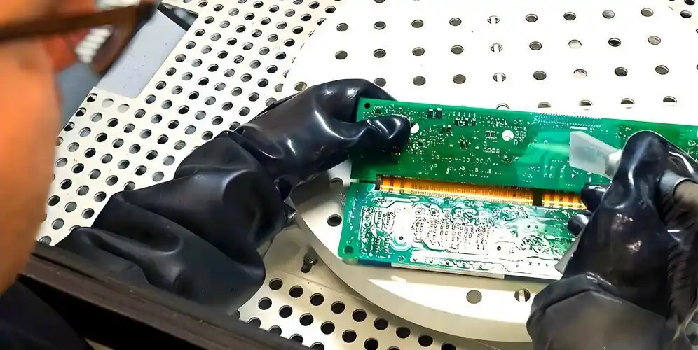
Cleaning the PCB
- Use isopropyl alcohol (IPA) and a lint-free cloth to remove dust, dirt, and solder flux residue.
- This ensures markings on components and silkscreen labels are visible in photos.
Setting up photography
- Mount the PCB on a flat, stable surface under even lighting.
- Position the camera directly above the board to avoid perspective distortion.
- Take multiple overlapping high-resolution photos of each side (front and back).
- If possible, photograph the board without components (after careful desoldering) for better trace visibility — but only if the board can be reassembled or is already non-functional.
Photo processing
- Use an image editor to stitch overlapping images into one large, high-resolution reference.
- Adjust contrast and sharpness to make copper traces stand out.
- Save versions of the image with different layers marked:
- One for component placement
- One for traces and vias
Step 3: Identify and label components on the board
This stage is where you start converting a photographed board into usable data. Accuracy here will save hours when building the schematic.
Assigning Reference Designators
- Use the manufacturer’s silkscreen markings whenever possible (e.g., R1, C2, U5).
- If the board has no silkscreen, assign your own logical numbering system:
- Prefix for type (R = resistor, C = capacitor, U = IC)
- Number in reading order (left to right, top to bottom).
- Keep a spreadsheet log with these details: Reference, Component Type, Value, Footprint, Location, Notes.
Identifying Passive Components
- Resistors: Read printed codes or use a multimeter to measure resistance (if not in-circuit with parallel paths).
- Capacitors: Marked ceramic caps may have code numbers (e.g., “104” = 100 nF). Electrolytic caps have printed capacitance and voltage ratings.
- If unmarked, record their package size (e.g., 0603, 0805) for CAD placement.
Identifying Active Components
- ICs (Integrated Circuits): Read part numbers with magnification, search datasheets online.
- Diodes and Transistors: Look for small codes (2–3 characters), then cross-reference with an SMD code database.
- For unknown chips, note the pin count, package type (SOIC, QFN, BGA), and possible function based on surrounding components.
Identifying Connectors and Special Parts
- Document connector pin counts, pitch, and mechanical orientation.
- For crystals, switches, relays, or inductors, log both the part type and any identifying marks.
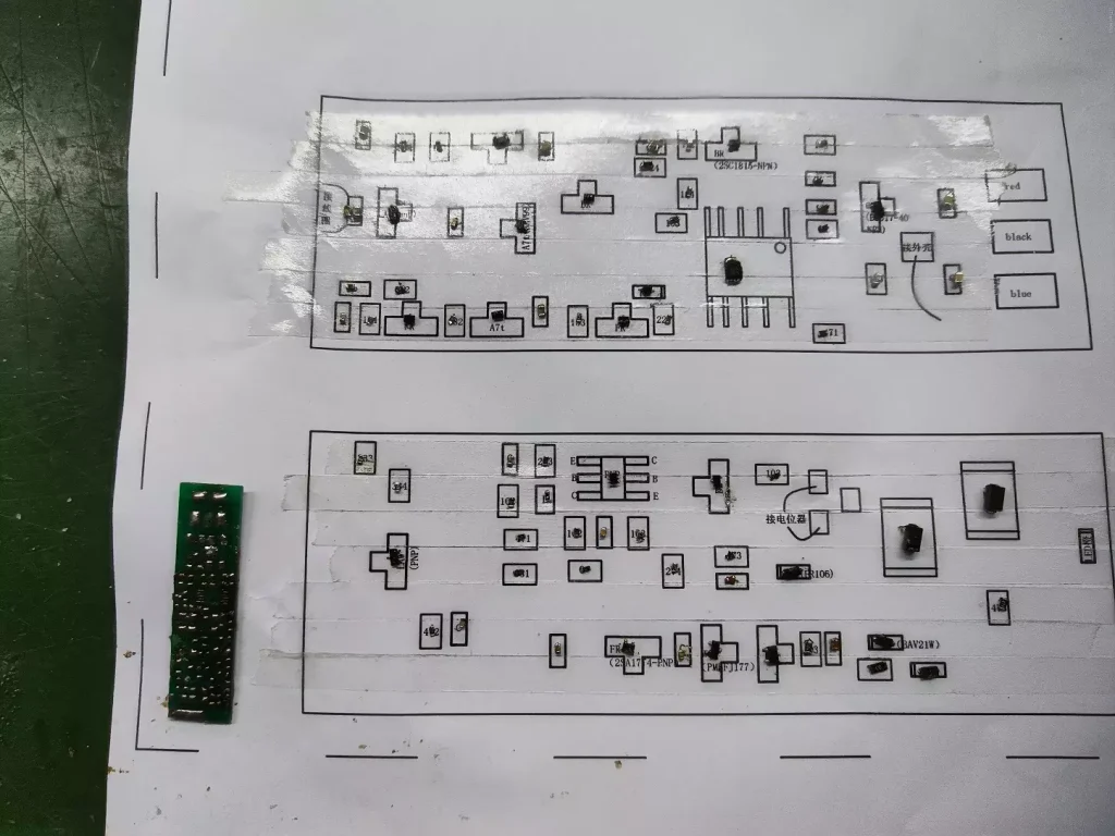
After capturing high-resolution images or scans of both sides of the board, start cataloging each component. Create a reference sheet or table that lists every resistor, capacitor, diode, transistor, IC, connector, and other relevant components. For each element, record the part number (if visible), orientation, and location on the board. ICs are particularly important, as their datasheets reveal internal pin functions, which are essential for reconstructing signal flow.
Step 4: Trace connections and nets on single and double-layer PCBs.
This is where the detective work begins — mapping copper paths into electrical nets.
Single-layer PCBs
- Visually follow traces from each component pad to the next.
- Use a continuity tester to confirm endpoints — this is essential if traces are partially obscured or corroded.
- Draw net sketches (hand-drawn or in CAD) as you go, marking each connection with its reference designators.
Double-layer PCBs
- Look for vias — small plated holes connecting traces between top and bottom layers.
- Mark each via in your images and assign an ID (e.g., V1, V2).
- Use continuity testing to confirm via connections — some may connect to internal ground or power planes.
- A lightbox or backlight can help you see through thin FR4 boards to align front and back traces visually.
Best Practices
- Always trace one net completely before moving to the next.
- Use different colors in your CAD or drawing to separate nets visually.
- Maintain a consistent ground and power labeling convention — e.g., GND always black, VCC always red.
This can be done in several ways. For simple boards, visual inspection and image overlay may be enough. In more complex designs, use a multimeter in continuity mode to verify connections. Carefully mark each net with a unique ID and track it from pin to pin, through vias, across layers, and under components. This is where high-contrast image editing or PCB CAD overlay tools can greatly improve your accuracy.

Advanced Techniques: Delayering and X-Ray Analysis
For 4-layer boards and above, visual inspection is insufficient. You need to see what is hidden inside the FR4 material.
1. Non-Destructive X-Ray Inspection (Preferred)
According to IPC standards and industry data, complex multilayer boards often require X-ray analysis for 100% accuracy regarding blind and buried vias.
- 2D X-Ray: Useful for identifying BGA ball grid arrays and checking if a via connects to an internal plane.
- 3D CT Scan: High-end labs use Computed Tomography to build a full 3D model of the internal copper layers without destroying the board.
2. Destructive Delayering (The Sanding Method)
If X-ray is unavailable, you must physically remove the FR4 dielectric material—a process known as delayering.
- Sandpaper Method: Use wet sandpaper (starts with 600 grit, finishes with 1200 grit) to gently remove the solder mask and fiberglass epoxy until the copper layer is exposed.
- CNC Milling: A precision CNC machine can remove layers with micron-level accuracy, ensuring you don’t accidentally grind away the copper traces.
- Image & Repeat: Photograph the exposed layer, then grind it away to reveal the next layer down. Software is then used to stack these images.
Step 5: Transfer the traced data into CAD software to create a schematic
Once your tracing is complete, the next step is turning that raw netlist and component log into a professional schematic.
Preparing the Workspace
- Choose your schematic capture tool (KiCad for free use, Altium or OrCAD for professional environments).
- Create a new project and set the schematic sheet size to accommodate your expected circuit complexity.
Component Placement
- Place each component symbol in the schematic according to its reference designator (R1, C1, U1, etc.).
- Use the datasheet to select the correct schematic symbol and footprint.
Net Creation
- For each net from your tracing notes, connect the corresponding pins using the software’s wiring tool.
- Keep the schematic organized by function:
- Power supply section
- Input/output section
- Signal processing section
- Control/logic section
Cross-verification
- Continuously compare the schematic with your PCB images and continuity test notes.
- Use ERC (Electrical Rule Check) in your CAD software to catch missing connections or unconnected pins.
- Label all power and ground nets clearly, ensuring they are consistent throughout.
Output and Documentation
- Once the schematic is complete, export it as a PDF and a netlist for future reference.
- Store it with your original PCB photos and component spreadsheet for a full reverse-engineering archive.
Step 6: Ensure the schematic is accurate and functional.
Even after hours of tracing, mistakes can creep in. Verification is critical.
Continuity & Resistance Checks
- Re-test key nets with your multimeter.
- Confirm there are no unintended shorts between signal lines or power rails.
Functional Group Testing
- Cross-check each circuit block (e.g., power supply, amplifier, microcontroller I/O) against known topologies from datasheets and application notes.
- If a block seems unusual, review the original PCB photos for missed vias or traces.
Simulation
- Import your schematic into a simulation tool (LTspice, Multisim) to confirm logical operation where possible.
- This helps identify incorrect polarities, swapped pins, or missing bias components.
Peer Review
- Have another engineer review your schematic.
- A second set of eyes can catch errors you’ve overlooked due to familiarity bias.

Step 7: Use KiCad and other PCB reverse engineering software to help.
Modern CAD tools can significantly accelerate the process, particularly for complex boards.
KiCad
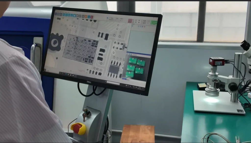
- Image Overlay: Import PCB photos into the PCB editor to align footprints visually.
- Manual Tracing: Place pads and traces over the images to replicate routing, then back-annotate into the schematic.
- Library Flexibility: KiCad’s open library system allows easy creation of custom footprints for unidentified components.

Altium Designer
- Multi-sheet Schematics: Useful for large, multi-function boards.
- 3D Visualization: Helps verify mechanical fit when recreating footprints.
- Net Connectivity Checking: Flags unconnected or incorrectly connected nets.
Specialized Reverse Engineering Software
- Some paid tools can automatically detect pads, vias, and traces from high-resolution scans.
- These are best used as assistants, not replacements for manual verification — automation can misinterpret damaged or non-standard traces.
Top PCB Reverse Engineering Software Comparison
| Software | Best For | Cost | Key Feature |
|---|---|---|---|
| KiCad | Hobbyists & SMEs | Free (Open Source) | No licensing fees, strong community plugins |
| Altium Designer | Professional Teams | Paid (Subscription) | Advanced layer management, cloud collaboration |
| Sprint-Layout | Simple Boards | Low Cost | “Tracing” background image feature |
| Target 3001! | Reverse Engineering | Paid | Specialized “Reverse Engineering” mode |
When should you use professional PCB reverse engineering services?
Sometimes, outsourcing is the smartest option.
Reasons to Outsource
- High layer count (8+ layers), where X-ray and destructive methods are needed.
- Time-critical projects where in-house engineers are busy.
- Specialized compliance where accurate documentation is required for certification.
Choosing a Service
- Look for providers with proven experience in your PCB’s domain (RF, high-speed digital, power electronics).
- Request sample reports and turnaround time estimates.
- Ensure confidentiality agreements are in place to protect IP.
How to use PCB Reverse Engineering Software effectively?
Reverse engineering software isn’t a magic button—it’s a toolset that enhances accuracy and saves time when used correctly. Once you’ve collected enough data from a physical PCB—images, component identities, and net connections—the role of software is to help you formalize that data into a structured schematic.
Most engineers start with schematic capture tools like KiCAD, EasyEDA, or Altium Designer. These platforms allow you to place components, draw connections, assign values, and simulate circuits if needed. If you’re working from scanned images or photos, some tools let you import those as backgrounds, which helps align components spatially.
In more advanced workflows, you might vectorize PCB traces using tools like AutoTrace, then convert that data into layout files. However, these processes are often messy and require heavy manual cleanup.
The key is not the software itself, but how you integrate it into your workflow. Use it to visualize logic, validate connections, and document your reconstruction—not to guess or automate what only hands-on inspection can confirm.
When should you consider PCB Reverse Engineering Services?
There are situations where outsourcing the reverse engineering process is the smarter, faster, and more cost-effective choice—especially for complex or time-sensitive projects. If you’re working with a densely packed multilayer board, high-speed signal paths, or buried components, the technical demands can quickly exceed the capabilities of an internal engineering team.
Professional PCB reverse engineering services bring access to specialized equipment like X-ray imaging, layer-by-layer milling, and proprietary analysis software. They also have standardized workflows and experienced staff trained to handle everything from military-grade boards to obsolete industrial hardware.
You might consider outsourcing if:
- Your team lacks the time or expertise for manual net tracing.
- You need an accurate schematic and Gerber files urgently.
- The project involves proprietary or sensitive board architecture.
- You’re dealing with legacy hardware and must replicate it precisely.
However, external services come with cost, lead time, and potential IP concerns. If the board is relatively simple, doing it in-house not only saves money but also builds valuable internal expertise.
Key mistakes to avoid when reverse engineering a schematic
Even experienced engineers can make critical errors. Here are the most common pitfalls and how to avoid them:
1. Misinterpreting Ground vs. Power Planes
- The Mistake: Assuming all large copper pours are Ground (GND).
- The Fix: Multilayer boards often have split power planes (e.g., 3.3V and 5V zones next to each other). Always map continuity to the regulator output pins to verify the specific voltage rail before labeling a plane.
2. Ignoring Blind and Buried Vias
- The Mistake: Assuming every hole goes all the way through the board.
- The Fix: In High-Density Interconnect (HDI) boards, a via might connect Layer 1 to Layer 2 but not visible on the bottom side. If a trace seems to “disappear,” check for buried vias using a strong backlight or X-ray.
3. Component Identification Errors
- The Mistake: Assuming a component’s value based solely on size (e.g., thinking an 0603 black component is always a resistor).
- The Fix: It could be an inductor or a ferrite bead. Always measure the component out-of-circuit or check the schematic context (e.g., is it in series with a power line?).
4. Over-reliance on Auto-Tracing Software
The Fix: Software often misinterprets scratches as traces. Manual verification is mandatory. As a rule of thumb, use automation for 80% of the work, but use human engineering for the critical 20% of logical verification.
The Mistake: Trusting “image-to-schematic” converters blindly.

Can online converters really turn PCBs into schematics?
While the idea of uploading a PCB photo and instantly receiving a complete schematic is appealing, reality is far less convenient. Most free online “PCB to schematic converter” tools are limited in capability, accuracy, and applicability. They may offer partial assistance for image vectorization or trace detection, but they cannot interpret component functions, multi-layer routing, or circuit logic.
In real-world applications—especially with multi-layer or analog boards—these tools consistently fall short. They often misinterpret pad sizes, fail to detect internal vias, and can’t identify net functionality without human input. At best, they may assist with initial layout drafting; at worst, they generate misleading or unusable output.
For accurate and professional results, reverse engineering still requires manual inspection, structured net analysis, and schematic recreation using dedicated software and engineering insight. Online shortcuts may look promising, but they are not a substitute for real reverse engineering.
Frequently Asked Questions (FAQ)
Q1: Can I reverse engineer a 4-layer PCB at home?
A1: It is difficult but possible. You can trace the top and bottom layers visually. However, determining internal connections (layers 2 and 3) usually requires destructive delayering (sanding down the board) or access to an X-ray machine, which is typically found in professional labs.
Q2: How much does professional PCB reverse engineering cost?
A2: The cost varies significantly based on complexity. A simple 2-layer legacy board might cost between $500 and $1,500, while a complex multi-layer industrial motherboard with BGA components can range from $3,000 to over $15,000 due to the need for X-ray analysis and extensive validation.
Q3: What is the difference between a Netlist and a Schematic?
A3: A Netlist is a raw text file listing all electrical connections (e.g., “Pin 1 of U1 connects to Pin 2 of R1”). A Schematic is the visual representation of these connections using standardized symbols, organized logically to show the circuit’s function (power flow, signal paths). You need a schematic to truly understand and repair the board.
Summary
Reverse engineering a PCB into a schematic is meticulous work, but with the right workflow and tools, you can create accurate documentation from any board. Start small, refine your method, and soon even complex multilayer designs will be within your reach. If you’ve faced challenges or developed your techniques, contact IWDF Solutions for help.

