

Designing a PCB for high-frequency applications is a different challenge from standard low-speed board work. The rules change, the materials change, and small layout decisions that seemed harmless at low speed can quietly break performance at GHz frequencies.
High-frequency PCB design requires careful control of materials, stackup, impedance, routing, grounding, and thermal paths. Follow these steps in the right order, and you can build reliable high-frequency hardware the first time.
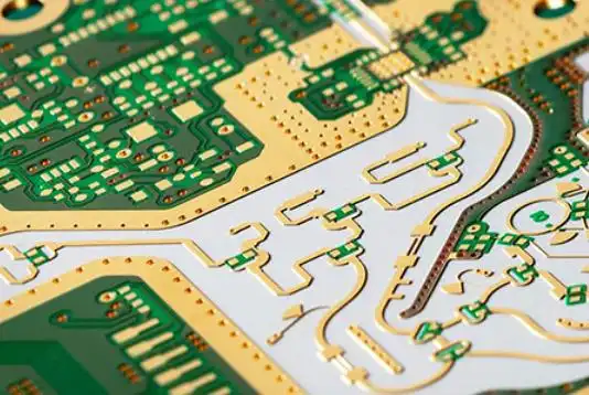
Most PCB design guides cover the basics. But when you search for “high frequency PCB design” or “PCB design rules for high frequency,” you are usually dealing with a real problem. Maybe your Wi-Fi board has poor range. Maybe your radar module fails EMC. Maybe you are about to start a 5G or automotive project and you are not sure where to begin. This guide walks through every step in a logical order — from what a high-frequency PCB actually is, through material choice, stackup, routing, grounding, thermal design, and finally how to choose the right manufacturing partner. Each section answers a specific question that engineers, managers, and sourcing teams actually ask.
What Is a High-Frequency PCB?
High-frequency PCBs are specialized circuit boards designed to transmit signals from 100 MHz up to 100 GHz. They use materials with low dielectric constants and low loss factors to ensure minimal signal loss, minimal impedance mismatch, and stable performance across frequency. They are essential for any high-speed wireless or data application where signal quality directly determines whether the product works.
What makes them different from a standard PCB?
A standard FR4 board carries signals between components. A high-frequency PCB must also control how those signals travel. At high frequency, three things happen that do not matter at low speed:
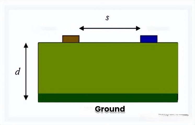
- Traces become transmission lines. A copper trace is no longer just a wire. Its width, thickness, and distance from the reference plane all determine its impedance. Any mismatch between that impedance and the connected components causes reflections that degrade the signal.
- The dielectric material absorbs energy. Standard FR4 has a dissipation factor (Df) of around 0.020 at 10 GHz. That means a significant portion of your signal turns into heat inside the board material. Specialized RF laminates bring that number down to 0.001–0.004, which can mean five to ten times less signal loss over the same trace length.
- The return current path matters. At low speed, return current spreads across the ground plane in any convenient path. At high frequency, return current concentrates directly under the signal trace. Any break in that path — a slot, a gap, a missing ground plane — forces current to detour, which creates noise, crosstalk, and EMI.
Where are high-frequency PCBs used?
| Application | Frequency Range |
|---|---|
| Bluetooth | 2.4 GHz |
| Wi-Fi 5 | 2.4 / 5 GHz |
| Wi-Fi 6E / 7 | 2.4 / 5 / 6 GHz |
| 5G Sub-6 GHz | ~3.5 GHz |
| 5G mmWave | 24–40 GHz |
| Automotive short-range radar | 24 GHz |
| Automotive long-range radar | 77 GHz |
| Ku-band satellite | 12–18 GHz |
| Ka-band satellite | 26–40 GHz |
Understanding what a high-frequency PCB is sets the foundation for every decision that follows. The next question — when do you actually need one — is equally important.
When Do You Actually Need High-Frequency PCB Design Rules?
You need high-frequency PCB design rules when your trace length approaches one-tenth of the signal’s wavelength inside the board material. At that point, the trace starts to behave as a transmission line and standard wiring assumptions no longer hold.
A simple way to decide
You do not need a complex calculation. Use this practical test:
- Find the highest frequency your board must handle — including harmonics of clocks, not just the carrier.
- Calculate the wavelength at that frequency inside your PCB material: wavelength = speed of light ÷ (frequency × √Dk).
- If your longest critical trace exceeds one-tenth of that wavelength, apply high-frequency rules.
For most teams, the answer is: if you are working above 500 MHz, apply high-frequency rules. If you are above 1 GHz, you have no choice.
Why start early?
Applying high-frequency rules late in the design is expensive. It means changing trace widths, which may change the stackup. Changing the stackup may mean changing the material. Changing the material changes costs and lead times. It is far cheaper to design for high frequency from the start than to rework a finished layout.
This is also why the first two steps of any high-frequency design are always: understand what kind of board you are building, then lock your electrical requirements before touching the schematic or layout. Those requirements drive every material and stackup decision that follows.
Step 1: Select the Material Comes First in High-Frequency PCB Design
Before you draw a single trace, you need to know what the board is made of. This is not a detail you can decide later. Material choice determines trace width, stackup thickness, maximum loss, and manufacturing process. Everything else is built on top of it.
You choose PCB materials based on their dielectric constant (Dk), dissipation factor (Df), and thermal properties — matched to your operating frequency, signal loss budget, and environment.
The three properties that drive material choice
Dielectric constant (Dk)
Dk controls how fast signals travel through the material and how wide your traces must be to hit a target impedance. Lower Dk gives you wider traces for the same impedance, which can be easier to manufacture. More critically, Dk must stay stable across frequency and temperature. A material whose Dk shifts with temperature makes field impedance control unreliable in real-world conditions.
Dissipation factor (Df)
Df is the single most important number for signal loss. A high Df means the dielectric converts RF energy into heat. Standard FR4 has a Df of about 0.020–0.025 at 10 GHz. Low-loss RF laminates like Rogers RO4350B sit at around 0.0037. PTFE-based laminates can reach 0.001. The difference is not subtle — at 10 GHz, you can lose five to ten times more signal on FR4 than on a proper RF laminate over the same trace length.
Thermal properties
RF boards with power amplifiers or radar modules run warm. You need to check: thermal conductivity (how well the material moves heat), CTE or coefficient of thermal expansion (must match copper to prevent via failure), and glass transition temperature Tg (the point where the material starts to soften under heat).
Material comparison table
| Material | Dk | Df at 10 GHz | Cost vs. FR4 | Best Use |
|---|---|---|---|---|
| Standard FR4 | 4.2–4.7 | 0.020–0.025 | 1× | Below ~1 GHz |
| Low-loss FR4 | ~3.7–4.0 | 0.010–0.015 | 1.5–2× | High-speed digital, a few GHz |
| Rogers RO4350B | ~3.48 | ~0.0037 | 3–4× | 2–10 GHz, Wi-Fi, 5G Sub-6 |
| Rogers RO4003C | ~3.38 | ~0.0027 | 3–4× | General RF 1–20 GHz |
| Rogers RO3003 | ~3.00 | ~0.001 | 5–6× | mmWave 5G, Ka-band |
| PTFE laminates | 2.1–2.6 | ~0.001 | 4–8× | Radar, satellite, aerospace |
| LCP | ~2.9–3.2 | 0.002–0.004 | 4–6× | Flexible RF, antenna-in-package |

How to pick the right material for your project?
- 2.4–5 GHz (Wi-Fi, Bluetooth, Sub-6 5G): Short RF traces may work on good low-loss FR4. Longer RF feed lines or tight link budget specs need Rogers RO4350B or a similar laminate.
- 10–20 GHz (MIMO, point-to-point links): Use RO4003C or equivalent. FR4 adds too much loss at these frequencies.
- 24–77 GHz (automotive radar, mmWave 5G): Use Rogers RO3003, Taconic RF-35, or PTFE. No practical alternative exists.
- Mixed boards (RF + digital + power): Use hybrid stackups. Put RF cores on a low-loss laminate. Put digital and power layers on standard material to control cost.
Why this is Step 1: You cannot design a stackup without knowing the material thickness options your factory stocks. You cannot calculate trace width without knowing Dk. You cannot estimate signal loss without knowing Df. Confirm your material choice with your PCB manufacturer before you do anything else. Some laminates have long lead times or limited stocking. Finding that out early saves weeks.
Step 2: Plan a High-Frequency PCB Stackup
Material selection tells you what the board is made of. Stackup planning tells you how the layers are arranged. This is Step 2 because trace widths, impedance calculations, and routing rules all depend directly on the stackup. You cannot calculate a 50 Ω trace width until you know the dielectric thickness under that trace.
A good high-frequency stackup places a solid reference plane next to every RF or high-speed signal layer, separates noisy digital sections from sensitive RF sections, and uses symmetric layer ordering to prevent warping in fabrication.
The three rules every stackup must follow
Rule 1: Every RF or high-speed signal layer needs an adjacent reference plane.
The plane provides the return current path and sets the characteristic impedance. Without it, you have no controlled impedance and no predictable signal behavior.
Rule 2: The stackup must be symmetric.
Asymmetric stacks warp during lamination. Warping creates uneven dielectric thickness across the panel, which shifts impedance values away from your targets and makes production consistency very difficult.
Rule 3: Isolate RF from digital.
Digital switching creates broadband noise. Placing a digital signal layer directly adjacent to an RF layer invites that noise into your sensitive receive chains. Separate them with at least one solid plane.
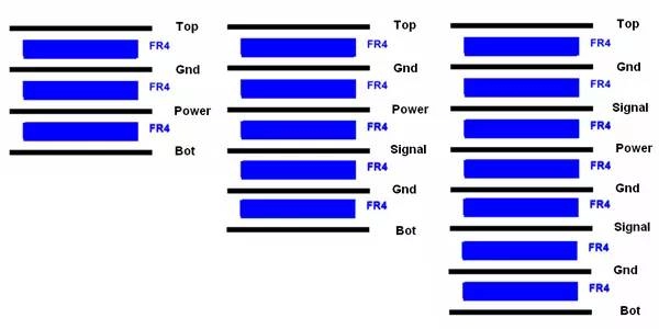
Practical stackup examples
4-layer stack for Wi-Fi / Sub-6 5G / basic RF:
| Layer | Role |
|---|---|
| L1 | RF and high-speed signals (microstrip over L2) |
| L2 | Solid ground plane |
| L3 | Power distribution |
| L4 | Control and low-speed signals |
RF signals on L1 sit directly above solid ground on L2. This gives clean, predictable impedance and a short return path. Digital control signals go to L4, far from the RF layer.

6-layer stack for stricter EMI or higher routing density:
| Layer | Role |
|---|---|
| L1 | High-speed and RF (microstrip) |
| L2 | Ground plane |
| L3 | Internal signal (stripline between L2 and L4) |
| L4 | Power plane |
| L5 | Ground plane |
| L6 | Low-speed signals |
L3 is stripline — fully enclosed between two planes. This gives better shielding and lower radiation than microstrip. L1 and L6 remain as microstrip for easy access to connectors, antennas, and test points.
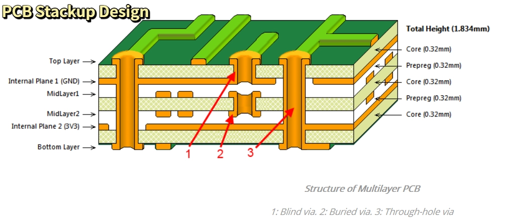
For designs at 24–77 GHz, 8–12 layer stacks with blind and buried vias are common. The extra layers are not about routing complexity. They are about giving every critical signal the reference plane it needs while keeping RF trace lengths as short as possible.
Why stackup comes before routing: Once the stackup is fixed — materials, layer count, dielectric thicknesses — you can calculate the exact trace width that hits your impedance target on each layer. Only then does it make sense to start routing. Routing before the stackup is locked means rerouting everything when the stackup changes.
Step 3: Control Impedance — The Core of High-Frequency PCB Design
You have chosen your materials. You have a stackup with defined dielectric thicknesses. Now you need to calculate the exact trace geometries that give you controlled impedance. This is Step 3, and it is the most critical technical decision in the entire design.
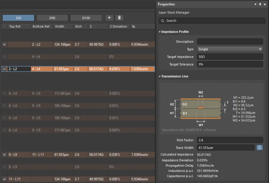
Impedance mismatch causes reflections. Reflections reduce signal amplitude, distort waveforms, and increase error rates. For RF systems, even a small mismatch can push a design below its minimum range or link budget. Controlled impedance means every critical trace has a characteristic impedance that matches the system requirement — typically 50 Ω for single-ended RF lines, and 90–100 Ω for differential pairs.
What determines a trace’s impedance?
Four factors set the characteristic impedance of any trace:
- Trace width — wider trace means lower impedance
- Trace thickness — thicker copper slightly lowers impedance
- Dielectric height — the distance from the trace to the reference plane; thinner means lower impedance
- Dielectric constant Dk — higher Dk means lower impedance
You do not calculate these by hand for production. You use the impedance calculator in your PCB design tool. Enter your stackup parameters — the numbers your manufacturer has confirmed. Adjust the trace width until the tool shows your target impedance. Lock that width in your design rules.
Common impedance targets by signal type
| Signal Type | Standard Impedance Target |
|---|---|
| RF single-ended | 50 Ω |
| Video (coax-style traces) | 75 Ω |
| USB differential pairs | 90 Ω |
| PCIe / Ethernet differential | 100 Ω |
What your manufacturer must provide?
Your PCB factory should:
- Confirm the exact stackup and simulate impedance before production
- Include test coupons on every production panel
- Measure those coupons after fabrication and provide a report
If a factory cannot or will not provide impedance test reports, treat that as a serious warning sign for high-frequency work.
A note on solder mask
Many designers forget that solder mask adds 2–3 Ω to a microstrip trace. If your target is 50 Ω and you cover the trace with standard solder mask, the real impedance will be lower. Either account for this in your trace width calculation, or specify in your fab notes that the solder mask must be removed over critical RF traces. This small detail causes more first-prototype failures than most engineers expect.
Insertion loss: how to keep it low
Signal loss along a trace comes from three sources:
| Loss Type | Main Cause | How to Reduce It |
|---|---|---|
| Dielectric loss | High Df of substrate | Use a low-Df laminate matched to your frequency |
| Conductor loss | Skin effect and rough copper surface | Short traces, smooth copper foil |
| Radiation loss | Poor layout, plane gaps, sharp corners | Solid ground planes, careful routing |
At 10 GHz, a well-designed trace on Rogers RO4350B loses roughly six to eight times less power per centimeter compared to the same trace on standard FR4. At 28 GHz, FR4 is not a realistic choice for any main RF path.
Step 4: The Routing Rules That Make or Break a High-Frequency Layout
You have the right material, the right stackup, and the correct trace widths for your target impedance. Now comes routing. This is Step 4 — and the order matters. You route after impedance is defined because routing uses the trace widths and layer assignments set in the previous step.
High-frequency routing keeps traces short and direct, maintains controlled geometry along the full trace length, gives every signal a clean return path, and prevents electromagnetic coupling between adjacent signals.
The rules that matter most
Keep traces short. Every extra millimeter adds loss and delay. Route components in the order they appear in the signal chain. Bring antennas, amplifiers, filters, and connectors as close together as physically possible without violating thermal and assembly clearances.
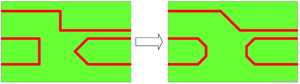
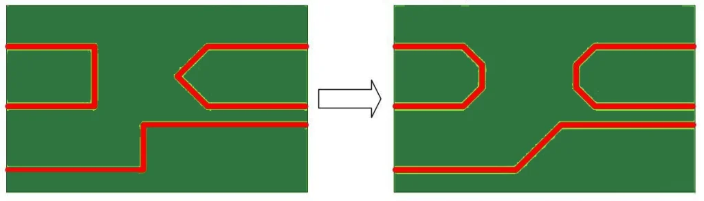
No 90-degree corners. A sharp corner slightly concentrates current and disturbs impedance at the bend point. Use two 45-degree bends or a smooth arc instead. This is a small effect at 2.4 GHz but becomes meaningful at 24 GHz and above.
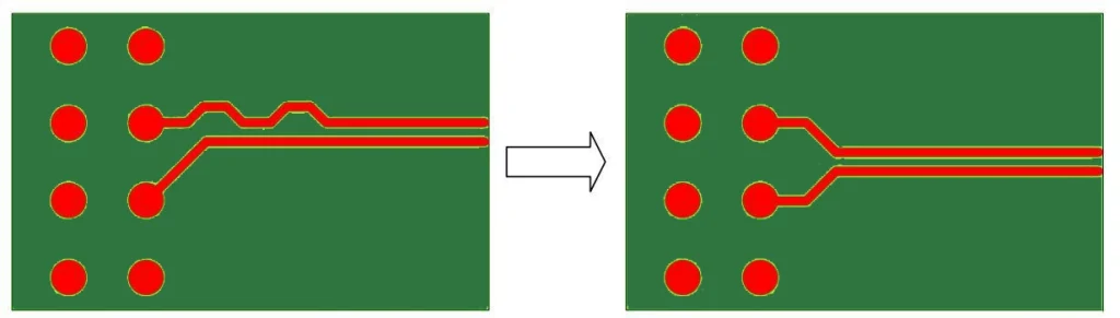
The 3W spacing rule. Keep the center-to-center distance between parallel high-frequency traces at least three times the trace width. This limits electromagnetic coupling between them. For very sensitive receive paths, use 5W or add a grounded guard trace between the signals.

Never route across a ground plane split. When a trace crosses a slot or gap in its reference plane, the return current takes a long detour around the gap. That long loop picks up noise and radiates. It also breaks impedance continuity. This single mistake is responsible for more EMC test failures than almost any other layout error.
Route RF components in signal flow order. Place the antenna, LNA, filter, mixer, and amplifier in the physical order that matches the schematic signal chain. Short, straight connections between them prevent long trace detours.
Differential pair routing rules
| Rule | Why It Matters |
|---|---|
| Keep spacing constant along the full length | Any width change disturbs differential impedance |
| Match lengths within your tool’s tolerance | Mismatch creates timing skew and degrades common-mode rejection |
| Avoid layer changes when possible | Each via adds parasitics and potential mismatch |
| Route both traces simultaneously in your CAD tool | Ensures they follow identical paths |
Step 5: Via Design and Ground Plane Integrity
Routing deals with traces. But traces are only part of the signal path. Vias carry signals between layers, and the ground plane carries every return current. Both deserve the same care as the traces themselves. This is Step 5 because the via design and ground integrity depend on the stackup and routing decisions already made.
Poor via design introduces parasitic inductance, capacitance, and stub resonances. A damaged or incomplete ground plane forces return currents onto long, noisy paths. Together, these problems can ruin a design that looks perfect on the routing layer.
Via design rules for RF work
Minimize vias on RF signal paths. Each via on a critical trace adds roughly 0.1–0.2 dB of loss at 10 GHz. More seriously, the unused portion of a through-hole via forms a stub. When that stub reaches a quarter wavelength at your operating frequency, it resonates and creates a sharp dip in signal level at exactly that frequency. This is called stub resonance, and it is invisible in layout but deadly in measurement.
Solutions to stub resonance:
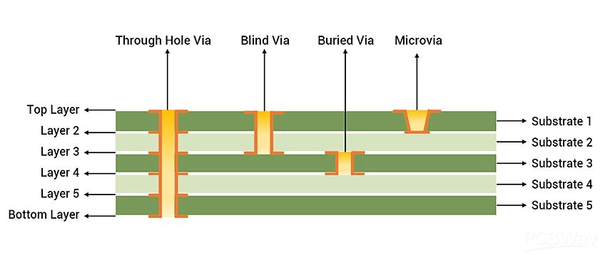
- Back-drilling: After fabrication, drill out the unused stub portion from one side. Common for PCIe, high-speed SerDes, and 10+ GHz RF.
- Blind vias: Connect only the layers you need, starting from one outer surface.
- Buried vias: Connect inner layers without passing through the outer copper layers at all.
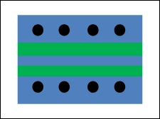
Use via fences. A line of ground vias around RF traces, along board edges, or around RF blocks creates an electromagnetic barrier. Keep via spacing at less than one-tenth of the wavelength at your highest frequency. For a 10 GHz design on Rogers RO4350B (wavelength ~17 mm), that means via fences spaced no more than about 1.7 mm apart.
Ground plane rules
| Practice | Why It Matters |
|---|---|
| Keep at least one full, unbroken ground plane layer | Provides stable return path for all high-frequency currents |
| Never cut the ground plane under RF traces | Plane cuts force return current to detour, creating noise and impedance breaks |
| Join split grounds at exactly one point | Prevents ground loops between analog and digital sections |
| Place decoupling capacitors with very short connections to IC power and ground pins | Long connections reduce decoupling effectiveness at high frequency |
Step 6: Power Delivery and Thermal Management
A board that routes well and has perfect ground planes can still fail if the power delivery is noisy or if heat builds up in RF components. This is Step 6 because it is the last major design discipline before verification and manufacturing. It runs in parallel with routing but depends on the component placement decisions made in previous steps.
Power delivery network basics
Every fast IC needs local decoupling between its power pin and ground. The closer the capacitor is to the pin, the more effective it is. A capacitor placed 10 mm away from a power pin is far less effective at high frequencies than one placed 1 mm away.
Use multiple capacitor values in parallel near each fast device: for example, 100 nF + 10 nF + 1 nF. Each value filters a different frequency range. One capacitor value cannot cover the full spectrum of a modern high-speed IC.
Keep power planes broad and solid. Where possible, run power and ground planes adjacent to each other. This creates distributed capacitance across the board, which supplements the discrete decoupling capacitors.
Thermal management steps
| Step | Practical Action |
|---|---|
| Estimate heat sources | Check worst-case power dissipation of PA, converters, and processors |
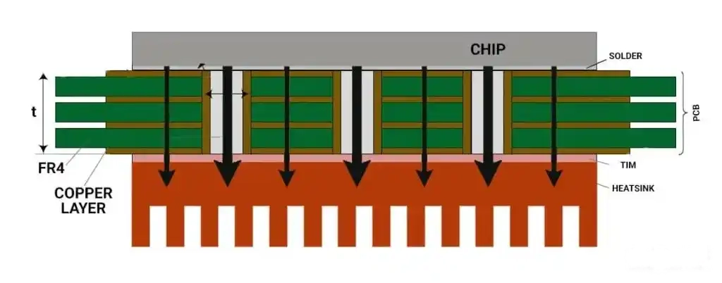
| Add thermal vias | Place via arrays under hot packages to move heat to inner copper planes or the board back |
| Use copper pours as heat spreaders | Large copper areas on inner layers distribute heat away from concentrated sources |
| Separate hot and cold components | Keep power amplifiers away from temperature-sensitive sensors |
| Plan system-level cooling | Consider heatsinks, thermal interface pads, and airflow as part of the full system design |
A 77 GHz radar module running at several watts in a sealed housing will overheat without a deliberate thermal path. Thermal design is not optional for high-power RF products.
Step 7: Simulation, Testing, and DFM Review Before Production
You have gone through materials, stackup, impedance, routing, vias, grounding, power, and thermal. Before you send files to the factory, one more step is necessary: verification. Simulation catches design problems before fabrication. Physical testing on prototypes confirms the design works in the real world. A DFM review ensures the factory can actually build what you designed.
Useful simulation tools by task
| Tool | Primary Use |
|---|---|
| Ansys HFSS | 3D electromagnetic simulation: antennas, via structures, connectors |
| Cadence Sigrity / Clarity | Signal integrity and power integrity analysis |
| Keysight ADS | RF circuit and system-level simulation |
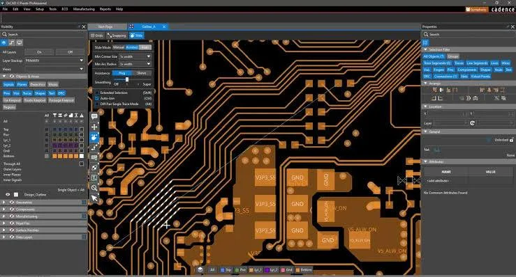
| Altium Designer (built-in) | Impedance calculation, length matching, basic SI checks |
| HyperLynx (Siemens) | Signal integrity, crosstalk, and EMI analysis |
For a 2.4 GHz Wi-Fi board, built-in tool calculations plus careful layout may be sufficient. For a 77 GHz radar module, full 3D EM simulation of critical via structures and feed lines is necessary before committing to prototype fabrication.
Physical tests for prototype boards
- TDR (Time Domain Reflectometry): Measures impedance along a trace. Immediately shows where mismatches or discontinuities are.
- VNA (Vector Network Analyzer): Measures S-parameters — insertion loss, return loss, and isolation. Essential for any RF path verification.
- Near-field scanning: Maps EMI across the board surface to find hot spots that are invisible in simulation.
- Eye diagram: Checks signal quality at the receiver for high-speed serial links.
DFM review checklist before submitting to the factory
| Item | Why It Matters |
|---|---|
| Confirm material availability and lead time | Some laminates are not stocked and need weeks of lead time |
| Mark all controlled-impedance traces clearly in fab notes | The factory needs to know which traces to verify |
| Specify solder mask removal over RF traces if needed | Solder mask changes impedance by 2–3 Ω |
| Include impedance test coupon design on the panel | Coupons let the factory verify impedance without cutting production boards |
| Request the factory’s DFM analysis before approving production | Catches issues that are cheap to fix in design but expensive to fix in fabrication |
How Do You Choose the Right High-Frequency PCB Partner in China?
Many European and North American teams look to China for PCB design, fabrication, and assembly. China handles a significant share of global PCB production, and Shenzhen in particular has a concentrated ecosystem of factories and design houses. You choose a high-frequency PCB partner based on specific technical capabilities, engineers PCB design experience, factory’s relevant certifications, and the quality of their engineering communication — not price alone.
Questions to ask before sending your files
- Which RF laminates do you stock? (Rogers, Taconic, PTFE, LCP?)
- Can you share a real stackup example for 5 GHz or 24 GHz?
- What impedance tolerance can you reliably hold — ±10%, ±5%, or ±3%?
- Do you support back-drilling, blind vias, and buried vias?
- Do you offer PCB design services, not just fabrication?
- Can you handle PCB reverse engineering from a physical board sample?
A strong partner gives concrete answers with real examples. A weak partner sends only a price sheet.
Certifications that matter for B2B work
| Certification | When You Need It |
|---|---|
| ISO 9001 | Every serious B2B application |
| IATF 16949 | Automotive products |
| AS9100 | Aerospace and defense |
| ISO 13485 | Medical devices |
| RoHS / REACH | Products sold in Europe |
| UL certification | Products sold in North America |
How to evaluate a supplier quickly?
| Factor | Strong Partner | Weak Partner |
|---|---|---|
| Material knowledge | Names specific laminates and confirms stocking | Mentions only FR4 |
| Engineering support | Engineers reply to technical questions directly | Only sales staff respond |
| Impedance process | Provides test coupon data and written reports | Cannot explain how they check impedance |
| Services offered | Design, reverse engineering, fabrication, PCBA, testing | Bare boards only, no engineering support |
| Communication | Clear, fast, honest about lead times and risks | Slow, vague, avoids technical questions |
For overseas B2B teams, a one-stop service provider that handles PCB design, PCB reverse engineering, fabrication, and assembly under one roof removes significant coordination overhead. Fewer handoffs between vendors means fewer misunderstandings and faster delivery.
Frequently Asked Questions
Q1: What frequency counts as high frequency in PCB design?
Most engineers treat signals above 500 MHz as high frequency. Above 1 GHz, traces must be treated as transmission lines where impedance, loss, and return paths are active design concerns. Above 2.4 GHz, standard FR4 starts to cause measurable signal loss on all but the shortest traces.
Q2: Can I use FR4 for a high-frequency PCB?
You can use FR4 for some designs up to about 1–2 GHz, especially when RF traces are short and link budget margins are generous. Above that, the dissipation factor of FR4 causes too much insertion loss for practical RF work. Low-loss laminates like Rogers RO4350B are needed for most designs above 2 GHz.
Q3: Why does controlled impedance matter so much?
At high frequency, any mismatch between a trace’s characteristic impedance and the connected component causes reflections. Those reflections reduce signal amplitude, distort waveforms, and increase bit error rates in digital links or reduce link margin in RF systems. Controlled impedance ensures signals travel through the board without unwanted reflections.
Q4: Why is the ground plane so important in high-frequency PCB design?
The ground plane carries the return current for every high-frequency signal on the board. A solid, unbroken plane keeps that return path short and the current loop area small. A slot or gap forces return current onto a long detour, which creates EMI, crosstalk, and impedance discontinuities.
Q5: What is the 3W rule?
The 3W rule states that the center-to-center distance between two parallel high-frequency traces should be at least three times the trace width. This limits electromagnetic coupling between them to an acceptable level for most designs. For more sensitive lines, use a 5W spacing or add grounded guard traces.
Q6: How many layers does a high-frequency PCB need?
Simple RF modules at 2.4–5 GHz often work well on 4 layers. Designs with mixed signals, stricter EMI requirements, or operating frequencies above 10 GHz typically need 6–12 layers. Layer count is determined by how many solid reference planes each signal layer needs — not by complexity for its own sake.
Q7: What is a via stub and why does it cause problems?
A via stub is the unused portion of a through-hole via that extends beyond the connected layers. At high frequency, this stub acts as a short transmission line. When its length equals a quarter wavelength at the operating frequency, it resonates and creates a sharp dip in signal level. Back-drilling or using blind and buried vias eliminates the stub.
Q8: What certifications should a Chinese PCB factory have for serious B2B work?
The minimum is ISO 9001 for quality management. Automotive projects need IATF 16949. Aerospace and defense applications require AS9100. Medical products need ISO 13485. Products sold in Europe need RoHS and REACH compliance. Always verify that certificates are current and issued by a recognized third-party body.
Q9: Can a Chinese PCB factory help with PCB reverse engineering of high-frequency boards?
Some specialized factories and design houses in China offer PCB reverse engineering. They can scan an existing board, recreate the schematic and layout, and optimize the design for higher frequencies, better EMC performance, or more efficient volume manufacturing. This is especially useful when original design files are lost or when upgrading a legacy RF product.
Q10: When do I actually need EM simulation for high-frequency PCB design?
For boards below 5 GHz with simple, short RF paths, careful rule-based layout combined with impedance calculation tools is often enough. For frequencies above 10 GHz, complex via structures, antenna integration, or any project where a single prototype spin is very costly, EM simulation is worth the time and tool investment. It is always cheaper to fix a problem in software than to build two or three extra prototype runs.
Conclusion
High-frequency PCB design follows a clear order for a reason. Each step depends on the one before it. You start by understanding what a high-frequency PCB is and when those design rules apply. Then you choose materials, because every other calculation rests on Dk and Df values. You plan the stackup next, because trace widths and layer assignments follow directly from it. Then you define impedance and routing rules, design your via structures and ground planes, manage power and heat, and verify the design before production. Skip a step or reverse the order, and problems appear in the lab that are expensive and slow to fix. Follow this sequence, work with a manufacturing partner who genuinely understands high-frequency PCB design and PCB reverse engineering, and you will move from concept to working hardware with far fewer surprises. Contact IWDF Solutions if you need high frequecy proejct.

