
Building your first hardware product is thrilling, but the path to a functional PCBA prototype is paved with potential setbacks. As a first-time founder, you’re likely grappling with essential questions: How many PCB layers do we need? How do we avoid costly assembly errors? What DFM pitfalls could derail our schedule? Without a clear plan, these uncertainties can lead to functional failures, manufacturing delays, and budget overruns that strain your resources.
This 7-step PCBA prototype checklist is designed to guide you from concept to a production-ready build. It covers critical phases: defining your requirements, schematic and layout design, BOM validation, DFM/DFT review, preparing manufacturing files, overseeing assembly and testing, and planning your iteration for ramp-up. By following this structured approach, you’ll eliminate ambiguity, communicate more effectively with manufacturers, and drastically reduce the risk of expensive revisions.
Quick Summary: 7 Essential PCBA Prototype Steps
Before diving into the detailed breakdown, here’s a concise overview of the seven critical phases:
- Clarify Product Requirements and Prototype Scope – Define whether you’re building an MVP functional prototype, a performance validation version, or a near-production design that will guide cost and timeline decisions.
- Design Schematic, PCB Stack-up and Manufacturable Layout – Create a modular schematic with proper power and clock distribution, select appropriate PCB layer count and impedance control, and layout components with manufacturing constraints in mind.
- Validate BOM, Component Availability and Cost Targets – Verify component specifications, source alternatives for obsolete or unavailable parts, and establish realistic cost targets that scale from prototype to mass production.
- Run DFM/DFT Review with Your PCBA Partner – Conduct design-for-manufacturability and design-for-test checks to identify spacing violations, testing limitations, and assembly risks before any fabrication begins.
- Prepare Complete PCBA Prototype Files Package – Compile all necessary manufacturing files, including Gerber layers, assembly drawings, BOM, manufacturing notes, and test specifications in a standardized format.
- Prototype Assembly, Bring-Up and Functional Testing – Execute first-piece inspection, perform controlled power-up procedures, and validate basic functionality before declaring the prototype ready for engineering evaluation.
- Iterate, Document and Prepare for Pilot Production – Record all design changes, establish a clear version history, and transition proven prototype designs into pilot production configurations using the same supply chain and manufacturing processes.
Step 1: Clarify Product Requirements and Prototype Scope
Understanding Your Prototype’s True Purpose
The first decision—and often the most consequential—is determining what “done” looks like for your prototype. Many hardware teams skip this step or rush through it, only to discover halfway through design that their prototype misaligns with their actual goals.
Checkpoints: Define Your Prototype Type
Your prototype should fit into one of three primary categories, each with distinct implications for design decisions, manufacturing approach, and timeline:
Functional MVP (Minimum Viable Product)
This is your proof-of-concept. You’re testing core functionality—Does the wireless connection work? Can the sensor read accurate data? Does the algorithm process inputs as expected? For this prototype, you typically accept single-layer or double-layer PCBs, hand-soldered components in critical areas, and minimal automated testing. A functional MVP often requires 2-4 weeks from design freeze to working hardware.
Performance Validation Prototype
Here you’re validating electrical characteristics: power consumption, thermal behavior, signal integrity under load, and compliance margins. This prototype needs proper layer count for impedance control, complete assembly (no hand-soldering shortcuts), and comprehensive electrical testing. You should use components and footprints intended for production, not development boards or breakout modules. Timeline typically extends to 4-8 weeks.
Near-Production Prototype (Pilot-Ready)
This is your bridge to mass production. You’re testing the actual assembly process, verifying manufacturing yields, validating supply chain feasibility, and confirming that your design works at the scale you’ll use for pilot batches. This prototype must follow all production design rules, undergo full DFM review, and include statistical process control. Budget 6-12 weeks and treat this as your first genuine production run at small volume.
Checkpoints: Define Electrical and Performance Specifications
Beyond prototype type, you need clear electrical boundaries:
- Power specifications: Supply voltage range (e.g., 3.3V ±10%), current consumption budget, and whether battery power, USB power, or industrial supply will be used.
- Signal specifications: Highest clock frequency, any high-speed interfaces (DDR memory, Ethernet, PCIe), and signal integrity requirements.
- Interface definitions: USB versions, wireless standards (Bluetooth 5.0, Wi-Fi 6, Cellular), industrial protocols (CAN, Modbus), and mechanical connectors.
- Environmental range: Operating temperature (-20°C to +60°C is common for consumer; wider ranges for automotive/industrial), humidity exposure, and any mechanical shock or vibration.
- Regulatory pathway: Early identification of required certifications (FCC Part 15 for RF emissions in North America, CE marking in Europe, RoHS compliance) influences component selection and design constraints.
Checkpoints: Establish Production Volume Expectations
This question determines material choices, component packaging, and manufacturing process:
- 100-500 units: Hand-placed components, manual solder paste application, and rework-tolerant designs are feasible. Single-sided or two-sided assembly with selective hand-soldering of dense areas.
- 500-5,000 units: Full automated assembly with surface-mount and selective through-hole components. Standard PCB materials, mid-range component packages, and standard lead times.
- 5,000-50,000 units: Optimized for production efficiency—bulk component pricing, specialized packaging to reduce assembly time, and potential for parallel production lines.
- 50,000+ units: Custom component solutions, optimized supply chain negotiations, and potentially custom package designs. Manufacturing becomes a competitive advantage.
Even if you’re only building 10 prototypes today, identifying your target volume range allows you to design with scalability in mind. This prevents costly redesigns once you approach production volumes.
Common Mistakes at This Stage
- Scope creep without boundaries: Launching design without freezing feature set, leading to mid-design requirement changes that cascade into timeline delays.
- Over-specifying the prototype: Designing for full production capability when an MVP would validate core assumptions faster and cheaper.
- Ignoring component lead times: In 2024-2025, some specialty components have 20-40 week lead times. Ignoring this during requirement definition can halt your entire project.
- Vague interface definitions, such as “wireless connectivity” without specifying Bluetooth, Wi-Fi, or cellular, lead to completely different design approaches.
IWDF Solutions Tips
We’ve helped dozens of first-time founders clarify their prototype scope through structured requirements review calls. We ask specific questions about your target volume, production timeline, and acceptable trade-offs between cost and performance. We then provide a written requirements summary that serves as your design foundation—preventing misalignment between your team’s vision and the reality of manufacturing. This consultation is complimentary for potential PCBA partners and typically saves 2-3 weeks of wasted design effort.
Step 2: Design Schematic, PCB Stack-up, and Manufacturable Layout
Why Design Quality Determines Prototype Success
A schematic designed for hobbyist breadboards won’t work reliably in a real PCBA assembly. The difference between a prototype that works intermittently and one that works consistently often comes down to careful attention to power distribution, impedance control, and manufacturing-aware layout. Many hardware engineers learn this painfully through prototype iterations.
Schematic Design: Build for Reliability, Not Just Function
Power Tree Architecture
Your schematic should clearly show the power distribution hierarchy. Start with your primary input (USB, battery, or industrial supply), then show each voltage rail and its regulation chain. For example:
- Primary input → Main regulator (5V) → Secondary regulators (3.3V, 1.8V, analog 3.3V)
- Each rail should be independently decoupled with appropriate capacitor values calculated for your current demands and switching frequencies.
- Bypass capacitors near power pins of ICs (0.1 µF ceramic is standard for digital; add 10-100 µF electrolytic for bulk storage depending on load transients).
This architecture makes troubleshooting power supply issues straightforward. When something doesn’t work on your prototype, a clear power tree lets you methodically verify each rail.
Clock and Signal Distribution
If your design includes microcontrollers, microprocessors, or high-speed interfaces (DDR, Gigabit Ethernet, USB 3.0), dedicate significant schematic attention to clock trees and signal conditioning:
- Oscillators should be placed close to consuming ICs with dedicated power supplies (separate regulator or carefully filtered rail).
- High-speed signals need to follow trace length rules and impedance specifications defined in IC datasheets.
- For designs with multiple clock domains, use clear labeling (CLK_MCU, CLK_DDR, etc.) to prevent layout confusion.
Peripheral Circuit Design
Around each major IC—microcontroller, wireless module, sensor—follow the exact schematic recommendations in the IC datasheet. Don’t assume your engineering intuition is better than IC vendor recommendations. They’ve tested thousands of designs; you’ve tested a few. This is where many hobbyist designs fail at scale: they deviate from datasheet recommendations, expecting to save board space or component cost.

PCB Stack-up: Choose the Right Layer Count
Layer count is one of the most cost-impactful decisions. Choosing wrong wastes money; choosing right unlocks performance.
2-4 Layer PCBs: When Suitable
Use for simple functional prototypes with low-speed digital signals, basic analog circuits, or hand-soldered designs. Layer count:
- 2-layer: Single power plane, single ground plane (or mixed signal/ground sharing). Suitable for 5-10MHz maximum speeds and low-density component placement.
- 4-layer: Dedicated power plane and ground plane, two signal layers. Suitable for 50-100MHz designs, moderate component density.
2-layer PCBs cost 30-40% less than 4-layer PCBs, but signal integrity and EMI performance suffer. Choose a 2-layer only if noise immunity isn’t critical.
6-8 Layer PCBs: Standard for Performance Prototypes
6-layer structure: Signal-Ground-Power-Power-Ground-Signal allows excellent return path control, separate power planes for different voltage domains, and proven EMI performance.
8-layer: Adds flexibility for complex designs with multiple voltage rails, high-speed differential pairs, and multiple ground planes. Required for high-frequency RF designs (>1GHz) or designs requiring impedance-matched differential pairs (USB 3.0, DDR3/DDR4, PCIe).
For most hardware startup prototypes targeting performance validation, a 6-layer is the sweet spot: good EMI performance, reasonable cost, and proven reliability.
Impedance Control and Via Stitching
If your design includes controlled-impedance signals (differential pairs for USB, Ethernet, DDR memory):
- Define trace width and spacing for 50-100 ohm impedance (the most common target). Your PCB fabricator must support this; not all do.
- Place via stitching (small vias in rows) around high-speed signals to minimize return path discontinuities.
- Separate analog and digital ground planes with only a single connection point at your analog/digital interface (typically near the ADC).

Manufacturable Layout: From Schematic to Factory Floor
This is where the majority of hardware prototype issues originate. A theoretically sound schematic becomes a manufacturing nightmare when layout violates basic rules.
Component Spacing and Density
- Minimum spacing between components: Most manufacturers require 5mm minimum edge-to-edge spacing for hand-soldering rework areas, 2-3mm for production assembly without rework. Check your chosen PCBA partner’s design rules.
- Land pattern sizing: Use standard IPC-7351 land patterns for all components. Undersized pads make assembly difficult; oversized pads create bridging (solder bridges between adjacent pads).
- Component density limits: Don’t fill every corner of your PCB with components. Leave 10-15% white space for manufacturing equipment movement, thermal expansion, and future iterations.
Trace Width and Spacing Rules
- Minimum trace width: 0.15mm (6 mil) for high-density areas, 0.25mm (10 mil) for power and sensitive analog signals.
- Minimum spacing: Typically matches trace width (0.15mm minimum for most manufacturers). Check your fabricator’s capabilities before layout.
- Power distribution traces: Use wider traces or multiple parallel traces for power rails. A rule of thumb: 1 amp per 0.5mm trace width. Calculate your actual current requirements and don’t cut corners here.
Via Placement and Hole Sizing
- Via holes: 0.3-0.4mm (12-15 mil) for standard via-in-pad; 0.2mm (8 mil) minimum for high-density designs (more expensive, riskier).
- Via stitching: Place vias around high-speed signal edges and between ground planes every 3-5mm (wavelength / 4 at your highest frequency) to ensure low-impedance return paths.
Test Point Placement
Before finalizing the layout, mark every test point you’ll need during bring-up:
- Power rail entry points (3.3V, 5V, ground)
- Clock signals to major ICs
- Critical sensor or interface signals
- Any programmable interface (JTAG, SWD, UART)
These aren’t optional. You’ll need them during prototype debugging. Forgotten test points mean rewiring your board with jumper wires and probe clips—unreliable and unprofessional.
Common Mistakes at This Stage
- Ignoring impedance specifications: Treating high-speed signals like low-speed signals, leading to signal integrity failures.
- Inadequate decoupling: Calculating bulk capacitance but forgetting bypass capacitors right at IC pins, causing power supply noise.
- Layout after schematic finalization: Changing the schematic significantly during the layout phase because layout reveals problems that weren’t caught earlier.
- Assuming 2mm trace width is “high current”: Physics doesn’t negotiate. Undersized power traces cause voltage drops, heating, and reliability failures.
IWDF Solutions Tips
Our design team reviews thousands of prototype layouts annually. We provide layout guidance focused on manufacturability and reliability, not just electrical correctness. If you send us your design or early layout, we’ll identify potential DFM issues (spacing violations, via-in-pad risks, insufficient clearances for our equipment) and suggest optimizations that improve both yield and cost. Our “designed for scalable manufacturing, not just one prototype” approach means we catch issues that would force redesigns when you scale to production volumes.
Step 3: Validate BOM, Component Availability and Cost Targets
Why BOM Validation Determines Project Viability
Your bill of materials is your project’s financial and timeline foundation. A BOM with obsolete components or unrealistic cost assumptions will derail your prototype before assembly even begins. Component shortages in 2024-2025 are still severe in certain categories; validating availability before committing to design is essential.
BOM Completeness: Build Your Master List
Every component—down to the smallest 0402 resistor—must appear in your BOM with complete specifications:
- Reference designator: R1, C2, U5 (each unique component gets a unique reference).
- Component value: 10kΩ, 100nF, STM32L476RG (be specific; “10kΩ resistor” isn’t enough).
- Package code: 0603, BGA-152, SOIC-8 (matches your schematic and layout symbols).
- Manufacturer part number (MPN): The globally unique identifier from the IC or component vendor.
- Preferred manufacturer: Which of multiple possible sources is your first choice? (e.g., STMicroelectronics for microcontrollers, TDK for capacitors).
- Quantity: How many units per assembly? For decoupling capacitors and resistors, this is often 10+ units per board.
- Unit cost: At your anticipated production volume. Single-unit costs for prototype quantities are often 10x higher than production quantities.
- Temperature rating: Industrial (−40°C to +85°C), commercial (0°C to +70°C), or extended (−40°C to +125°C). Automotive and industrial designs require an industrial or extended range.
- Lead-free (RoHS) compliant: Nearly all modern components are RoHS-compliant, but verify to avoid nasty surprises during assembly.
A complete BOM is structured, machine-readable (typically CSV or Excel format), and includes every component needed to assemble a single PCB. No exceptions.

Component Availability: Navigate Global Supply Chain Realities
In 2024-2025, component availability varies wildly. Some components have 8-week lead times; others have been discontinued.
Primary Action: Source Every Component
Before finalizing your design, verify that every component is actually available from multiple distributors:
- Tier-1 semiconductors (microcontrollers, processors, wireless modules): Usually available from distributors within 2-8 weeks, though some specialty parts (Raspberry Pi-class processors, certain automotive-grade microcontrollers) may be constrained.
- Passive components (resistors, capacitors, inductors): Generally available with 1-4 week lead times in standard values.
- Connectors and mechanical components: Highly variable. Specialty connectors (miniature RF connectors, edge connectors for specific standards) can have 12+ week lead times.
- Electromechanical components (switches, buttons, displays): Longer lead times if not from major suppliers. Custom colored buttons or specialized LCD panels can take 8-16 weeks.
Use distributor websites (Arrow, Heilind, Mouser, Digi-Key, etc.) to check current stock and lead times. If a component shows a 16+ week lead time, start investigating alternatives immediately.
Secondary Action: Identify Qualified Alternatives
For every critical component—especially microcontrollers, wireless modules, sensors—identify at least one qualified alternative with similar performance:
- Microcontroller alternatives: If your design uses STM32, have an alternative qualified MCU from NXP or Texas Instruments at the same performance tier.
- Wireless module alternatives: If your primary choice uses Nordic nRF52840, qualify Ambiq Apollo or TI CC series as backups.
- Sensor alternatives: Multiple manufacturers produce similar sensors; qualifying alternatives prevents single-point supply chain failures.
Qualified alternatives must have the same or compatible pin-out, similar current consumption, and compatible firmware libraries. You’ll perform this qualification during prototype iteration, not during design freeze.
Cost Sensitivity Analysis: Plan for Scaling
Prototype costs are rarely representative of production costs, but they reveal which components will be your cost drivers at scale.
Cost Stratification
Categorize components by cost contribution:
- High-impact (>10% of BOM cost): Microcontroller, wireless module, main processor, specialized sensors. These drive overall cost and should receive attention for alternative sourcing and volume discounts.
- Medium-impact (2-10%): Secondary processors, memory modules, power regulators. These offer some optimization but aren’t critical.
- Low-impact (<2%): Passive components, connectors, mechanical fasteners. Optimization here yields minimal savings.
For your prototype, you’ll pay list prices for high-impact components. At production volumes (50k+ units), your cost could drop 30-50% through volume discounts and design-for-cost optimization. Plan on this; don’t design a prototype BOM expecting prototype pricing to hold at 50k volumes.
Cost Targets for Scaling
Establish realistic cost targets:
- Prototype BOM cost (1-10 units): Typically 2-5x higher per unit than production.
- Pilot production BOM cost (100-500 units): 30-50% reduction from prototype through volume component pricing and small quantity discounts.
- Production BOM cost (5,000+ units): Further 20-40% reduction through negotiated pricing, alternative component selections, and design-for-cost optimization.
If your prototype BOM costs $200/unit, the realistic production cost (at 50k volumes) might be $40-80/unit after component and design optimization. Keep this scaling trajectory in mind when evaluating supplier quotes.
Common Mistakes at This Stage
- BOM with incomplete part numbers: Using descriptions like “10k resistor” instead of MPN. During assembly, this creates ambiguity and delays.
- Forgetting test components: Prototype assemblies often include jumper blocks, test resistors, or optional components not present in production. List them explicitly with “do-not-populate” (DNP) notation.
- Assuming popular components are always available: Even ubiquitous components (common microcontrollers, standard capacitors) faced shortages in 2021-2023. Verify current availability.
- Designing without cost targets: Building an excessively expensive prototype that’s impossible to cost-reduce to commercially viable production pricing.
IWDF Solutions Tips
We perform BOM analysis for every project we quote, identifying cost sensitivities, supply chain risks, and optimization opportunities. If your preferred component has a 16+ week lead time, we’ll proactively suggest alternatives and coordinate qualification if needed. Our multi-channel supplier relationships let us source components that distributors show as unavailable, often reducing your lead time significantly. We provide you with a detailed BOM analysis, including “cost reduction pathways” showing how your per-unit cost evolves from prototype (10 units) through pilot (500 units) to production (5,000+ units). This transparency helps you forecast realistic product economics and plan your roadmap confidently.
Step 4: Run DFM/DFT Review with Your PCBA Partner
What DFM and DFT Really Mean (And Why They Matter)
Design for Manufacturability (DFM) is the systematic review of your design against the physical capabilities and constraints of the assembly equipment and processes your manufacturer uses. Design for Test (DFT) ensures your design can be reliably tested without high cost or complexity.
Skipping DFM review is common among first-time hardware builders, and it’s also the single biggest cause of prototype assembly failures, delays, and unexpected costs. A design that looks theoretically sound can be impossible to manufacture at an acceptable yield.
DFM Checkpoints: The Critical Boundaries
Before your PCBA partner commits to a manufacturing schedule, they need to verify that your design respects their equipment’s physical limits.
Component Spacing and Clearance
- Minimum solder pad spacing: Most manufacturing equipment requires 0.5-0.75mm spacing between solder pad edges. Pads closer than this risk solder bridging or incomplete paste deposition. Your design should maintain 0.6mm; some ICs (BGA with 0.4mm pitch, fine-pitch QFP packages) make this challenging.
- Component-to-component clearance: Adjacent components need space for pick-and-place tool movement. Typical requirement: 2-3mm edge-to-edge clearance between components.
- Board edge clearance: Components need a minimum setback from PCB edges (typically 3-5mm) to allow for panelization, depanelization, and edge-mounted hardware.
Solder Paste Coverage
- Aperture design: Solder paste stencil apertures (the holes through which paste is deposited) must be sized correctly. Too small and paste won’t transfer; too large and excess solder bridges adjacent pads.
- Aspect ratio limits: The stencil thickness divided by the smallest aperture dimension should typically be ≤1:6. Finer features require thinner stencils, which are more expensive.
- Paste area-to-pad area: Aperture area should typically be 80-125% of pad area, depending on component type.
Solder Joint Reliability
- Trace-to-via clearance: Traces should maintain a clearance of 0.3-0.5mm from via holes to prevent thermal stress.
- Thermal via placement: Power-carrying components (voltage regulators, high-current connectors) need sufficient thermal vias to dissipate heat. Insufficient thermal vias cause solder joint failures under thermal cycling.
Assembly Equipment Compatibility
- Fiducial markers: Three non-collinear fiducials (typically 1.5-2mm diameter solder pads with no solder) help the pick-and-place equipment align your design. Missing fiducials cause misalignment.
- Board dimensions: Too small (<50mm width) or too large (>400mm width) may not fit standard panel loaders. Rectangular is preferred; complex shapes cost extra.
- Component weight distribution: Heavily asymmetrical component distribution can cause assembly equipment calibration problems or board flexing during assembly.
DFT Checkpoints: Verifying Your Prototype Is Actually Testable
Manufacturing test (often called “In-Circuit Test” or ICT) verifies that every component is present, properly soldered, and functional. Your design must support this.
Test Point Accessibility
- Every critical signal needs a dedicated test point (solder pad sized for a probe needle). Test points should be on one side of the board if possible (usually the bottom) to minimize test fixture complexity.
- Test point size: Minimum 0.5mm diameter, but 0.75-1.0mm is practical to ensure reliable probe contact.
- Test point arrangement: Arranged in a grid pattern on one board side for maximum pick-and-place efficiency.
Testability of Components
- In-circuit testing of memory: RAM, flash memory, and microcontrollers all require accessible data/address/control pins. If your layout buries these pins under a BGA or makes them inaccessible, testing becomes extremely difficult (or impossible).
- Programmable devices: Microcontrollers and FPGAs need accessible programming interfaces (JTAG, SWD, UART). These should be test points or standard headers, never buried.
- Analog testability: Analog circuits are harder to test than digital circuits. Ensure at least test points on ADC inputs and DAC outputs.
Boundary Scan Support (Optional but Valuable)
If your design includes complex digital logic (microprocessor, FPGA, multiple interconnected devices), boundary scan testing using JTAG allows higher-quality verification without extensive test fixtures. This requires proper JTAG chain configuration in your design, but it’s worth the effort for complex designs.
Common Mistakes at This Stage
- DFM review after layout finalization: Discovering manufacturability issues after layout is complete, requiring expensive revisions.
- Designing without component datasheets: IC datasheets specify minimum spacing, thermal requirements, and assembly constraints. Using generic spacing without reading datasheets invites failures.
- Test points placed on top side only: Makes test fixture design more complex and increases fixture cost.
- No fiducials or incorrect fiducial placement: Assembly equipment can’t align to your design, causing misplacement and solder bridges.
IWDF Solutions Tips
Before we commit to any PCBA prototype project, we perform a complimentary DFM/DFT review of your design files. We generate a detailed report identifying any design-for-manufacturability issues specific to our equipment and processes. We don’t ask you to change your design unnecessarily; instead, we identify genuine constraints and suggest practical solutions. For example, if your 0.4mm spacing creates solder bridging risk, we’ll recommend either minor layout adjustments or, if necessary, a specific assembly process (underfill, conformal coating) to mitigate risk. This report becomes your design validation milestone and often prevents costly surprises during assembly.
Step 5: Prepare Complete PCBA Prototype Files Package
Why File Quality Determines Manufacturing Success
Ambiguous or incomplete files waste time during manufacturing. Your PCBA partner will email you asking clarifying questions: “Which side is the component top?” “This trace width—is it 0.15mm or 0.015mm?” “Is this layer thickness specification final?” Clear, complete files minimize delays and reduce the risk of manufacturing your design incorrectly.
Essential Manufacturing Files Checklist
Gerber and Drill Files (PCB Fabrication)
- Layer files: Every conductive and solder mask layer as separate Gerber RS-274X files (modern standard).
- Copper layers: F.Cu (front), B.Cu (back), inner layers if applicable.
- Solder mask layers: F.Mask, B.Mask (defines where solder paste can be applied).
- Silkscreen layers: F.SilkS, B.SilkS (component labels and polarity marks).
- Drill files: Tool definitions (one file per drill size) and NC drill files (XY coordinates for every hole).
- Best practice: Export from your PCB design tool (KiCad, Altium, Eagle, etc.) using your PCBA partner’s specific Gerber settings. Different tools export slightly differently; using their template ensures compatibility.
PCB Fabrication Notes (Manufacturing Specifications)
A single text file or PDF specifying:
- PCB layer count (2, 4, 6, 8, etc.)
- Copper weight (typically 1oz/2oz outer layers, 0.5oz inner layers)
- Board thickness (1.6mm standard, but verify)
- Surface finish (HASL, lead-free HASL, ENIG, OSP, Immersion silver)
- Solder mask color (green is standard; specify if different)
- Silkscreen color (white is standard; specify if different)
- Any special requirements (impedance control specifications, blind vias, buried vias, etc.)
Assembly Files
- Pick and Place (XY) data: CSV or text file with one line per component, specifying reference designator, X/Y coordinates (in mm), rotation angle, and component height. Most ERP and assembly systems import this format automatically.
- Bill of Materials (BOM): CSV or Excel with component reference, value, manufacturer part number (MPN), manufacturer name, quantity per board, and part supplier (optional but helpful). The BOM must exactly match your Gerber files—if your Gerber includes reference R1 through R47, your BOM must have all 47 resistors.
- Assembly drawing: PDF or image showing component placement on both sides of the board, with reference designators clearly visible. This is your visual BOM; it’s often printed and used during assembly as a quick reference.
Specifications and Notes
- Do-not-populate (DNP) components: Which components in your BOM should NOT be assembled? List them explicitly (e.g., “R47, R48, C15—DNP”). This prevents confusion during assembly.
- Test procedures: At minimum, a simple electrical test procedure (e.g., “Power up, verify supply voltages, verify microcontroller boots and responds to UART commands”). Minimal test procedures are fine for prototypes; detailed procedures come later at pilot production scale.
- Special handling notes: If your design includes temperature-sensitive components, ESD-sensitive ICs, or components with specific orientation requirements, note them clearly.
File Format and Naming Conventions
Use clear, unambiguous naming:
textProjectName_RevA_Gerber.zip (contains all Gerber files)
ProjectName_RevA_BOM.csv
ProjectName_RevA_PickAndPlace.csv
ProjectName_RevA_AssemblyDrawing.pdf
ProjectName_RevA_FabNotes.txt
ProjectName_RevA_TestProcedure.pdf
Archive everything into a single compressed folder:
textProjectName_RevA_Manufacturing.zip
Including revision level in every filename prevents confusion when you iterate. “RevA,” “RevB,” “RevC,” etc., are standard notations.
File Validation Before Submission
Before sending files to your PCBA partner:
- Visually inspect Gerber output: Use free Gerber viewers (Gerbv on Linux/Mac, online tools like Gerber .Viewer or GerberLookX) to display your Gerber files and verify component placement, trace routing, and layer separation look correct.
- BOM versus layout cross-check: Count components in your layout. Does your BOM have the same component count? Do MPN numbers match what you placed in your schematic?
- Fiducial verification: Do you have 3+ fiducials? Are they placed in standard locations (1 near origin, 1 on opposite corner, 1 on opposite side)?
- Test point verification: Do all test points have dedicated pads? Are they labeled clearly?
Common Mistakes at This Stage
- Missing or mismatched BOM: Gerber shows 100 components; BOM lists only 95. The assembly house has to stop and ask for clarification.
- Incorrect drill file sizes: Specified 0.3mm vias but exported 0.03mm (unit confusion). Fabricator catches this, but it delays manufacturing.
- No fiducials: Pick-and-place equipment can’t align to your board; components are placed 2-3mm off-target.
- Gerber files exported in old RS-274D format: Modern equipment expects RS-274X; RS-274D format causes interpretation errors.
IWDF Solutions Tips
We provide a file package checklist template that guides you through every required file. You complete the template, attach your files, and we verify completeness before quoting. If files are missing or ambiguous, we provide specific feedback on what’s needed. Our checklist template also reminds you of common pitfalls—DNP components, special handling requirements, test point locations—so these rarely cause delays during actual assembly.
Step 6: Prototype Assembly, Bring-Up and Functional Testing
First Article Inspection: Your Prototype’s Quality Gate
Before your entire batch enters the assembly line, your PCBA partner should conduct a first-article inspection (FAI) on 1-3 boards. FAI is a detailed verification that every component is present, correctly oriented, properly soldered, and that the solder joint quality meets standards.
During FAI, your manufacturer will:
- Visually inspect every solder joint under magnification (20x magnification is standard).
- Verify component orientation for polarized parts (diodes, electrolytic capacitors, ICs).
- Check for solder bridges, cold solder joints, or incomplete coverage.
- Perform X-ray inspection of BGA (Ball Grid Array) components to verify solder ball attachment.
- Document findings with photographs.
FAI typically takes 1-2 days and costs $300-800, depending on board complexity. If FAI reveals issues, they’re corrected and FAI is repeated. Only after FAI approval does your full batch proceed to functional testing.
Power-Up Procedure: Controlled Bring-Up
When you receive your first assembled prototypes, your first instinct is to connect power and see if anything works. Resist this urge. An uncontrolled power-up can destroy your prototype if there’s a design flaw, solder bridge, or component orientation error.
Controlled power-up protocol:
- Visual inspection (before power): Check solder joints for bridges, verify component orientation, and confirm no obvious assembly errors.
- Resistance check: Measure resistance between supply rails and ground with a multimeter. Expect >100 kΩ between Vcc and GND (indicating no short circuit). If you measure <1 kΩ, there’s a solder bridge or component failure. Don’t apply power.
- Gradual power application: Use a bench power supply with current limiting enabled. Set the voltage to 50% of the design specification and the current limit to ~1A. If anything draws excessive current, the power supply cuts off, protecting your board.
- Voltage verification at critical nodes: With power applied at 50% voltage, measure key rail voltages:
- Main supply rail (Vcc)
- Each secondary supply rail (3.3V, 1.8V, analog 3.3V)
- Ground reference points
- Gradual voltage ramp: If 50%-voltage measurements are correct, increase to 75%, then to 100%. Verify voltages track correctly.
- Functional testing at nominal voltage: Once power supplies are stable, begin minimal functional tests:
- If your design includes an LED, does it illuminate?
- If your design includes a microcontroller, can you communicate via UART or JTAG?
- If your design includes wireless, does the radio initialize?
Functional Testing: From “Powers On” to “Actually Works”
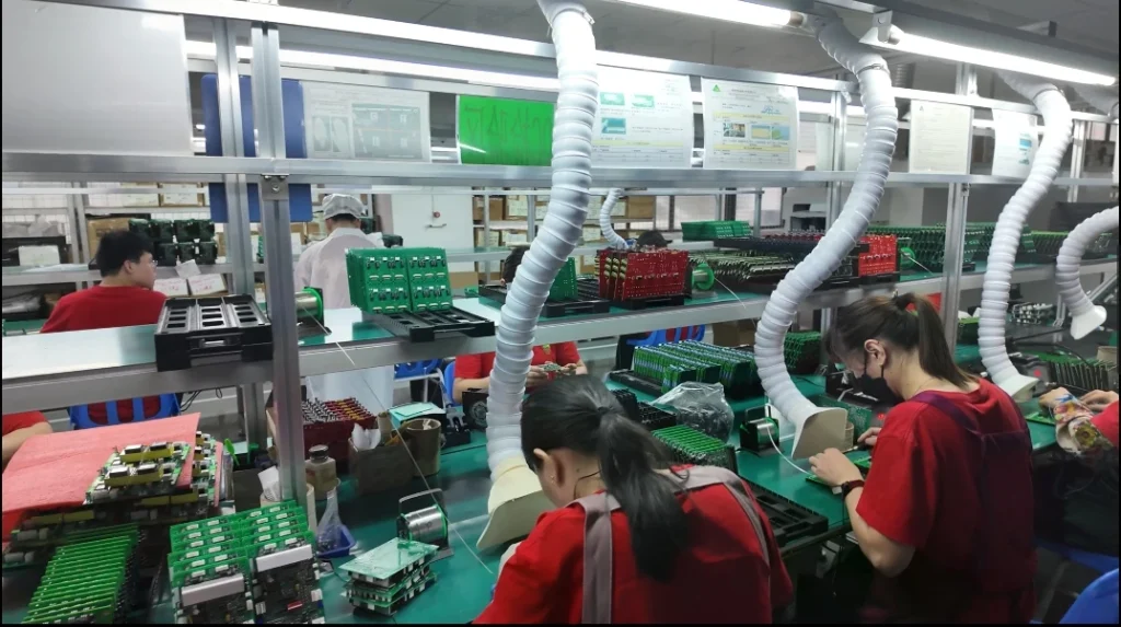
After power-up succeeds, systematic functional testing validates that your design meets specifications.
Basic electrical validation:
- Supply current measurement: Measure total current at nominal voltage. Compare to your pre-design calculations. If the measured current is 50% higher than expected, something is wrong (likely an unintended solder bridge or component failure).
- Rail stability: Measure supply rail ripple and noise using an oscilloscope. Expect <50mV peak-to-peak for 3.3V rails. Larger noise indicates inadequate decoupling or power supply design issues.
- Signal integrity checks (if your design includes high-speed signals):
- Clock frequency verification using an oscilloscope
- Signal edge rates (rise time/fall time)
- No ringing or reflections on critical traces
- Differential pair balance (if you have differential signals like USB or Ethernet)
Functional tests specific to your application:
- Sensor readings: If your design includes sensors, do readings make sense? (Temperature sensor reads 25°C when at room temperature, accelerometer reads 1G on Z-axis, etc.)
- Communication interfaces: USB enumeration, Bluetooth pairing, Ethernet link negotiation—verify every interface works.
- Core algorithm: If your design includes a microcontroller running an algorithm, does the algorithm execute correctly? Does output match expected behavior?
- Edge cases and limits: Test your design at the boundary conditions you specified (minimum/maximum voltage, temperature range if you can test it, maximum load).
Test Documentation and Failure Analysis
For every prototype, maintain a test log:
- Board identifier: Serial number or unique marking so you can track which specific board showed which failures.
- Test date and tester name: Accountability and reproducibility.
- Supply voltage / current readings: Recorded values from your first power-up and steady-state operation.
- Functional test results: Pass/fail for each test, with expected vs. actual values if tests fail.
- Failure root cause (if applicable): “Cold solder joint on R47,” “C15 orientation reversed,” “UART traces have signal integrity issue,” etc.
This log becomes your design history and informs your next revision cycle.

Common Mistakes at This Stage
- No controlled power-up procedure: Connecting full voltage immediately, destroying multiple boards and making diagnosis impossible.
- Inadequate functional test procedures: Testing only “does it power on?” without testing the actual functionality you’re designing for.
- No documentation of test results: Later, you can’t remember whether prototype #2 worked or not.
- Assuming solder joint quality is acceptable without visual inspection: A board might power on but have fragile cold solder joints that fail under thermal cycling or vibration.
IWDF Solutions Tips
We perform first-article inspection on all prototype assemblies and provide you with an FAI report, including photographs of solder joints and component placement. We execute basic functional testing according to your test specification and provide you with supply voltage, current, and basic signal measurements. We can also provide guidance on test procedures—helping you define what “working” means for your specific design. If failures occur during our initial testing, we’ll diagnose root causes (solder issues, component orientation, design flaws) and work with you to determine whether a revision is needed or whether the issue is specific to one board.
Step 7: Iterate, Document and Prepare for Pilot Production
Managing Prototype Revisions Systematically
Your prototype almost certainly won’t be perfect. Design refinements, component substitutions, or layout optimizations will drive one or more revisions. Managing this iteration process determines whether you move to production smoothly or get stuck in endless revision cycles.
Revision nomenclature:
- RevA: Your first assembly (whether it works or not)
- RevB: First planned revision incorporating issues discovered in RevA
- RevC: Further refinements based on RevB feedback
- And so on
Each revision should address specific, documented issues, not be a “kitchen sink” update, including multiple unrelated changes. Keep revisions focused.
Design Change Log: Your Development Record
Maintain a structured change log documenting:
- Revision number (A, B, C)
- Design change: What was changed and why (e.g., “R47: changed from 10kΩ to 12kΩ to reduce noise on analog rail”)
- Justification: Why was this change necessary? (Root cause if addressing a failure, or design improvement if optimizing)
- Risk assessment: What could this change break? (This forces you to think through dependencies)
- Verification method: How will you verify that this change fixed the issue or didn’t break anything?
This log prevents you from forgetting why specific changes were made. Months later, when someone asks, “Why is R47 12kΩ instead of 10kΩ?” you have a clear answer.
Common Iteration Cycles
Typical first revision (RevA → RevB) addresses:
- Power supply noise: If RevA had excessive ripple on supply rails, you might add more bypass capacitors, increase trace width to power planes, or use a different voltage regulator.
- Signal integrity issues: If RevA had noise on high-speed signals, you might add series resistors (termination), shorten trace lengths, or improve ground plane connections.
- Component substitutions: If a component in RevA had availability issues or was prohibitively expensive, you qualify an alternative and update the design.
- Physical layout improvements: If RevA had accessibility issues (hard to probe, hard to service, tight component spacing), you adjust the layout in RevB.
Typical second revision (RevB → RevC) addresses:
- Functional refinements: Adding new features or modifying algorithms based on RevA testing experience.
- Performance optimization: Design-for-cost improvements, power consumption reduction, or thermal optimization.
- Production preparation: Transitioning from prototype-friendly design decisions to production-optimized decisions. For example, RevA might use hand-soldered connectors; RevB/C standardize on assembly-line-compatible components.
Preparing for Pilot Production: The Design Freeze Milestone
At some point, you transition from “prototype iteration” to “production design.” This transition is critical and often mismanaged. Prototype design is opportunistic (change anything for performance or functionality); production design is conservative (change only when necessary).
Design freeze checklist:
- Prototype functionally validated: RevA/B/C has been tested and proven to work reliably. You understand all failure modes and have confirmed fixes.
- BOM rationalized: Every component has been sourced, costs have been negotiated to pilot-production volumes, and alternatives are qualified.
- Supply chain confirmed: 90%+ of your BOM components are available with <8 week lead time at your pilot volume.
- DFM/DFT confirmed: Your latest revision has been reviewed for manufacturability at 500+ unit volumes (pilot scale) and 5,000+ units (early production scale).
- Test procedures documented: Clear, repeatable procedures for verifying the functionality of every pilot batch.
- Documentation complete: Design files, schematics, PCB layouts, assembly drawings, test procedures—all at the same revision level, all archived.
Scalability in Your Prototype Design Decisions
A common mistake is over-optimizing a prototype for cost, then discovering at pilot production that the chosen approach doesn’t scale. You can’t manufacture 5,000 units of a design meant for hand-assembly.
Design for scalability means:
- Using manufacturer-standard components: Custom components or hard-to-source items cause delays at scale.
- Designing for automated assembly: Even at prototype volumes, use components compatible with pick-and-place assembly, not hand-soldering shortcuts.
- Planning for test at scale: The test procedures you used for 1-10 prototypes need to scale to testing 500+ units efficiently.
- Documenting for manufacturing: Your design notes need enough detail that a manufacturing engineer can understand your decisions without calling you.
From your very first prototype, think about how you’ll manufacture 5,000 units. This doesn’t mean building 5,000 in your RevA prototype; it means making design decisions that will scale when the time comes.
Common Mistakes at This Stage
- Endless iteration without decision criteria: Continuously refining without deciding “this is good enough for pilot production.”
- Changing too many things between revisions: Making multiple design changes simultaneously makes it impossible to determine which change fixed which issue.
- Prototype design decisions that don’t scale: Using hand-soldering techniques, custom components, or assembly processes that can’t handle 500+ unit volumes.
- Inadequate design documentation: When it’s time to transition to pilot production, team members have forgotten why specific design decisions were made.
IWDF Solutions Tips
As you transition from prototype toward pilot production, we help you plan the production supply chain, negotiate pilot-volume pricing on your BOM, and identify any design-for-cost opportunities that don’t compromise performance. Our experience scaling designs from 10 units to 50,000+ units means we can spot scalability issues early. We work with you to ensure that your prototype design is genuinely production-ready, not just “functional at small scale.” For pilot production runs, we provide volume discounts on fabrication and assembly, leverage our supplier relationships to reduce lead times, and ensure that pilot production uses identical processes and suppliers to what you’ll use at higher volumes. This continuity means you’ll catch production issues at pilot scale (500-2,000 units) rather than discovering them at 50,000 units when it’s too late and too expensive to change.
When to Work with a One-Stop PCB & PCBA Partner Like IWDF Solutions
Hardware development is complex enough without managing multiple vendors in parallel. From initial requirements clarification through prototype assembly and production ramp-up, IWDF Solutions provides end-to-end support that simplifies your workflow and reduces risk.
A one-stop partner handles:
- Requirements review and design consultation
- Schematic and layout guidance
- DFM/DFT analysis and optimization
- Component sourcing and BOM review
- First-article inspection and functional testing
- Transparent communication across time zones
- Smooth transition from prototype to pilot production
This vertical integration means you have a single point of accountability, simplified communication, and consistent quality standards throughout your development cycle.
Get Your PCBA Prototype Quote in 24 Hours
If you’re a hardware startup or first-time founder ready to build your prototype, IWDF Solutions provides end-to-end PCBA support designed specifically for your needs. We understand the constraints of early-stage hardware development: tight budgets, aggressive timelines, and the need for technical guidance at every stage.
To get started:
- Gather your design files: Schematic, PCB layout, and BOM (even draft versions are fine).
- Clarify your prototype scope: Functional MVP, performance validation, or production-ready?
- Contact us with your specifications: Email your files to our engineering team or complete our online inquiry form.
- Receive your 24-hour quote: We’ll analyze your design, identify any DFM concerns, and provide a transparent quote including component sourcing, fabrication, assembly, and basic testing.
Many early-stage hardware teams are surprised by how affordable professional PCBA services are for prototype quantities. Our goal is to eliminate design uncertainty, accelerate your time to working hardware, and set you up for smooth scaling to production volumes.
Contact IWDF Solutions today to discuss your PCBA prototype requirements. We’ll review your design, identify opportunities, and confirm that your prototype is production-grade from day one.
Conclusion
Building your first PCBA prototype is a structured, manageable process when you follow a clear checklist. From clarifying requirements through design, validation, assembly, and iteration, each step builds on the previous one. Skip steps and you’ll discover problems late; rush through and you’ll waste time and money on preventable mistakes.
This 7-step checklist is your roadmap. Use it to guide your team through prototype development, communicate clearly with your manufacturing partner, and significantly increase your odds of prototype success.
Your first working prototype validates your product vision and positions your startup for accelerated production ramp-up. Make it count.

