
Your project’s design needs more than a basic board. Over-specifying layers wastes budget. Under-specifying causes EMI failures and routing problems that kill your launch timeline.
A multilayer PCB board is a printed circuit board with three or more copper layers, bonded together with insulating materials under heat and pressure. It handles complex, high-speed electronics in a compact, reliable package. Most commercial designs use 4 to 20 layers, chosen based on signal speed, circuit density, and budget.
Most engineers know they need “more layers” for complex designs. But knowing exactly how many — and what type — is where the real decision-making happens. The wrong choice costs real money. The right choice can cut your board size in half, eliminate interference problems, and reduce your assembly failure rate before production even starts. This guide walks you through every decision, from the basics to advanced selection criteria — written for both engineers evaluating options and procurement teams working with PCB suppliers for the first time.
What Exactly Makes a PCB “Multilayer”?
Single-layer boards run out of routing space fast. When a design gets complex, traces start crossing each other — and there is nowhere left to go.
A multilayer PCB board is any printed circuit board with three or more copper layers. Those layers are stacked in a precise sequence, separated by insulating material, and bonded together under heat and pressure into one solid board. The most common configurations start at four layers and go up to 60 or more.
What Is Actually Inside a Multilayer PCB Board?
Every multilayer PCB board is built from the same core elements:
- Core: A rigid, fully cured laminate (usually FR4) with copper foil on both sides. The core is the structural backbone of the board.
- Prepreg: Sheets of fiberglass fabric soaked in partially cured epoxy resin. During lamination, heat and pressure melt the resin and bond all layers into one solid structure.
- Copper layers: Each layer carries etched traces, pads, or solid copper planes — for signals, power distribution, or ground reference.
- Solder mask: A protective coating over the outer copper. It prevents solder bridges during assembly and protects copper from oxidation.
- Silkscreen: Printed markings that identify components, polarity direction, and test points.
- Surface finish: Applied to exposed pads to protect them and ensure reliable soldering. Common options include HASL, ENIG, OSP, and Immersion Silver.
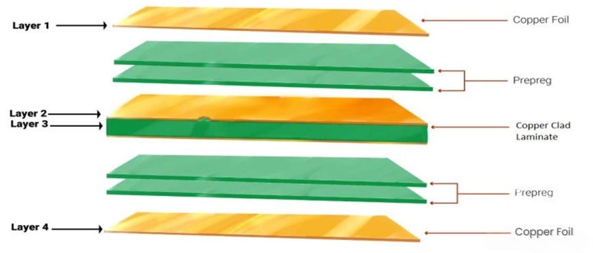
One thing worth understanding clearly: the number of layers in the name refers only to the copper layers — not the total number of physical sheets inside the board. A 4-layer board contains two copper cores, three prepreg sheets, and two outer copper foils. The copper layer count is what defines it as a 4-layer multilayer PCB board.

Why Does the Multilayer Structure Matter for Your Design?
A 2-layer board with the same components as a 4-layer board will often fail electrical tests. The structure is not just about routing space — it changes how the board performs electrically.
The key difference is the dedicated ground plane and power plane that sit in the middle of a multilayer PCB board. These planes do three critical things: they provide a clean, low-impedance return path for every signal on the board, they stabilize the power supply across the entire surface, and they contain electromagnetic fields rather than letting them radiate outward.
How does the Multilayer Structure Change Electrical Performance?
When a signal trace runs over a solid ground plane, the electromagnetic field that the trace produces couples tightly to that plane below it. This is what makes controlled impedance possible. Without a reference plane, the impedance of a trace changes unpredictably depending on what happens to be nearby — other traces, vias, gaps in copper. High-speed signals cannot tolerate that kind of unpredictability.
EMI is the other major issue. A 2-layer board radiates electromagnetic energy because return currents have to find long, indirect paths back to their source. On a multilayer PCB board, return current flows directly beneath each signal trace in the ground plane — the shortest possible path. That tight coupling dramatically reduces the loop area and, with it, the radiated emissions.
Here is how a multilayer PCB board compares to simpler alternatives across the factors that matter most in real designs:
| Feature | Single-Layer PCB | Double-Layer PCB | Multilayer PCB Board |
|---|---|---|---|
| Copper Layers | 1 | 2 | 3 to 60+ |
| Routing Space | Very limited | Moderate | High |
| Signal Integrity | Poor at high speed | Fair | Excellent |
| EMI Control | Poor | Fair | Superior |
| Impedance Control | Not feasible | Difficult | Achievable |
| Board Size for Same Circuit | Large | Medium | Compact |
| Typical Cost | Lowest | Low–Medium | Medium–High |
| Best For | LED lighting, calculators | Power supplies, HVAC | Smartphones, servers, medical |
The jump from a double-sided board to a multilayer PCB board is not just about adding layers. It is about gaining the reference planes that make high-speed PCB design work in the first place. For any design running above 100 MHz, or carrying serial interfaces like USB, Ethernet, or PCIe, a multilayer structure is not optional — it is the baseline requirement.
What Are the Main Types of Multilayer PCB Boards?
Not all multilayer PCB boards are the same. Using the wrong type for your application is a common — and costly — mistake.
Six main types exist. They differ in material, layer count, mechanical properties, and cost. Choosing the right one from the start saves significant time and money later.
FR4 Standard Multilayer PCB Board
This is the most widely used type globally. FR4 is a fiberglass-epoxy laminate that balances cost, mechanical strength, and electrical performance well.
- Layers: 4 to 64
- Tg (Glass Transition Temperature): 130°C standard; 170–180°C for high-Tg variants
- Best for: MCU-based products, IoT devices, consumer electronics, industrial controls
If your design does not involve RF signals above 1–2 GHz or extreme thermal environments, FR4 should be your first choice. It is cost-effective and supported by virtually every PCB manufacturer worldwide.
HDI Multilayer PCB Board
HDI stands for High-Density Interconnect. This type uses laser-drilled microvias (tiny holes, typically ≤0.15 mm) and very fine copper traces to pack more circuitry into a smaller area.
- Layers: 4 to 64
- Key features: Microvias, blind/buried vias, via-in-pad, fine trace/space (≤3 mil)
- Best for: Smartphones, wearables, RF modules, fine-pitch BGA packages
HDI adds manufacturing complexity and cost. But if your design includes 0.4–0.8 mm pitch BGA components, it is often the only practical routing solution.

Flexible Multilayer PCB Board
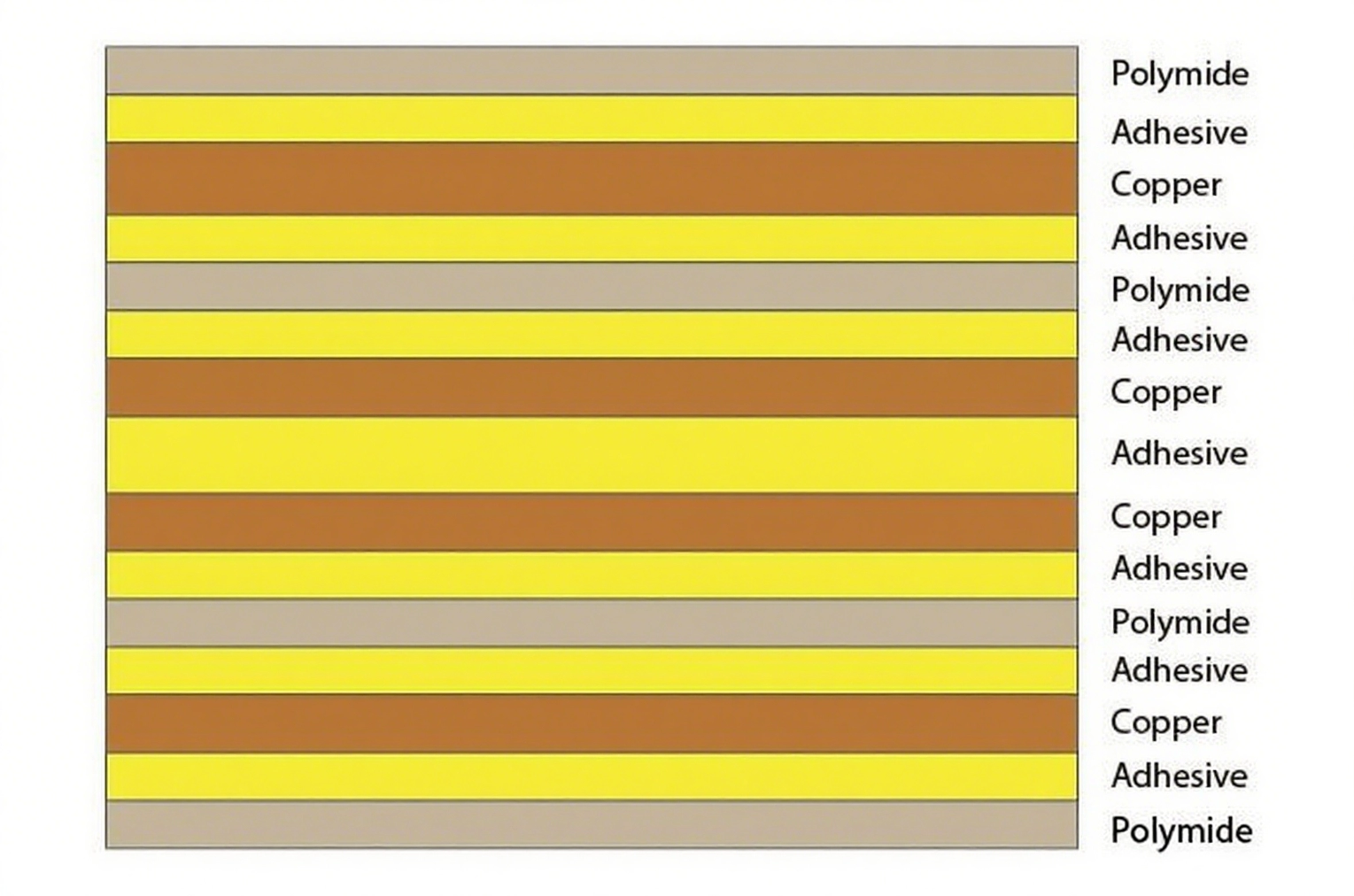
Flexible PCBs use polyimide (a heat-resistant plastic film) instead of rigid FR4. They can bend, fold, and flex repeatedly without cracking or breaking.
- Layers: 2 to 8
- Material: Polyimide (Kapton)
- Best for: Wearables, foldable devices, medical implants, camera modules
The main trade-off is layer count. Flexible boards cannot achieve the same layer depth as rigid boards due to mechanical constraints.
Rigid-Flex Multilayer PCB Board
This type combines rigid FR4 sections (where components mount) with flexible polyimide sections (for 3D interconnection). The rigid areas hold parts. The flex sections connect them without cables or connectors.
- Layers: 2 to 24
- Best for: Aerospace, medical devices, phones with folding mechanisms, military equipment
Rigid-flex eliminates connectors and cable assemblies between separate boards. That reduces weight, assembly steps, and connection failure points — which is precisely why aerospace and medical engineers prefer it despite the higher cost.

High-Frequency Multilayer PCB Board
When signals operate in the gigahertz range, FR4 absorbs too much energy as heat. High-frequency boards use specialty materials with a low dielectric constant (Dk) and low dissipation factor (Df).
- Layers: 4 to 24
- Materials: Rogers, Taconic, PTFE, or hybrid FR4/Rogers stackups
- Best for: 5G base stations, radar systems, satellite links, RF/microwave modules
Rogers laminates cost 5–10× more than standard FR4. For cost-sensitive projects, hybrid stackups — Rogers only on the critical RF layers, FR4 everywhere else — deliver the required electrical performance at a much lower material cost.
Metal-Core Multilayer PCB Board (MCPCB)
These boards use an aluminum or copper base as the substrate instead of fiberglass. The metal base conducts heat away from components far more efficiently than any epoxy laminate.
- Layers: Typically 2 to 4
- Best for: High-power LED lighting, power converters, motor drives, automotive power electronics

Multilayer PCB Board Type Comparison
| Type | Layer Range | Base Material | Primary Use Case | Relative Cost |
|---|---|---|---|---|
| FR4 Standard | 4–64 | FR4 / High-Tg FR4 | General electronics, computing | $ |
| HDI | 4–64 | FR4 + laser drilling | Mobile, wearables, fine-pitch | $$ |
| Flexible | 2–8 | Polyimide | Bending/folding applications | $$–$$$ |
| Rigid-Flex | 2–24 | FR4 + Polyimide | Aerospace, medical, military | $$$ |
| High-Frequency | 4–24 | Rogers / PTFE / Hybrid | RF, 5G, radar | $$$–$$$$ |
| Metal-Core | 2–4 | Aluminum / Copper | High-power thermal management | $$ |
How Many Layers Does Your Project Actually Need?
Most engineers either under-specify and end up with routing problems and EMI failures, or over-specify and pay for layers they do not need. Both mistakes are avoidable.
The layer count controls routing freedom, signal quality, power delivery performance, and a large share of the manufacturing cost. Getting this number right early — before layout starts — prevents expensive redesigns later.
Layer-by-Layer Breakdown
4-Layer Multilayer PCB Board
The 4-layer board is the most common multilayer PCB format in production today.
| Layer | Function |
|---|---|
| Layer 1 (Top) | Signal routing + component placement |
| Layer 2 | Solid ground plane (GND) |
| Layer 3 | Power plane (VCC) |
| Layer 4 (Bottom) | Signal routing + component placement |
The dedicated ground and power planes create a clean return path for signals and built-in distributed capacitance that improves power delivery. This alone solves most EMI problems that plague 2-layer designs.
Use it when: The design has a microcontroller, standard peripherals (SPI, I2C, UART), and operates below 100 MHz.

6-Layer Multilayer PCB Board
A 6-layer board adds one internal signal layer and a second ground plane. This matters when multiple high-speed buses run in parallel, because they need isolation between them to avoid crosstalk.
Use it when: The design involves Ethernet, multiple independent voltage rails, mid-range FPGAs, or automotive ECUs.
8-Layer Multilayer PCB Board
| Layer | Function |
|---|---|
| Layer 1 | Top signal + components |
| Layer 2 | Ground plane |
| Layer 3 | High-speed signal routing |
| Layer 4 | Power plane |
| Layer 5 | Ground plane |
| Layer 6 | Signal routing |
| Layer 7 | Ground plane |
| Layer 8 | Bottom signal + components |
The 8-layer structure gives every signal layer an adjacent reference plane. That is the single most important principle in high-speed layout — it controls impedance and keeps electromagnetic fields contained.
Use it when: The design includes DDR3/DDR4 memory, USB 3.x, PCIe, MIPI CSI/DSI, or Gigabit Ethernet.

10–12 Layers and Beyond
Layer counts of 10 to 12 are standard for complex FPGAs, network switches, and multi-interface processor boards. Above 12 layers, the territory shifts to server motherboards, telecom backplanes, and defense systems.
Quick-Reference Layer Selection Table
| Design Type | Recommended Layers | Typical Frequency | Example Products |
|---|---|---|---|
| Basic sensors, LED control | 2 | < 10 MHz | Lighting, simple sensors |
| MCU + basic peripherals | 4 | 10–100 MHz | IoT devices, USB gadgets |
| MCU + RF or Ethernet | 6 | 100–500 MHz | Wi-Fi routers, automotive ECU |
| Processor + DDR + USB 3.x | 8 | 500 MHz–1 GHz | SBCs, compute modules, cameras |
| Complex FPGA / SoC | 10–12 | 1–5 GHz | Networking switches, medical imaging |
| Server / backplane / HPC | 16–40+ | 5+ GHz | Data centers, defense, telecom |
One rule that should never be compromised: every signal layer needs an adjacent reference plane. If you cannot satisfy that constraint with your current layer count, add more layers. Do not skip the reference plane to save cost — it will cause failures that cost far more to fix.
How Do You Choose the Right Multilayer PCB Board for Your Project?
Most board selection mistakes happen in the first hour of design. Choosing the wrong configuration costs money, time, and — in B2B settings — client trust.
The right approach is a five-step decision process. Each step narrows the options. Together, they lead to a specification that performs as required without wasting budget.
Step 1: Identify Your Fastest Signals
Signal frequency determines the minimum viable stackup.
- Below 100 MHz: A 4-layer board with a dedicated ground plane is almost always sufficient.
- 100 MHz to 500 MHz: You likely need 6 layers with a controlled impedance stackup.
- Above 500 MHz with serial interfaces: 8+ layers, with high-speed signal layers sandwiched between reference planes.
If your design includes DDR memory, USB 3.x, PCIe, or MIPI interfaces, treat each one as a high-speed net — even if the main processor clock appears low. These interfaces carry energy at frequencies that demand impedance control. Target values are typically 50 Ω single-ended and 90–100 Ω differential.
Step 2: Assess Component Density and Board Area
High component density with fine-pitch packages (0.4–0.8 mm pitch BGAs) often forces the layer count upward. Through-hole vias cannot fan out signals from under a dense BGA without laser-drilled microvias and an HDI build-up process.
If board size is constrained by the product enclosure, increasing layers is the only way to route all signals without violating design rules.
Step 3: Check Environmental Requirements
- Operating temperature above 150°C → High-Tg FR4 or polyimide
- Repeated bending or flex cycles → Flexible or rigid-flex multilayer PCB board
- High vibration or shock exposure → IPC Class 3 specifications with stricter testing
- RF operation above 3 GHz → FR4 losses are too high; use Rogers or a hybrid stackup
Step 4: Confirm Applicable Industry Standards
IPC Class 2 covers most commercial electronics. IPC Class 3 applies to high-reliability applications — medical implants, aerospace avionics, military systems. Class 3 boards require tighter tolerances, more rigorous inspection, and additional testing. This directly affects your choice of manufacturer and your unit price.
Step 5: Align Layer Count with Budget and Production Volume
Every additional layer pair adds cost. Here are the approximate impacts for common design decisions:
| Decision | Approximate Cost Impact |
|---|---|
| 4-layer → 6-layer | +40–60% board cost |
| 6-layer → 8-layer | +30–35% board cost |
| FR4 → Rogers material (full board) | +500–1000% material cost |
| Standard vias → blind/buried vias | +20–40% process cost |
| IPC Class 2 → IPC Class 3 | +15–30% inspection and testing cost |
| Prototype quantity → 1,000+ units | −40–60% per-unit cost |
The most common avoidable cost mistake: specifying Rogers material for an entire multilayer PCB board when only two or three layers actually carry RF signals. A hybrid stackup — Rogers only on the RF-critical layers, standard FR4 on everything else — meets the electrical requirement at a fraction of the full-Rogers cost.

What Happens Inside a Multilayer PCB Factory?
Most buyers treat manufacturing as a black box. Understanding the process helps you write better specifications, catch design issues early, and have more productive conversations with suppliers.
Here is what actually happens after your Gerber files arrive at a multilayer PCB factory:
The Complete Manufacturing Process
Step 1 — Material cutting: Core laminates and prepreg sheets are cut to panel size. Material specs (FR4 grade, copper weight, dielectric thickness) are verified against the order before anything else happens.
Step 2 — Inner layer imaging: Each inner copper layer is coated with photoresist, then exposed to UV light through a photomask. The unexposed resist is developed away, and the unprotected copper is chemically etched — leaving only the designed traces, pads, and planes.
Step 3 — Inner layer AOI: Every inner layer is scanned by automated optical inspection before lamination. Opens, shorts, and trace width violations are caught here. This is the only point in the process where inner-layer defects can be identified and fixed. After lamination, nothing can be repaired.
Step 4 — Oxide treatment: Inner layer copper surfaces are chemically roughened at the microscopic level. This creates a mechanical key that improves adhesion between the copper and the prepreg resin during lamination.
Step 5 — Stackup and lamination: All layers — cores, prepreg sheets, and outer copper foils — are aligned precisely using registration pins or optical alignment systems, then stacked in the correct sequence. The stack goes into a hydraulic press at 175–190°C and 200–400 PSI. The prepreg resin melts, flows, and cures, bonding everything into one solid multilayer PCB board. Misalignment at this stage ruins the entire panel.
Step 6 — Mechanical drilling: CNC-controlled machines drill all through-holes and mounting holes. Minimum mechanical hole size is typically 0.2–0.3 mm (8–12 mil).
Step 7 — Laser drilling (HDI only): For blind microvias in HDI multilayer PCB boards, CO₂ or UV lasers drill holes as small as 0.05 mm — dimensions impossible to achieve with mechanical drill bits.
Step 8 — Electroless copper and electroplating: The drilled hole walls (exposed fiberglass and resin) are non-conductive. An electroless chemical process deposits a thin copper seed layer on the hole walls. Electroplating then builds this up to the specified copper thickness, creating the via connections between layers.
Step 9 — Outer layer imaging and etching: The same photolithographic process used for inner layers is applied to the outer copper foils to create the top and bottom circuit patterns.
Step 10 — Solder mask application: A liquid photoimageable solder mask (most commonly green, but available in multiple colors) is applied across the entire outer surface, then exposed and developed to open only the solder pads.
Step 11 — Surface finish: Exposed copper pads receive their specified finish. The most common options and their trade-offs:
| Surface Finish | Shelf Life | Flatness | Cost | Best Application |
|---|---|---|---|---|
| HASL (Lead-Free) | 12+ months | Moderate | Low | General SMT, through-hole |
| ENIG (Gold) | 12+ months | Excellent | High | Fine-pitch BGA, wire bonding |
| OSP | 6 months | Excellent | Lowest | High-volume SMT lines |
| Immersion Silver | 6–12 months | Excellent | Medium | High-frequency, membrane switch |
| Immersion Tin | 6 months | Excellent | Medium | Press-fit connectors |
Step 12 — Silkscreen: Component references, polarity markers, and other identifiers are printed onto the solder mask surface.
Step 13 — Profiling and depanelization: Individual boards are cut from the production panel by CNC routing, V-scoring, or laser cutting.
Step 14 — Electrical testing: Every board is tested 100% for continuity (no open circuits) and isolation (no short circuits). Prototypes typically use flying probe testing. Volume production uses custom bed-of-nails fixtures for faster throughput.
The step most clients underestimate is the inner-layer AOI at Step 3. It is the gatekeeper of the entire process. A manufacturer who skips it to cut time is making a gamble with your product quality.
What Drives the Cost of a Multilayer PCB Board — and How Can You Reduce It?
Price quotes for the same multilayer PCB board design can vary by 200–300% between suppliers. The difference is not always quality — it is often material choices, production volume, and avoidable design decisions.
Understanding the cost drivers tells you where to optimize and where cutting corners creates risk.
Primary Cost Drivers
Layer count is the single biggest cost variable:
| Layer Count | Approximate Cost vs. 2-Layer Baseline |
|---|---|
| 2 layers | 1× (baseline) |
| 4 layers | ~2× |
| 6 layers | ~3–3.5× |
| 8 layers | ~4–5× |
| 10–12 layers | ~6–8× |
| 16+ layers | 10× and above |
Beyond layer count, these factors add significant cost:
- Material selection: Rogers laminates cost 5–10× more than standard FR4. High-Tg FR4 adds only a modest 10–20% premium over standard FR4.
- HDI features: Blind and buried vias, microvias, and sequential lamination add 20–40% to process cost.
- Copper weight: Heavier copper (2 oz, 3 oz) for high-current power stages raises both material and etching cost.
- Surface finish: ENIG costs more than HASL but is necessary for fine-pitch BGA components. Using ENIG on boards with only through-hole connectors is wasteful.
- Board size and panel utilization: Larger boards and irregular shapes reduce the number of boards per production panel, raising per-unit cost directly.
- IPC class: IPC Class 3 testing and inspection requirements add approximately 15–30% over Class 2.
- Production volume: Setup costs are fixed. Spreading them over more units is the fastest way to reduce per-unit price.
Cost Reduction Strategies That Actually Work
Use the minimum layer count that meets your requirements. Every unnecessary layer pair adds real cost with no electrical benefit.
Use a hybrid stackup for RF designs. Rogers only on the signal-critical layers, FR4 everywhere else. This can cut material cost by 70–80% compared to a full-Rogers board while meeting the same electrical performance spec.
Standardize stackups across product families. When your manufacturer already runs a specific stackup in production, you avoid custom engineering setup fees and reduce lead time.
Select surface finish by function. ENIG where fine-pitch BGAs require it. HASL or OSP everywhere else on the same board — if your manufacturer supports selective surface finishes.
Run a DFM (Design for Manufacturability) review before finalizing the design. A 30-minute review can catch trace width violations, annular ring issues, drill aspect ratio problems, and copper-to-edge clearance violations that would otherwise cause yield loss or trigger a costly board revision.
Plan volume production early. If the total annual demand justifies it, ordering larger batches reduces per-unit cost significantly. Even going from a 50-piece prototype order to a 500-piece initial production run can cut unit price by 30–40%.
Frequently Asked Questions About Multilayer PCB Boards
Q1: What is the minimum number of layers in a multilayer PCB board?
Three layers are the technical minimum. In practice, four layers is the standard starting point because it allows a symmetric stackup — which prevents board warpage during lamination and reflow. Even-numbered layer counts are the norm in production.
Q2: Why do multilayer PCB boards use even numbers of layers?
Even layer counts produce a symmetric stackup structure. A symmetric structure distributes thermal stress evenly during lamination and soldering. Asymmetric stackups flex under heat, which causes warping. Warped boards create assembly problems and long-term reliability issues in the field.
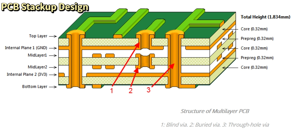
Q3: What is the difference between a blind via and a buried via in a multilayer PCB?
A blind via connects an outer layer to one or more inner layers. It is visible from one surface of the board. A buried via connects two inner layers only — it is completely hidden inside the board and invisible from either surface. Both are used in HDI multilayer PCB boards to maximize routing density without consuming outer-layer real estate.
Q4: Can a defect in an inner layer of a multilayer PCB board be repaired?
No. Once a multilayer PCB board is laminated, the inner layers are permanently sealed inside. Any inner-layer defect found after lamination makes the panel scrap. This is why automated optical inspection of all inner layers before lamination is a non-negotiable quality step in any serious manufacturing operation.
Q5: How long does it take to manufacture a multilayer PCB board?
Standard lead times: 4-layer boards take 5–7 working days; 6–8 layer boards take 7–10 working days; 10+ layer boards take 10–15 working days or longer. Quick-turn (expedited) service can reduce 4-layer prototype lead times to 24–72 hours, depending on the manufacturer’s capacity.
Q6: What files does a manufacturer need to produce a multilayer PCB board?
You need complete Gerber files (or ODB++ / IPC-2581 format) for all layers — including copper, solder mask, silkscreen, and drill files. You also need a stackup drawing that specifies layer sequence, material type, copper weights, finished board thickness, and any controlled impedance requirements. A fabrication drawing covering board outline, dimensions, tolerances, surface finish, and special features (edge plating, half-holes, countersinks) completes the package.
Q7: What is PCB reverse engineering, and when does it apply to multilayer boards?
PCB reverse engineering is the process of extracting design files — Gerber files, schematics, and bill of materials — from an existing physical board. Engineers use it when original design files are lost, when a legacy product needs to be re-manufactured, or when an existing design must be modified without the source files. It applies to multilayer PCB boards including designs with up to 32+ layers and complex via structures like blind and buried vias.
Q8: How do I decide between FR4 and Rogers material for a multilayer PCB board?
If your design operates below 1–2 GHz, FR4 is almost always sufficient and far more cost-effective. Above 2 GHz — especially for 5G, radar, or satellite communication hardware — FR4 dielectric losses become unacceptable, and Rogers or PTFE-based materials are required. For mixed-frequency designs, a hybrid stackup with Rogers on the RF-critical signal layers and standard FR4 on the rest is the most practical and cost-effective solution.
Conclusion
Choosing a multilayer PCB board comes down to one principle: let your electrical requirements lead, and let everything else follow. Start with your fastest signal. Use that to set the minimum layer count. Then align your material, stackup, and surface finish to match — without over-specifying.
Every unnecessary layer, every premium material used where standard FR4 would work, adds cost with no return.
If you need a multilayer PCB board manufactured, designed, or reverse engineered, IWDF Solutions is ready to help. Send us your files and get a detailed quote within 24 hours.
IWDF Solutions is a PCB factory in Shenzhen, China. We provide multilayer PCB board manufacturing, PCB design, PCB reverse engineering, PCB cloning, and PCBA production for clients worldwide. Contact our engineering team to discuss your project.

