

Your board keeps running out of routing space. Signals fail. EMC tests come back negative. These are not random problems — they are signs you are using the wrong PCB structure.
Multi-layer PCBs solve these problems by stacking signal, power, and ground layers into one compact board. They give you more routing freedom, cleaner signals, lower EMI, better power delivery, and a smaller board size — all built into the structure from the start.
If you have already hit the limits of a single or double-sided board, you know the frustration: traces that will not fit, ground pours that do not actually work, and layout compromises that later cause failures during testing. Moving to a multi-layer PCB is not just an upgrade — it is the right tool for the problem you are actually trying to solve. This article walks through 13 real benefits in plain terms, helps you decide which ones matter most for your specific design type, and tells you what to look for when choosing a manufacturing partner.

What Exactly Is a Multi-Layer PCB?
A multi-layer PCB is a printed circuit board with three or more conductive copper layers. Each layer is bonded to the next using insulating material called prepreg. Unlike a 2-layer board — where both surfaces simply carry traces — each layer in a multi-layer PCB has a specific role: signal routing, power distribution, or ground reference.
That defined role per layer is the core difference. A 2-layer board gives you two surfaces to place traces. A multi-layer PCB gives you a structured system where signals, power, and ground each occupy their own dedicated space. This structure is what makes the electrical performance gains possible — not the layer count alone.
A poorly planned 8-layer board can perform worse than a well-planned 4-layer board. The number of layers matters less than how each layer is used.
How Does a Multi-Layer PCB’s Internal Structure Actually Work?
Knowing a board has “more layers” is not enough. Where those layers sit and what each one does determines everything.
The arrangement of layers from top to bottom is called the stack-up. The stack-up controls signal impedance, EMI behavior, power delivery quality, and mechanical stability. Every electrical performance benefit of a multi-layer PCB flows directly from how the stack-up is planned.
What does a typical 4-layer stack-up look like?
For a standard 4-layer multi-layer PCB, the most common arrangement is:
| Layer | Role | What it does |
|---|---|---|
| Layer 1 (Top) | Signal + components | Carries high-priority traces and surface-mounted parts |
| Layer 2 | Ground plane | Provides a solid return path for every signal above it |
| Layer 3 | Power plane | Distributes one or more supply rails across the board |
| Layer 4 (Bottom) | Signal + components | Carries remaining traces and bottom-side parts |
This arrangement places every signal on Layer 1 directly above a solid ground plane on Layer 2. That proximity is what creates controlled impedance and low EMI — two of the most critical benefits in multi-layer PCB design.

How does the stack-up change as layer count increases?
As designs grow more complex, more layers are added in pairs to keep the stack-up symmetric. Symmetry matters because an unbalanced structure warps during the lamination process.
A 6-layer stack adds one more signal layer and one more reference plane compared to a 4-layer board. A common 6-layer arrangement looks like this:
| Layer | Role |
|---|---|
| Layer 1 | Signal (Top) |
| Layer 2 | Ground plane |
| Layer 3 | Signal (internal) |
| Layer 4 | Power plane |
| Layer 5 | Ground plane |
| Layer 6 | Signal (Bottom) |
This gives you one extra internal signal layer with ground planes on both sides — a significant gain for mixed-signal and mid-complexity high-speed designs.
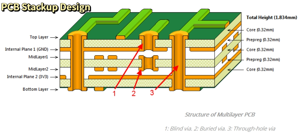
For more demanding projects, an 8-layer stack follows the same principle with one more signal-and-plane pair added symmetrically:
| Layer | Role |
|---|---|
| Layer 1 | Signal (Top) |
| Layer 2 | Ground plane |
| Layer 3 | Signal (internal) |
| Layer 4 | Power plane |
| Layer 5 | Ground plane |
| Layer 6 | Signal (internal) |
| Layer 7 | Ground plane |
| Layer 8 | Signal (Bottom) |
Each internal signal layer sits between two reference planes. This is the standard pattern for high-speed digital designs involving DDR memory, PCIe, or FPGA-heavy boards.

Why does the stack-up need to be agreed on before routing?
The stack-up defines the dielectric thickness between each layer and the copper weight on each layer. These two values directly determine the impedance of every signal trace on the board. If you finalize your stack-up after routing, you may discover that your trace widths produce the wrong impedance — and changing them means re-routing the entire board.
The right approach is to agree on the stack-up with your PCB manufacturer before layout begins. They can provide a verified impedance table showing which trace width produces 50 Ω or 100 Ω on each signal layer. This turns a guessing step into a confirmed specification.
What Are the Benefits of Multi-Layer PCBs for Complex Designs?
If you added ferrite beads, shielding cans, and extra capacitors — and the board still fails. That is what happens when you try to fix a structural problem with patches.
Multi-layer PCBs solve the root cause. They bring higher routing capacity, cleaner signal quality, lower noise, stronger power delivery, better thermal control, smaller size, and longer product life — all built into the board structure from the beginning.
1. Higher Component Density Without Expanding Board Size
On a 2-layer board, there are only two surfaces for traces. Once components fill the top and signals crowd the bottom, routing space runs out. The only options are to make the board bigger, add more inter-board connectors, or make painful layout compromises that create noise and timing issues later.
A multi-layer PCB gives you routing channels inside the board. Signals on internal layers connect to surface components through short vias. This approach typically reduces board area by 30–50% for the same circuit function. Dense BGA fanout, multiple power rails, and mixed-signal layouts all become manageable instead of forced.

2. Superior Signal Integrity and Controlled Impedance
High-speed interfaces — USB 3.0, PCIe, DDR4/5, LVDS, HDMI — behave like transmission lines. Their performance depends on impedance, trace geometry, and the reference plane beneath the trace. On a 2-layer board, there is no reliable way to control these factors consistently.
A multi-layer PCB lets you route each high-speed signal directly above a solid ground plane. This gives the trace a predictable reference, a defined impedance (typically 50 Ω single-ended or 100 Ω differential), and a short, clean return path. The result is less signal reflection, less overshoot, and more stable timing. Without controlled impedance, USB links drop frames, DDR memory fails at speed, and HDMI signals show visual artifacts. Controlled impedance is only practical on a multi-layer board.
3. Reduced Electromagnetic Interference (EMI)
A failed EMC test after product completion is one of the most expensive events in electronics development. Each retest session typically costs $5,000–$15,000 and delays a product launch by weeks.
The main cause of EMI is large current loops. When a signal travels outward and its return current must travel a long path back, that loop radiates like an antenna. A solid ground plane under every signal layer removes this problem. Return current follows the path directly under its signal trace, keeping the loop area very small. A 4-layer board with a proper ground plane produces approximately 15 dB less radiated EMI than a 2-layer board running the same circuit. That extra margin is often the difference between passing and failing without hardware changes.

4. Cleaner Crosstalk Control Between Signal Layers
Crosstalk happens when energy from one trace bleeds into a nearby trace. On a 2-layer board, all signals share the same surface. A fast clock edge on one trace injects noise into everything around it, including sensitive analog inputs and RF front-ends.
A multi-layer PCB lets you separate sensitive signals onto different layers with ground planes between them. RF signals go on one layer, digital signals on another, analog signals on a third. The ground plane acts as a vertical shield between them. Critical differential pairs can be routed internally as striplines — fully enclosed by copper planes on both sides — which minimizes both radiated interference and susceptibility to outside noise.
5. Greater Design Flexibility and Routing Freedom
On a 2-layer board, every routing decision is a compromise. You cannot cross two signals without a via chain. You cannot dedicate a full layer to a power rail. You cannot physically separate a noisy switching stage from a sensitive ADC front-end.
A multi-layer PCB gives you freedom in the third dimension. You can dedicate one full layer to a critical power rail, giving every part of the board direct access to a low-impedance supply. You can route high-speed signals on layers closest to ground planes and push lower-speed signals to outer layers. You can keep analog, digital, and RF sections separated both horizontally and vertically. Engineers who regularly design multi-layer boards consistently report shorter layout times and fewer board respins compared to dense 2-layer designs pushed to their limits.
6. Better Power Distribution and Stable Supply Rails
Unstable power rails cause random resets, ADC noise, and communication errors. These bugs are hard to trace because the symptoms appear far from the actual cause.
A solid copper power plane in a multi-layer PCB behaves like a distributed capacitor. It stores charge close to every component simultaneously. When a chip draws a sudden burst of current, the plane delivers it without the voltage dip that a narrow trace would cause. Combined with strategically placed decoupling capacitors, this creates a low-impedance power delivery network (PDN) that stays stable under rapid load changes. For designs with multiple supply rails, you can dedicate one internal layer to each rail, keeping supplies from interfering with each other.
7. Improved Thermal Management
Heat is one of the most common causes of field failures. Multi-layer PCBs address thermal problems in ways that single or double-sided boards simply cannot.
Internal copper planes act as heat spreaders. They move heat horizontally away from a hot component before it builds up in one spot. Thermal via arrays — typically 0.3–0.5 mm drilled holes under an exposed component pad — create a vertical heat path from the top surface down to an internal copper plane. A practical implementation for a power IC dissipating 3–5 W uses an exposed pad footprint, a 3×3 or 4×4 thermal via array, and a large copper pour on the bottom layer acting as a secondary spreader. Without extra internal layers, this kind of thermal structure is not possible.

8. Compact and Lightweight Form Factor
When you replace multiple interconnected single or double-sided boards with one multi-layer PCB, the system gets smaller and lighter. You eliminate inter-board connectors, wire harnesses, and the mechanical structures needed to hold them together.
In aerospace, weight reduction directly lowers fuel cost over the product’s operational life. In portable medical devices, a lighter board means a more comfortable device. In smartphones and wearables, it is why these devices keep getting thinner each generation. HDI multi-layer PCBs — those using microvias and fine-pitch routing — can reduce device size by 30–40% compared to a standard multi-layer design at the same function level.
9. Greater Mechanical Durability and Reliability
A multi-layer PCB is a single laminated unit. The heat-and-pressure bonding process creates a mechanically strong structure that resists vibration, bending, and thermal cycling far better than a loosely connected multi-board assembly.
For automotive under-hood applications, multi-layer boards withstand temperature swings from −40 °C to +125 °C and constant mechanical vibration without delaminating or cracking solder joints. For industrial equipment mounted on machinery, the rigid laminated structure prevents connector loosening. The IPC-6012 standard defines three performance classes for rigid PCBs. Class 3 — used in aerospace and medical devices — requires multi-layer construction with tight lamination controls as a baseline requirement.
10. Faster Signal Speeds and High-Frequency Interface Support
Every major high-speed interface standard introduced in the last decade requires a multi-layer PCB. There is no practical alternative.
| Interface | Minimum speed | What multi-layer PCB enables |
|---|---|---|
| USB 3.x / USB4 | 5–40 Gbps | Controlled impedance differential pairs, solid ground reference |
| PCIe Gen 4 / Gen 5 | 16–32 GT/s | Low-loss stripline routing, minimal via stubs |
| DDR4 / DDR5 | > 3,200 MT/s | Matched-length routing, stable power planes |
| HDMI 2.1 | 48 Gbps | Tight differential pair control, low crosstalk |
| 5G mmWave RF | > 28 GHz | Low-loss materials, precise impedance |
Shorter internal signal paths reduce parasitic inductance and capacitance. This directly lowers signal delay and allows faster, cleaner signal edges. If your product roadmap includes any interface in the table above and you are still on a 2-layer board, you will hit a hard limit at some point. Moving to multi-layer PCB design is risk control, not luxury.
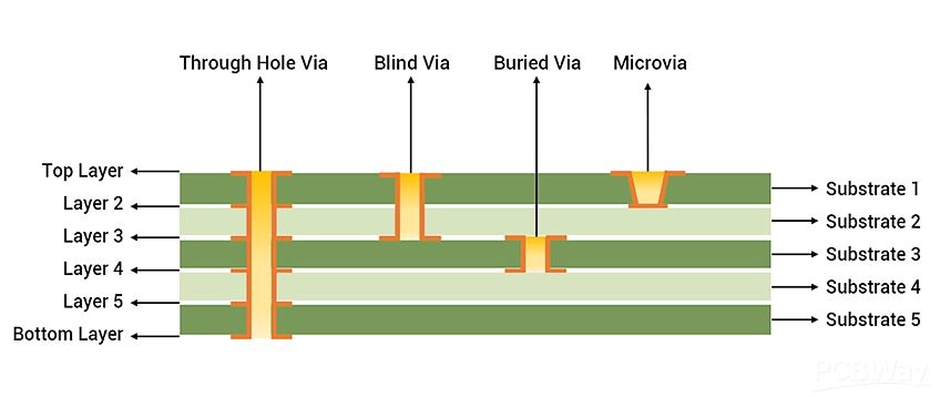
11. Support for HDI Technology — Blind Vias, Buried Vias, and Microvias
This benefit is exclusive to multi-layer PCBs. You cannot have blind or buried vias on a 2-layer board because there are no internal layers to connect to.
Blind vias connect an outer layer to one or more inner layers without passing through the full board. Buried vias connect inner layers only, invisible from both surfaces. Microvias are laser-drilled holes smaller than 0.15 mm, used to fan out fine-pitch BGAs at 0.4 mm pitch or below. These features dramatically increase routing density in a small area. They also reduce via parasitic effects at high frequencies, improving signal integrity for chips with very tight electrical requirements. For modern AI accelerators, smartphone SoCs, and advanced networking silicon, HDI multi-layer PCB design is a necessity, not an option.
12. Long-Term Cost Efficiency Over Single and Double-Layer Alternatives
The upfront cost of a multi-layer PCB is higher than a 2-layer board. That is true. But the right comparison is total project cost, not bare board cost alone.
Consider what a 2-layer design costs when it goes wrong:
- One EMC test failure: $5,000–$15,000 in retesting fees, plus weeks of launch delay
- A layout respin due to routing failure: $3,000–$10,000 in engineering time
- Field failures from unstable power or thermal issues: warranty costs and reputation damage
A multi-layer PCB built correctly from the start often avoids all of these. The added board cost — sometimes as little as $0.50–$2.00 per unit in volume production — is small compared to those downstream risks. Multi-layer PCBs also reduce system cost by replacing multiple boards and connectors with one reliable, fully integrated unit.
13. Consistent Scalability from Prototype to Volume Production
A well-designed multi-layer PCB is inherently more reproducible than a complex 2-layer board pushed to its limits. The fabrication process — automated lamination, precision etching, controlled drilling — produces consistent results at scale.
Impedance targets validated on your prototype carry through to your production run because the stack-up and materials are documented and repeatable. Your signals behave the same way at unit 5 as they do at unit 5,000. This consistency matters directly for certification. If your product requires CE, FCC, UL, or medical device approval, you need to demonstrate that every unit leaving the factory performs the same way. A multi-layer PCB with a documented stack-up specification makes that proof far easier to build.
These 13 benefits do not all carry equal weight for every project. The next step is to identify which ones should actually drive your layer count decision.
Which of These Benefits Matter Most for Your Specific Design?
Every project is different. Spending money on layers you do not need is a waste. Skipping layers you do need is a risk.
Match your design type to the benefits that should drive your layer count decision. Not every benefit requires the same number of layers to achieve. The table below gives you a starting point.
| Design type | Primary challenge | Most critical benefits | Practical layer count |
|---|---|---|---|
| Simple IoT sensor / controller | Routing congestion, board size | Component density, compact form, power stability | 4 layers |
| Wireless device (Wi-Fi, BLE, Zigbee) | RF isolation, antenna performance | EMI reduction, crosstalk control, design flexibility | 4–6 layers |
| High-speed digital (DDR, PCIe, USB3+) | Signal integrity, impedance matching | Controlled impedance, high-frequency support, HDI | 6–8 layers |
| Mixed-signal (analog + digital) | Noise coupling between domains | Signal integrity, crosstalk control, power distribution | 6–8 layers |
| Automotive ECU / ADAS system | Reliability, wide temperature range | Durability, thermal management, EMI reduction | 6–8 layers |
| Medical device | Precision, long service life, compliance | Signal integrity, reliability, scalability | 6–10 layers |
| Telecom / 5G base station | High frequency, low signal loss | Controlled impedance, HDI, low-loss materials | 8–12 layers |
If you are deciding between two layer counts, lean toward the higher one. The cost difference between 4 and 6 layers, or between 6 and 8 layers, is smaller than most engineers expect. The routing margin and signal integrity headroom that extra layers provide is substantial, and it is much cheaper than a board respin later.
How Do These Benefits Apply Across Different Industries?
The same core benefits appear in every industry. What changes is which ones take priority — and how strictly they must be controlled.
In automotive electronics — ADAS cameras, EV battery management, and infotainment systems — durability and thermal performance lead. Boards must withstand temperature swings from −40 °C to +125 °C and constant mechanical vibration across a vehicle’s service life of 10–15 years. Multi-layer PCBs built to IATF 16949 quality standards are the baseline expectation here.
In medical devices — patient monitors, diagnostic imaging systems, and infusion pumps — signal integrity and long-term reliability are non-negotiable. A single noise event or power dropout can affect a reading or, in a critical care setting, patient safety. Multi-layer PCB design gives medical engineers the control needed to meet ISO 13485 and IEC 60601 requirements.
In 5G infrastructure and telecommunications — base stations, high-capacity routers, and optical network units — high-frequency signal integrity is the dominant requirement. Boards here use specialized low-loss materials and 8–16 layers to carry millimeter-wave signals with minimal attenuation.
In consumer electronics and IoT — smartphones, wearables, and smart home hubs — the emphasis falls on size, weight, and unit cost. HDI multi-layer PCBs shrink the board while increasing function density, enabling thinner and lighter products at competitive price points.
In industrial automation and energy systems — motor drives, PLCs, and solar inverters — heavy copper planes handle high currents without voltage drop, and robust lamination survives factory-floor vibration and contamination over years of continuous operation.
How Do You Choose the Right Multi-Layer PCB Design and Manufacturing Partner in China?
Choosing a partner based only on the lowest quote is a risk most B2B buyers regret on a complex project.
The best multi-layer PCB partners in China do more than manufacture. They review your design before production, flag DFM issues, suggest stack-up improvements, and provide documented test data. This engineering involvement at the start of a project prevents costly problems at the end.
When evaluating a Chinese PCB and PCBA supplier, check these specific points:
| Evaluation point | What to ask | Why it matters |
|---|---|---|
| Layer count range | Do they build 4-to-16+ layer boards in-house? | Outsourced production adds risk and delays |
| Via capabilities | Do they offer blind, buried, and laser-drilled vias? | Required for HDI and fine-pitch BGA designs |
| Impedance control | Do they offer TDR (Time Domain Reflectometry) testing? | Verifies that built boards match your designed impedance |
| Quality certifications | ISO 9001? IATF 16949 for automotive? ISO 13485 for medical? | Confirms alignment with your industry standards |
| DFM support | Will they review your files and flag issues before production? | Prevents redesigns and production delays |
| PCBA capability | Do they handle assembly, component sourcing, and testing in-house? | One-stop service removes handoff errors |
| Communication | English-speaking engineers? Consistent response within 24 hours? | Prevents misunderstandings and schedule slippage |
IWDF Solutions, based in Shenzhen, provides a complete one-stop service covering multi-layer PCB design, multi-layer PCB fabrication (4–32+ layers), PCB reverse engineering, and full PCBA production. Our engineering team supports clients from stack-up planning through final functional testing — not just at the manufacturing stage. Every project receives a DFM review, impedance simulation confirmation, and material recommendation before a single board enters production.
For overseas clients, a one-stop partner removes the coordination overhead that comes from splitting PCB fabrication, component sourcing, and assembly across different vendors. One team owns the result. One contact person answers your questions. When something needs to be resolved, it gets resolved faster.
FAQ
What is the minimum layer count that qualifies as a multi-layer PCB?
A multi-layer PCB starts at three layers. In practice, four layers is the most common entry point, because it allows at least one dedicated ground plane and one additional power or signal layer. Three-layer boards exist but are rarely used, because a 4-layer structure provides meaningfully better performance without a proportionally large cost increase.
Is a 4-layer multi-layer PCB significantly more expensive than a 2-layer board?
Yes, but the gap is smaller than most engineers expect. At prototype quantities, a 4-layer board typically costs 2–3× more than a comparable 2-layer board. At volume production, that gap narrows. When you factor in layout time saved, EMC failures avoided, and board respins prevented, the 4-layer option is often the lower total cost over the full project lifecycle.
Can I still use a 2-layer board for a complex design?
You can, but you will hit limits. If your design has only low-speed signals, a single supply rail, and moderate component density, 2 layers may work. As soon as you add USB, Ethernet, DDR memory, or a switching power supply, a 2-layer board becomes a constant source of layout compromises and debugging problems. The question is not whether the parts will fit — it is whether the board can meet your electrical, thermal, and compliance requirements.
What is a PCB stack-up and why does it matter so much?
A stack-up is the specific arrangement of copper layers, dielectric materials, and their thicknesses in a multi-layer PCB. It determines signal impedance, power delivery quality, EMI performance, and mechanical stability. A poorly planned stack-up can produce a board that looks correct in the design tool but fails EMC tests or shows signal integrity problems during testing. Always finalize the stack-up with your manufacturer before routing begins, not after.
Do I need HDI — blind and buried vias — for my multi-layer PCB design?
Only if your component density demands it. HDI is necessary when you use fine-pitch BGAs at 0.4 mm pitch or smaller, and through-hole vias cannot provide enough escape routing without consuming too much board area. For most industrial and mid-complexity consumer designs, standard through-hole vias on a 4–8 layer multi-layer PCB are sufficient. Using HDI when your design does not require it typically increases fabrication cost by 20–50% with no performance benefit.
What certifications should a multi-layer PCB manufacturer hold?
At a minimum: ISO 9001 for general quality management. For automotive projects: IATF 16949. For medical projects: ISO 13485. For market access: UL listing for North America, and RoHS/WEEE compliance for Europe. Do not accept a certificate image alone — ask for the certificate number and verify it on the issuing organization’s official website. Some suppliers display certificates that are expired or were issued to a different entity.
Can IWDF Solutions handle both multi-layer PCB design and manufacturing together?
Yes. IWDF Solutions provides multi-layer PCB design, stack-up planning, PCB reverse engineering, board fabrication (4–48+ layers), component sourcing, PCBA assembly, and functional testing — all under one roof in Shenzhen, China. This integrated one-stop service is built for overseas B2B clients who need a single accountable partner from the first design file to the final shipped assembly.

