

Mobile PCB boards are the nervous system of modern smartphones, enabling seamless communication between processing units, memory, power systems, and connectivity modules. As smartphones continue to evolve toward higher performance, thinner designs, and advanced capabilities—including 5G connectivity and artificial intelligence processing—the demands on PCB technology become increasingly sophisticated.
In this guide, we explore the complete landscape of mobile PCB boards—from fundamental concepts through advanced manufacturing techniques—to provide you with the technical foundation necessary for informed decision-making when sourcing or redesigning mobile PCB solutions.


Mobile Phone PCB Board Types: Understanding the Architecture
Mobile devices employ three primary PCB categories, each with distinct structural properties and manufacturing considerations that influence design choices.
Rigid PCBs: The Foundation of Mobile Architecture
Rigid PCBs form the primary structural and functional backbone of smartphones. Constructed from solid FR-4 (fiberglass-reinforced epoxy) or polyimide materials, these boards provide the mechanical strength required to support high-density component placement while maintaining signal integrity.
Structural Properties:
Rigid PCBs use laminated layers of copper and insulating material bonded together under heat and pressure. A typical mobile device main board might employ 6 to 10 copper layers, depending on circuit complexity. The manufacturing process involves photolithography for precise pattern transfer, etching to remove unwanted copper, drilling for through-holes and vias, and multiple plating processes to ensure reliable interconnections.
Performance Advantages:
The well-established manufacturing processes for rigid PCBs enable cost-effective production at high volumes. Material consistency and standardized manufacturing parameters result in predictable electrical properties, making rigid PCBs ideal for time-critical product launches. Design tools and simulation software for rigid boards are mature and widely available, reducing development risk.
Typical Applications:
Rigid PCBs serve as the main logic boards for processors, power management sections, RF modules, and battery management systems. The central location of the main board provides optimal thermal conditions for the device’s hottest components—the application processor and modem—where heat dissipation capabilities are crucial.

Flexible PCBs: Enabling Mechanical Freedom
Flexible PCBs utilize polyimide film substrates with circuit patterns etched or printed onto thin copper layers. These boards can bend repeatedly without mechanical failure, enabling routing along the internal geometry of smartphones.
Design Flexibility:
In modern smartphones, flexible PCBs connect the main board to peripheral modules: display connectors, camera sensors, proximity sensors, and antenna modules. A Samsung Galaxy or iPhone typically contains 3-5 flexible interconnect PCBs, each handling specific functional requirements. By using flexible connections, engineers eliminate the need for rigid mechanical connectors, reducing thickness and improving reliability.
Electrical Performance:
Flexible PCBs maintain controlled impedance characteristics despite their malleability. Modern designs use polyimide thickness between 25-50 micrometers with copper layers of 12-18 micrometers, providing sufficient conductivity while remaining flexible. Dynamic applications—where the cable flexes during normal device use—require careful routing calculations to prevent fatigue-induced failures.
Manufacturing Considerations:
Flexible PCBs require specialized material handling and lamination processes. Cover layers of polyimide or acrylic provide environmental protection and mechanical support. The laser cutting and routing processes used for flexible PCBs demand precision to avoid delamination at cut edges—a critical defect that compromises mechanical integrity and electrical performance.

Rigid-Flex PCBs: Combining Structural and Mechanical Solutions
Rigid-flex hybrids integrate rigid and flexible sections into a single interconnected board structure, eliminating the need for traditional connectors in complex routing scenarios.
Structural Integration:
A typical rigid-flex design features rigid main sections for high-density component mounting, connected by narrow flexible routing sections that navigate mechanical constraints. Foldable smartphone designs—such as Samsung’s Galaxy Z series or similar devices—employ innovative rigid-flex architectures with multiple flexible sections supporting the hinge mechanism and folding display connections.
Manufacturing Complexity:
Producing rigid-flex boards requires sequential lamination processes, alternating between rigid and flexible material adhesive, with precise alignment maintained throughout multiple processing steps. The transition zones between rigid and flexible sections represent critical engineering challenges, requiring stress analysis and material characterization to prevent mechanical failures and electrical discontinuities.
Performance Advantages:
By eliminating connectors, rigid-flex designs achieve superior signal integrity, improved reliability through reduced contact corrosion, and thinner overall profiles. Power delivery to peripheral modules improves significantly because there are no connector contact resistances introducing voltage drops.

PCB Layout and Structure Design: Engineering for Performance and Manufacturability
Effective mobile PCB layout requires simultaneous optimization across multiple engineering disciplines, balancing signal integrity requirements, thermal management, manufacturing feasibility, and cost constraints.
Component Placement Strategy and Density Optimization
Modern smartphone PCBs operate with component densities approaching 200-250 components per square inch—a significant increase from desktop computer boards. This extreme density demands systematic placement methodologies rather than ad-hoc approaches.
Thermal-Driven Placement:
The application processor and modem chipsets generate the highest heat on a mobile PCB. Strategic placement near device edges or external cooling interfaces—such as copper heat spreader frames—ensures thermal gradients remain within acceptable limits. Thermal modeling software simulates heat flow during design, identifying potential hotspots before production begins. Temperature monitoring through thermal vias (arrays of conductive vias thermally connected to heat dissipation layers) helps distribute heat laterally before it reaches component junctions.
Signal Routing Proximity:
High-speed digital buses (DDR memory interfaces, PCIe connections to storage and modems) require placement with extreme proximity consideration. Trace lengths between the processor and memory must match within tight tolerances—typically ±2 millimeters for DDR4 interfaces operating at 1-2 GHz frequencies. Placement too distant creates routing challenges and degrades signal timing margins.
Power Delivery Localization:
Power regulators for different voltage domains (typically 0.8-3.3V for various subsystems) must be located within 5-10 millimeters of consuming chips. Long power traces introduce inductance, which creates voltage ripple during current transients—a condition that degrades signal integrity and can cause logic errors in synchronized systems.
Trace Routing and Signal Integrity Engineering
Mobile PCBs require trace routing following extremely strict design rules to achieve signal integrity at frequencies now reaching 5-10 GHz in 5G and processor interfaces.
Controlled Impedance Routing:
High-speed signals traveling at frequencies above 500 MHz require controlled-impedance traces. PCB design rules specify exact trace width, spacing from adjacent traces, and distance to ground planes to maintain characteristic impedance around 50 ohms for single-ended signals or 100 ohms for differential pairs. The stack-up geometry—how layers are physically arranged—determines these relationships. A typical mobile PCB stack-up might reserve the top two layers for signal routing with ground planes immediately beneath, providing the reference planes necessary for impedance control.
Return Path Continuity:
Every high-speed signal requires a corresponding return path through ground planes or ground traces positioned immediately adjacent to the signal trace. The 3W rule (spacing between parallel traces ≥3 times the trace width) helps prevent crosstalk between signals. In ultra-dense layouts, designers employ differential routing for critical signals like DDR memory buses, where two complementary signals carry differential voltages; the return path for differential signals follows naturally between the signal pair, reducing susceptibility to external noise.
Via Utilization and Optimization:
Through-hole vias (holes passing completely through the board) connect traces between layers but present impedance discontinuities visible to high-speed signals. Modern mobile PCBs employ blind vias (connecting only outer layers to inner layers) and buried vias (connecting internal layers without reaching outer surfaces) to minimize these discontinuities and improve signal quality. Blind and buried vias require laser drilling with depth precision of ±10 micrometers—approximately 1/5 the width of human hair—representing a manufacturing capability available only from advanced fabricators.
Mechanical Design Integration
Beyond electrical routing, PCB layout must accommodate mechanical requirements: display connectors at specific edge locations, camera apertures for rear-facing sensors, wireless charging coils routed around board peripheries, and mechanical mounting holes positioned for assembly fixtures.
Design for Assembly (DFA):
Test points and reference marks must be located according to assembly equipment specifications. Automated pick-and-place machines require fiducial marks (precise references) at board corners and major component clusters. Flying probe test equipment needs electrical test points for in-circuit validation. These mechanical and test-related layout requirements often compete for board space with electrical functionality, requiring careful design coordination.

Technical Specifications and Performance Parameters
Modern mobile PCBs operate with specifications that would have been considered advanced just five years ago. Understanding these parameters is essential for evaluating supplier capabilities.
Layer Count and Stack-up Architecture
Mobile PCB complexity ranges from 6 layers in budget-conscious designs to 10-12 layers in premium smartphones.
Six-Layer Architecture:
Suitable for straightforward smartphone designs, six-layer stacks typically employ the following arrangement:
- Layer 1 (Top Signal): Components and signal routing
- Layer 2 (Ground Plane): Primary ground reference
- Layer 3 (Signal/Power): Additional routing or localized power distribution
- Layer 4 (Signal/Power): Additional routing or localized power distribution
- Layer 5 (Ground Plane): Return path and shielding
- Layer 6 (Bottom Signal): Component mounting and low-speed signals
Eight-Layer Architecture:
Eight-layer designs add routing flexibility and power distribution refinement:
- Layers 1-2: Signal routing with adjacent ground reference
- Layers 3-4: Power distribution with multiple voltage domains
- Layers 5-6: Signal routing with ground plane reference
- Layers 7-8: Bottom signal layer with ground reference
This symmetrical arrangement—with power planes centered—distributes power more uniformly and reduces voltage droops across the board. Signal layers adjacent to ground planes achieve superior impedance control and lower EMI.
Ten and Twelve-Layer Premium Designs:
High-end smartphones employ 10-12 layers to accommodate 5G RF modules, advanced thermal management, and extreme component density. Multiple dedicated power planes handle the complex power delivery requirements of modern processors, consuming 5-10 watts continuously. Additional ground planes improve electromagnetic shielding between different functional areas (RF section, high-speed digital section, analog audio section) that would otherwise interfere.

Material Specifications and Dielectric Properties
PCB performance depends critically on substrate materials and their electrical properties at the operating frequencies present in modern mobile devices.
FR-4 Laminate Selection:
Standard FR-4 (fiberglass-reinforced epoxy resin) remains the most common mobile PCB substrate, though with frequency-optimized variants. The dielectric constant (Dk) of standard FR-4 measures approximately 4.5 at 1 MHz, but increases to 4.8-4.9 at 5 GHz—a frequency-dependent behavior called dispersion that complicates impedance calculation for high-frequency signals. Advanced FR-4 variants with lower Dk values and improved frequency stability are essential for 5G PCBs.
Thermal Conductivity Requirements:
The thermal conductivity of FR-4 measures only 0.3 W/m-K, limiting heat dissipation capability. For devices with extreme heat generation, ceramic-filled or copper-filled substrate materials provide thermal conductivity approaching 1-2 W/m-K, significantly improving heat spreading. These specialized materials increase manufacturing complexity and cost but become necessary for flagship devices with high-power processors and 5G modems operating simultaneously.
Copper Foil Thickness:
Mobile PCBs typically employ 1-ounce copper (35 micrometers thickness) on outer layers and 0.5-ounce copper (17.5 micrometers thickness) on inner layers. Heavier copper (2-ounce or thicker) on power planes provides lower resistance, reducing voltage droop and I²R losses. In high-power designs, some layers employ 3-ounce copper where power distribution demands justify the increased board thickness.
Signal Integrity Parameters and Design Targets
Modern mobile PCBs must meet stringent electrical specifications to support high-speed interfaces.
Timing Skew and Trace Length Matching:
DDR memory interfaces require data, address, and control signals to arrive at the memory chip within a tight timing window—typically ±2 nanoseconds for DDR4. Since signals propagate at approximately 150 picoseconds per inch through PCB materials, ±2 nanoseconds corresponds to ±300 micrometers of trace length tolerance. This extraordinarily tight requirement necessitates specialized routing tools that calculate and match trace lengths between different signal groups.
Impedance Tolerance:
Controlled-impedance traces must maintain impedance within ±10% of the target value (typically ±5 ohms for 50-ohm targets). This tolerance accounts for manufacturing variations in trace width, trace-to-plane spacing, and dielectric thickness. Achieving these tolerances requires real-time process control in manufacturing, including real-time dielectric measurements during lamination and trace width verification using automated optical inspection during pattern transfer.
Crosstalk and Coupling:
Signal coupling between adjacent traces causes timing delays and signal reflections. Design rules specify minimum spacing between traces based on trace width and length: the 3W rule (separation ≥ 3× trace width) represents a common starting point, but 5G-capable designs often require even greater spacing or differential routing to achieve acceptable crosstalk levels.
Thermal Management Specifications
Thermal performance has become a primary design concern for modern mobile PCBs, particularly with 5G modems and advanced processors.
Thermal Via Design:
Arrays of thermal vias (0.2-0.3mm diameter) positioned directly beneath high-power components create vertical heat paths to inner layers with increased copper area. A typical thermal via pad might contain 50-100 vias arranged in optimized patterns to maximize heat transfer while maintaining electrical signal integrity. Thermal simulation software calculates the temperature reduction achieved by specific via patterns—a 30% reduction in junction temperature represents typical performance for well-designed thermal interfaces.
Heat Sink and Spreader Integration:
External aluminum or copper heat spreaders mechanically contact the device’s internal frame structure, conducting heat away from the board to the external chassis. These spreaders connect to the PCB through specially designed thermal interface materials—typically graphite pads or copper-filled adhesives with thermal conductivity 3-5 W/m-K. The mechanical mounting creates a thermal pathway with total resistance of 0.05-0.1°C/W, enabling sustained dissipation of 5-10 watts to the external environment.
Real-World Applications and Functional Subsystems
Modern mobile PCBs integrate multiple functional subsystems, each with specific design requirements that influence overall PCB architecture.
Main Logic Board: The Computational Core
The main board houses the application processor, memory, storage controller, and power distribution subsystems. Modern processors—whether Qualcomm Snapdragon, Apple A-series, or MediaTek designs—integrate multiple CPU cores, GPU cores, and specialized processors for AI tasks, image processing, and cryptography.
Processor Power Delivery:
High-performance processors consume 5-10 watts continuously and can exceed 15 watts during intensive tasks. Delivering this power through PCB traces requires careful calculation to limit voltage drops to <2% (typically 50-80 millivolts at 3-4V supply rails). Multiple power planes and low-resistance copper traces accomplish this requirement. Power integrity analysis during design predicts voltage behavior across different operational scenarios, identifying any locations where supply voltage falls below processor specifications.
Memory Subsystem:
DDR4/DDR5 memory connected to the processor requires matched-length routing with ±300 micrometers tolerance as previously discussed. Memory operates at 1-2 GHz frequencies, making signal integrity critical. Separate ground planes immediately beneath memory traces provide return paths and maintain impedance control. Multiple power planes supply stable reference voltages, with decoupling capacitors (ceramic multilayer capacitors, typically 100nF to 10µF) positioned within millimeters of memory chips to respond to rapid current changes.
RF and Antenna Module Integration
5G and WiFi functionality demands sophisticated RF designs operating at frequencies from 600 MHz to 6 GHz and above for millimeter-wave 5G implementations.
RF Trace Routing:
RF traces connecting the baseband processor to RF front-end modules require extremely controlled impedance and must route away from digital switching noise. Physical separation—placing RF circuitry on opposite board regions from high-speed digital—minimizes coupling. Shielding with Faraday cages (copper structures completely surrounding signal paths) prevents external interference and reduces radiation of RF energy that could interfere with other devices.
Antenna Placement Coordination:
Antennas for cellular, WiFi, and Bluetooth are tuned to specific frequencies and positioned to maximize radiation efficiency. Main antennas often route around board peripheries with careful impedance matching to the RF module. Ground plane design significantly affects antenna performance; the ground plane dimensions, proximity to the antenna, and discontinuities all influence the antenna’s resonant frequency and efficiency. Modern designs employ antenna array technology with multiple antenna elements providing diversity—using multiple antennas to receive or transmit the same signal through different propagation paths, improving reliability and speed.
Camera and Sensor Integration
Smartphone cameras have become computational powerhouses, incorporating image sensors with 48-200 megapixel resolutions, operating at 30-120 frames per second.

Image Sensor Interface:
Camera sensors connect to the processor through MIPI (Mobile Industry Processor Interface) CSI (Camera Serial Interface) buses operating at 1-2 GHz frequencies. These high-speed differential buses require careful routing and impedance control. Separate power domains for the image sensor (typically 1.2V and 2.8V) require a clean, stable supply without noise that could degrade image quality.
Signal Integrity for Image Data:
Image sensor data streams operate at rates of 1-4 gigabits per second, creating timing constraints comparable to processor memory interfaces. Any signal degradation translates directly to image artifacts—color shifts, random pixel errors, or timing-related vertical stripes. Crosstalk between camera data lanes must remain below -20dB (approximately 1% of signal amplitude appearing as noise).
Power Management Circuit Design
Battery management represents a sophisticated PCB subsystem managing the complex requirements of lithium-ion batteries operating at 3.7-4.2 volts but delivering currents of 2-5 amps continuously.
Multi-Domain Power Distribution:
Modern processors require 4-6 different voltage levels—typically 0.8V for CPU cores, 1.2V for I/O, 2.8V for analog, and 3.3V for peripherals. Each domain requires independent regulation through efficient buck converters (switching regulators operating at 1-2 MHz) or low-dropout regulators (for noise-sensitive analog domains). Power planes for each domain must be separated to prevent cross-talk between domains, particularly between noisy switching power supplies and sensitive analog circuitry.
Manufacturing Process and Quality Control: From Design to Volume Production
The journey from design concept to reliable consumer products requires sophisticated manufacturing processes with rigorous quality controls throughout.
Surface Mount Assembly Automation
Modern mobile PCBs undergo automated assembly using SMT (surface mount technology) equipment capable of placing components with ±75 micrometer accuracy.
Solder Paste Deposition:
The process begins with precision deposition of solder paste—typically lead-free SAC305 alloy (tin-silver-copper)—onto PCB pads through a fine-mesh steel stencil. Solder paste inspection (SPI) systems verify the volume, height, and placement of deposited solder before component placement, catching deposition errors that would cause connection defects.
Automated Placement and Reflow:
Pick-and-place robots retrieve components from tape reels and place them into solder paste with placement accuracy of ±75 micrometers. The populated board then passes through a reflow oven with a controlled temperature profile: slow ramp to minimize thermal shock, peak temperature of 245-260°C held for 20-40 seconds to melt and reflow solder, then controlled cooling to solidify connections. Different PCB sizes and thicknesses require corresponding temperature profile adjustments to ensure uniform heating and cooling.
Advanced Inspection Technologies
Quality control relies on multiple complementary inspection methods, each detecting different classes of defects invisible to others.
Automated Optical Inspection (AOI):
High-resolution cameras scan populated boards for visual defects: missing components, misaligned placements, insufficient solder, solder bridges between traces, and scratched component leads. AOI systems scan at speeds of thousands of boards per hour, providing consistent, objective inspection impossible through manual examination. AOI catches approximately 80% of visible defects, making it the foundational quality filter for high-volume production.

X-Ray Inspection:
Components with hidden solder joints—particularly Ball Grid Array (BGA) packages with hundreds of solder balls underneath the component body—require X-ray inspection. High-resolution X-ray imaging reveals solder voids (lack of solder material creating weak mechanical and electrical connections), bridging between balls (solder connecting adjacent balls that should remain isolated), and component misalignment. X-ray inspection, though slower than AOI, provides coverage of defects completely invisible to optical inspection.

In-Circuit Testing (ICT):
Automated test equipment connects to designed test points on the PCB, measuring electrical characteristics: continuity between connections, supply voltage levels at different nodes, resistance values of components, and functional tests of major systems. ICT catches electrical defects—incorrect component placement, cold solder joints (incomplete melting creating weak electrical connections), and component failures—that don’t appear as obvious visual defects.
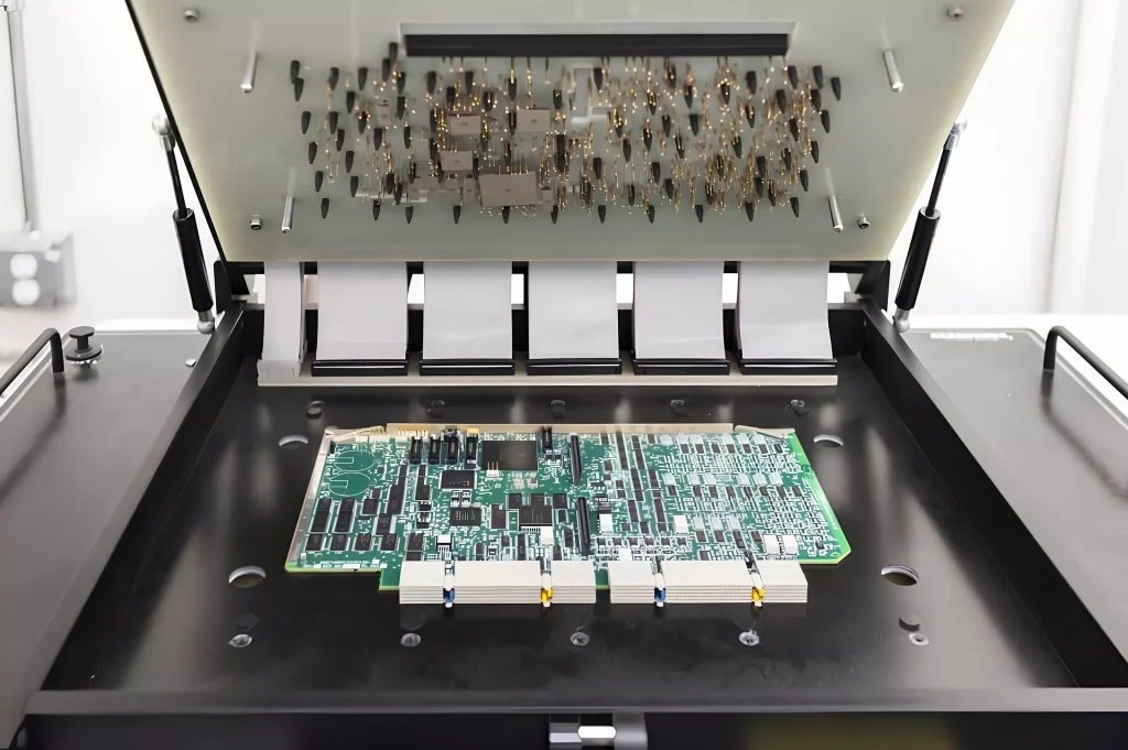
Functional Testing (FCT):
Final testing powers the completed PCB in actual or simulated operating conditions, verifying that all systems perform according to specifications. Processor boot tests, memory validation, RF transceiver calibration, and sensor verification all occur during functional testing. FCT represents the final gate before products reach consumers, ensuring that no defect reaches the field.
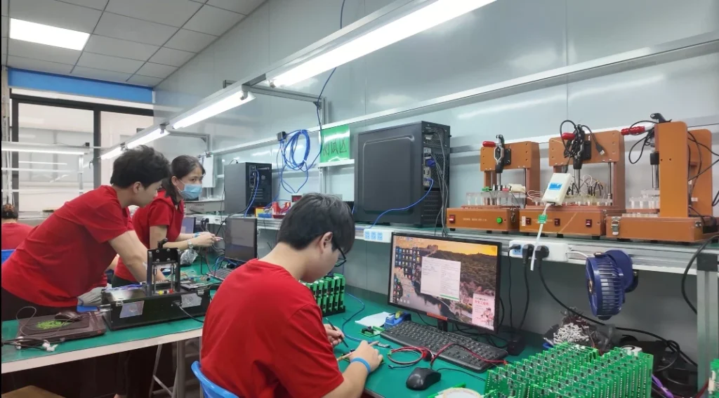
Layer-by-Layer Quality Control in Fabrication
PCB fabrication quality begins with raw material inspection and continues through every process stage.
Image Transfer and Etching Control:
After photolithography transfers the circuit pattern to copper, automated optical inspection verifies pattern accuracy. Trace width measurements confirm that etching produced traces within ±10% of design specifications. Electrical testing of bare boards (before component assembly) measures conductor continuity, insulation resistance between traces, and characteristic impedance of controlled-impedance traces.
Via Formation and Plating:
Vias connecting different layers undergo automated inspection to verify hole diameter, wall plating thickness, and internal continuity. High-speed photography can detect micro-cracks in plating that would fail under thermal cycling. Thermal cycling tests—repeatedly heating and cooling PCBs to extreme temperatures—verify that materials remain bonded and interconnections survive mechanical stresses.
Applications Across Device Categories
Mobile PCBs serve diverse device categories, each imposing unique requirements.
Flagship Smartphones
Premium devices featuring 5G connectivity, high-refresh displays, advanced cameras, and powerful processors employ cutting-edge PCB technology: 10-12 layer stacks with HDI via technology, high-thermal-conductivity substrates, and sophisticated thermal management. These devices justify higher manufacturing costs through superior performance and reliability.
5G Devices and mmWave Integration
5G smartphones operating at millimeter-wave frequencies (24-40 GHz) require entirely different RF considerations than 4G predecessors. Millimeter-wave modules dissipate significant heat, requiring specialized thermal management. Multiple antenna arrays with beamforming capability demand precise impedance matching and coupling control.
Wearable Devices and Internet-of-Things
Smartwatches, fitness trackers, and IoT devices employ simplified PCBs with 4-6 layers, trading some performance for lower cost and power consumption. These applications prioritize battery life, often selecting lower-performance processors that consume less power but operate at lower clock rates.
Folding and Flexible Devices
Innovative form factors like Samsung Galaxy Z Fold and similar devices employ sophisticated rigid-flex architectures with multiple flexible sections supporting repeated mechanical bending. These designs push manufacturing technology to its limits, requiring specialized equipment and processes available only from advanced manufacturers.

Regulatory Compliance and Industry Standards
Mobile PCBs must meet stringent regulatory requirements, ensuring safety, reliability, and environmental responsibility.
IPC-A-600 Acceptability Standards
IPC-A-600 defines visual acceptability criteria for PCB fabrication. Three class levels accommodate different application requirements:
Class 1 (General Electronics):
Suitable for non-critical consumer electronics. Allows minor cosmetic defects, provided electrical function remains intact.
Class 2 (Service Electronics):
Applied to devices requiring higher reliability—automotive, industrial, telecommunications. Defects must not compromise electrical or mechanical function, though minor cosmetic imperfections may exist.
Class 3 (High-Reliability Electronics):
Aerospace, medical, and military applications require maximum reliability. Essentially, no defects are acceptable. Inspection criteria are most stringent, requiring specialized equipment and expertise.
RoHS Compliance
Restriction of Hazardous Substances (RoHS) directives prohibit lead and other hazardous materials in electronics sold in Europe and many other regions. Compliance requires careful material selection throughout: lead-free solder (typically SAC305 alloy), components free of restricted substances, and manufacturing processes adapted for lead-free requirements.
Certification Requirements
Products destined for different markets require specific certifications: FCC certification for RF devices sold in North America, CE marking for European markets, and various country-specific certifications for other regions. These certifications verify compliance with electromagnetic interference limits, radiation safety, and electrical safety requirements.
Design-to-Manufacturing Collaboration: Ensuring Success
Effective mobile PCB development requires seamless collaboration between design teams and manufacturing partners throughout the product lifecycle.
Design for Manufacturing (DFM) Analysis
Before committing to production tooling, comprehensive DFM reviews identify potential manufacturing challenges: trace widths approaching design rule limits, vias in difficult locations, unusual material combinations, or thermal profiles beyond equipment capabilities. Early identification prevents expensive engineering changes after tooling investment.
Process Capability Documentation
Manufacturing partners should provide detailed documentation of process capabilities: minimum trace width and spacing, layer count limits, minimum via diameter, maximum aspect ratio (board thickness to smallest hole diameter), material options, and surface finish availability. Understanding these capabilities ensures designs remain within manufacturability boundaries.
Supply Chain Transparency
For products distributed globally, supply chain transparency ensures consistent quality. Traceability systems track material lot numbers, manufacturing process parameters, and component sources throughout production. This documentation enables root cause analysis if field issues emerge and supports compliance audits for regulated industries.

Frequently Asked Questions
Q: How many PCB boards are inside a smartphone, and what are they?
A: A modern smartphone is a sophisticated assembly of multiple PCBs, typically ranging from 5 to 8 in total, which work together as one integrated system. The key types include:
- Main Rigid PCB: The core system board, often a complex 12 to 16 (or more) layer HDI board. It integrates the processor, memory, and cellular modems, designed for high-density routing with thousands of components, ensuring signal integrity for high-speed data transmission and effective EMI suppression.
- Sub-Rigid PCB: Handles dedicated secondary functions like advanced camera modules, audio processing, and fast charging circuits.
- Flexible PCBs (FPCs): These thin, bendable circuits (typically 4-6 layers) connect peripherals like the display and buttons. Critical for cameras, they are engineered to fit within tight spaces, withstand repeated flexing, and manage heat to maintain stable performance during operation.
Q: What is the typical lead time for mobile PCB production?
A: Lead times vary based on design complexity and production volume.
- Simple 6-layer designs with standard materials require 4-6 weeks from design approval to mass production.
- Complex designs utilizing HDI technology or specialized materials extend lead times to 8-12 weeks.
- Prototype quantities can often be expedited to 2-3 weeks for urgent requirements.
- Custom Mobile Solution: A standard lead time of 6 to 8 months is required to bring a customized mobile phone solution from concept to mass production.
Q: How are design modifications handled once production begins?
A: Engineering change orders (ECOs) require careful management to avoid production disruptions. Minor changes to non-critical areas (such as solder mask color or silkscreen text) typically require 1-2 days of processing. Electrical changes affecting layer stack-up, via locations, or trace routing may require complete re-qualification, consuming 2-4 weeks. Early design optimization reduces the need for post-production ECOs.
Q: What quality guarantees are available?
A: Reputable manufacturers provide defect rates guaranteed below 50 PPM (parts per million) for high-volume production—meaning fewer than 50 defective units per million produced. Premium quality agreements specify even lower rates: 10-20 PPM for critical applications. These guarantees are backed by production data, statistical process control, and comprehensive traceability documentation.
Q: How does thermal management affect PCB design and cost?
A: Thermal management represents a significant cost driver for premium devices. Thermal via arrays increase fabrication complexity and cost by 15-30%. High-thermal-conductivity substrates cost 20-40% more than standard materials. However, these investments typically deliver superior performance, reduced thermal throttling, and improved battery life—justifying the additional expense for flagship products.
Q: What certifications should mobile PCBs meet?
A: At minimum, PCBs should meet IPC-A-600 Class 2 standards, ensuring consistent quality. RoHS compliance is mandatory for products sold in Europe and increasingly required globally. UL certification verifies electrical safety. For products incorporating RF functionality, FCC certification (North America) and CE marking (Europe) verify compliance with electromagnetic limits. Specific requirements vary by market and application.
Q: How are design and production processes adapted for foldable devices?
A: Foldable devices employ rigid-flex architectures with multiple flexible sections enabling repeated bending. Manufacturing requires specialized lamination equipment and processes for the sequential buildup of flex and rigid layers. Design analysis must verify that the hinge region survives the mechanical stress of 100,000+ open-close cycles. Thermal management requires careful material selection in the hinge area to avoid material degradation from repeated flexing and any heat generation.
Conclusion: Partnering for Success
Mobile PCB design and manufacturing have evolved into a sophisticated discipline requiring expertise across electrical engineering, mechanical design, materials science, and manufacturing process control. The PCBs powering today’s smartphones represent the culmination of decades of technological advancement, yet continue to push technological boundaries as new device capabilities and form factors emerge.
Selecting a manufacturing partner with demonstrated expertise in mobile PCB design, access to advanced equipment and processes, and commitment to quality excellence is essential for competitive product success. IWDF Solutions brings proven experience in mobile PCB design and production, having delivered solutions to leading global smartphone manufacturers and achieved consistent quality exceeding 98% first-pass yield.
Our capabilities encompass the full spectrum of mobile PCB technology:
- HDI design and manufacturing with blind/buried vias and microvias
- Thermal management solutions for high-power processors and 5G modems
- Signal integrity expertise for 5G frequencies and high-speed interfaces
- Rigorous quality control combining AOI, X-ray, ICT, and functional testing
- Rapid prototyping capabilities supporting design optimization and time-to-market acceleration
- Supply chain transparency and regulatory compliance documentation
For organizations developing next-generation mobile devices, we invite discussion of your specific requirements. Contact our technical team to explore how IWDF Solutions can accelerate your development timeline while ensuring the manufacturing reliability necessary for commercial success in competitive global markets.

