

You need a flexible PCB for your next product. You are not sure whether it needs to be a flex PCB or a rigid-flex PCB. The fabrication quotes look very different, and you are not sure why.
Flex PCBs and rigid-flex PCBs are not two versions of the same thing. A flex PCB is a single continuous flexible substrate — the whole board bends. A rigid-flex PCB integrates rigid FR4 sections and flexible polyimide sections into one board, replacing connectors and harnesses across multiple component zones. Choosing the wrong one affects your materials, your fabrication process, your DRC rules, and your total project cost.
This confusion does not come from PCB factories — experienced manufacturers know exactly what each technology requires. It comes from engineers and procurement teams who are specifying flex circuits for the first time, or product managers who see “flexible” in the name and assume these are interchangeable options. Before your design goes to fabrication, you need to understand what each one actually is, how each one is built, and how to decide which one your project actually needs. That is what this article covers.
What Is the Real Difference Between Flex and Rigid-Flex PCB Design?
Most specification mistakes happen because engineers skip the basics and go straight to design rules. Before comparing design approaches, you need a clear picture of what each board actually is.
Here is a straightforward breakdown of both technologies — what they are, how they are built, and where they are used.
Flex PCB
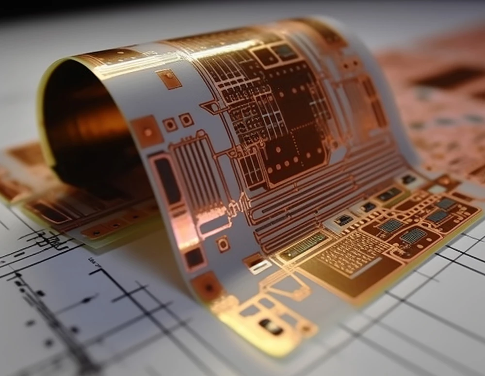
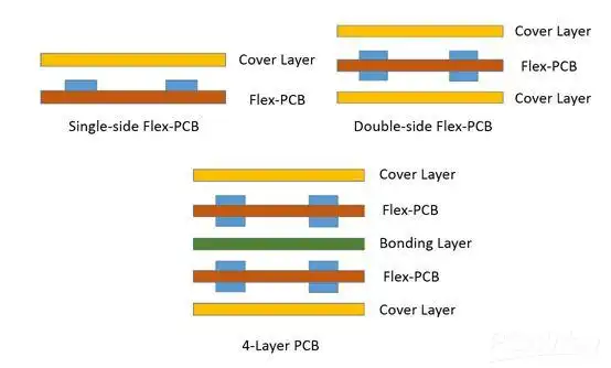
A flex PCB (flexible printed circuit, or FPC) is a circuit board built entirely on a thin, flexible polymer film — most commonly polyimide (PI). Conductive copper traces are printed or laminated onto this film, with coverlay bonded over the top as insulation. The entire board bends, folds, and twists without breaking.
Key characteristics:
- Temperature resistance: –200°C to +400°C (polyimide substrate)
- Lightweight and thin — significantly reduces assembly weight and space
- Can replace rigid PCBs, cables, and connectors in compact designs
- Supports static bending (bend-to-install) and dynamic bending (continuous flex during operation)
Typical applications: Smartphones, wearables, medical sensors, cameras, hearing aids, foldable displays, and any product where space and weight matter.
In flex PCB design terms: The whole board is flexible. Where components need to be soldered, a stiffener (FR4, polyimide, or aluminum) is bonded to the back of the flex to prevent bending at that spot. The stiffener carries no electrical signals — it is a mechanical support only.
Rigid-Flex PCB
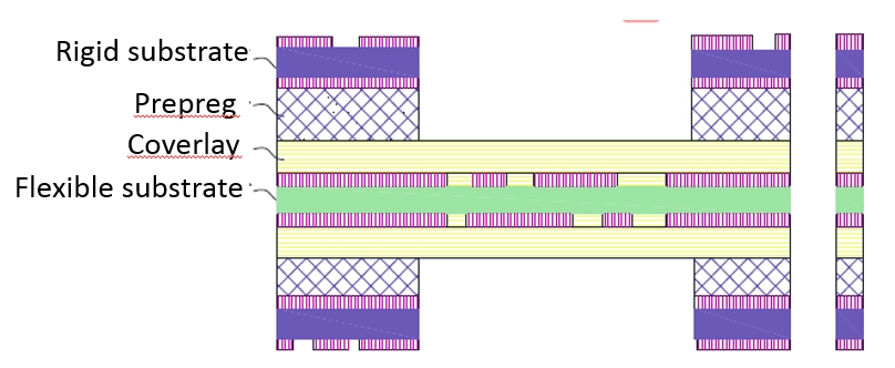
A rigid-flex PCB combines rigid FR4 sections and flexible polyimide sections into one continuous, interconnected board. The rigid sections host components. The flexible sections route circuits between them in three-dimensional space — replacing wire harnesses, board-to-board connectors, and cable assemblies.
Key characteristics:
- One board replaces multiple rigid PCBs plus all the connectors and cables between them
- Designed in 3D from the start — the folded assembly shape is part of the design, not an afterthought
- Higher layer count (4–40 layers) supports complex, high-density circuit partitioning
- Eliminates every mechanical connector between board sections, which is the most common source of field failures in high-vibration and high-reliability environments
Typical applications: Aerospace avionics, military electronics, implantable medical devices, automotive safety systems, industrial robots, and satellite subsystems.
In Rigid-flex PCB design terms: Components and vias are placed in rigid zones only. The flexible sections are routing-only zones with strict rules for trace direction, bend radius, and copper type.

The Simplest Way to Tell Them Apart
| Flex PCB | Rigid-Flex PCB | |
|---|---|---|
| What it is | A fully flexible routing medium | An integrated 3D board system |
| What it replaces | A cable or ribbon connector | Multiple PCBs + harnesses + connectors |
| Where components go | On stiffened zones (stiffener is mechanical only) | In rigid FR4 sections (electrically integrated) |
| Design space | 2D layout, defined fold lines | Fully 3D, designed in folded configuration |
| Cost vs. standard rigid PCB | +20–50% | 5–10× |
One more option worth knowing: flex PCB with stiffeners (IPC Type 1–3). This is not the same as rigid-flex. The stiffener is a mechanical layer only — it carries no signals. It adds local rigidity at connector and component zones at 40–50% lower cost than full rigid-flex. When a design does not need signal routing through a rigid substrate, this is often the right answer.
Now you know what each board is and where it belongs. But knowing the technology type is only the first step. The performance of a flex or rigid-flex PCB — how long it lasts, whether it survives bending, whether it passes thermal cycling — is determined before a single trace is placed. It comes down to four material decisions that most engineers either make by default or leave to the supplier. Getting any one of them wrong produces boards that look correct at inspection and fail in the field.
Do Your Materials Actually Match What the Design Requires?
Most flex and rigid-flex field failures do not come from routing errors. They come from material decisions made — or left as default — before layout began.
Four material choices determine whether your flex or rigid-flex PCB survives its intended operating environment: substrate type, copper grain structure, outer insulation type, and prepreg selection at the rigid-to-flex boundary. Each one has a specific failure mode if chosen incorrectly — and most of those failures pass incoming electrical inspection.
Substrate: Polyimide Is Not Optional for Soldered Designs
Polyimide (PI) is the correct substrate for any flex or rigid-flex PCB that goes through SMT assembly. It handles temperatures from –269°C to +400°C continuously, with a stable dielectric constant of Dk 3.2–3.5 across frequency and temperature. It accounts for approximately 85% of all FPC applications.
Polyester (PET) costs about 30% less and is appropriate for non-soldered applications only — membrane keypads, RFID antennas, and flat cables terminated by pressure contact. It degrades above 105°C and cannot survive reflow. If a supplier quotes a soldered flex design in PET without flagging it, that is a material error that needs to be corrected before any files go to production.
Copper Type: One Wrong Decision, Thousands of Field Returns
Rolled-annealed (RA) copper is made by mechanically rolling copper into foil. This aligns the grain structure parallel to the rolling direction. That structure allows the copper to bend repeatedly with very low fatigue accumulation. RA copper is mandatory for any dynamic flex application — any design that will bend more than 100 times in service.
Electrodeposited (ED) copper is produced by electroplating. It has higher tensile strength, lower cost, and is the right choice for static flex applications and the rigid sections of rigid-flex boards.
The failure mode when ED copper is used in a dynamic flex zone: the board passes all incoming inspection, works normally for weeks or months, then develops intermittent opens as copper fatigue fractures grow outward from the bend zone. These failures do not reproduce reliably on a test bench. They arrive as field returns.
In rigid-flex PCB design, one board needs both: RA copper in flex sections, ED copper in rigid sections. A fabricator using one copper spec across the whole board has not understood the design.
Coverlay vs. Flexible Solder Mask: Not the Same Material
On rigid PCBs, solder mask is a surface coating. On flex and rigid-flex PCBs, the outer insulation in flex zones is a structural component. The wrong choice reduces service life in ways invisible at incoming inspection.
Polyimide coverlay is a solid PI film bonded to the copper under heat and pressure. It provides approximately 3 kV dielectric withstanding voltage per 0.001″ of thickness, creates an impermeable environmental seal, and maintains mechanical integrity through repeated bending. The minimum pad-to-pad dam is 10 mils. For any dynamic flex application or harsh operating environment, coverlay is the correct specification.
Flexible solder mask is a liquid epoxy with flex additives — 10–30 microns thick. It allows a tighter pad-to-pad dam of 4 mils, enabling finer-pitch SMT pad definition than coverlay pre-windowing can achieve at fine pitches. It is appropriate for static flex designs with fine-pitch components. It is not a substitute for coverlay in dynamic or environmentally demanding designs.
On a rigid-flex PCB, the correct specification uses both: coverlay in flex zones, solder mask on rigid zones. A supplier applying solder mask across the entire board — including flex sections — has reduced the board’s service life without disclosing it.
No-Flow Prepreg: The Fabrication Detail That Reveals Real Competence
Standard PCB prepreg contains high-flow resin. In a rigid-flex stack-up, that resin migrates into the flex zone during lamination pressing. It contaminates the polyimide, increases local stiffness at the material boundary, and creates a stress concentration point that initiates cracking under mechanical load.
The correct material at every rigid-to-flex boundary is no-flow or low-flow prepreg. No-flow prepreg costs $1.50–$3.00 per square foot. Standard high-flow prepreg costs about $0.25. That is a 6–12× cost difference.
A rigid-flex quotation priced at standard rigid PCB levels is not a competitive offer. It is a sign that the supplier is using the wrong materials — and the boards will look correct at inspection and fail in the field.
With the right materials specified, you have set the physical ceiling for what your board can do. But materials alone do not prevent field failures. A flex PCB built with the correct polyimide substrate and RA copper will still crack, delaminate, or develop intermittent opens if the layout ignores how those materials behave under repeated bending. That is what design rules are for — they translate material properties into specific, measurable constraints on trace routing, bend radius, via placement, and pad geometry. Miss one, and the board fails in ways that pass every incoming inspection.
What Are the Design Rules for Flex PCB Design?
A flex PCB that passes DRC and electrical test can still fail in service. The rules that prevent this are different from anything in standard rigid PCB design — and they cannot be assumed from FR4 experience.
Every layout decision in the flex zone exists to prevent copper fatigue failure under repeated bending. The foundation of all of it is the static vs. dynamic classification.
Static vs. Dynamic: Decide This Before Placing a Single Trace
A static flex application bends fewer than 100 times over the product’s lifetime — a camera module cable folded once during assembly, a sensor tail routed through a housing. A dynamic flex application bends continuously during operation — robotic joint cabling, 3D printer gantry ribbons, laptop hinge interconnects. This classification determines copper type, bend radius multiplier, via rules, and stiffener selection. Designing a dynamic application to static standards produces a board that works at first and fails in the field.
Bend Radius: The Formula That Prevents Copper Fatigue
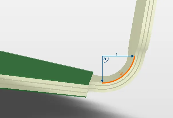
Minimum safe bend radius: R = T × N
- R = minimum bend radius
- T = total flex thickness (all copper, PI, adhesive, and coverlay combined)
- N = multiplier by layer count and application type
| Construction | Application | N Multiplier |
|---|---|---|
| Single-layer flex | Static | 6–10× T |
| Double-layer flex | Static | 10–15× T |
| Multilayer flex (3+ layers) | Static | 20× T or more |
| Single-layer flex | Dynamic | 15× T minimum |
| Double-layer flex | Dynamic | 20× T minimum |
| Rigid-flex flex zone | Dynamic, heavy load | 25× T |
Example: a double-layer dynamic flex section with total construction thickness of 250 µm needs a minimum bend radius of 20 × 250 µm = 5 mm. Violating this does not produce immediate failure. Fatigue accumulates cycle by cycle until a trace fractures — after the product has shipped. Every bend location must be explicitly dimensioned on the fabrication drawing with its minimum radius and expected cycle count.
Trace Routing, Via, and Pad Rules
Four trace routing rules apply to every flex zone:
- Run traces perpendicular to the bend axis. Parallel traces are strained across their full length with every bend. Perpendicular traces are strained only across their width — far lower cumulative fatigue.
- Eliminate all 90° angles. Sharp corners concentrate bending stress at a single point. Smooth curves distribute stress over a longer path.
- Stagger traces on multilayer designs. Traces on adjacent layers stacked directly over each other create an I-beam cross-section — dramatically stiffer, higher stress, shorter service life. Offset them laterally.
- Keep traces narrower in the flex zone. Wider traces have higher bending stiffness. Use the minimum width that meets current-carrying requirements.

No vias in dynamic flex zones. This is an absolute rule. Plated through-hole barrels in bending zones crack under shear forces. Small fractures grow with each flex cycle until the signal path fails — and this failure passes room-temperature electrical testing.
Teardrop vias are mandatory for traces below 20 mils connecting to a via pad. The teardrop geometry widens the trace gradually into the pad, eliminating the stress riser at the junction that would otherwise initiate fatigue cracking.
Pad anchors (spurs) are small copper extensions from pad perimeters, encapsulated under the coverlay opening. Copper-to-PI adhesion is weaker than copper-to-FR4. Without pad anchors, pads peel from the substrate during handling or assembly — late enough to be expensive.
Stiffener Selection: Put Rigidity Where the Design Needs It
| Stiffener Material | Primary Function | Typical Use Case |
|---|---|---|
| FR4 (0.010″–0.059″) | Mechanical support for SMT + PTH | Connector zones, pick-and-place reference surface |
| Polyimide | Tight stack-height compliance | ZIF connector interfaces |
| Aluminum | Heat dissipation + rigidity | Power components, LED assemblies |
| Stainless steel | Abrasion/chemical resistance | Medical instruments, sensors exposed to contact |
What Are the Design Rules for Rigid-Flex PCB Design?
Knowing flex PCB design rules does not prepare you for rigid-flex. The disciplines overlap in some areas, but rigid-flex introduces problems with no equivalent in pure flex design — dissimilar material interfaces under thermal load, 3D design from the first session, and a transition zone that generates most of the field failures in this product category.
IPC Standards You Must Know
IPC-2223 is the primary design reference for rigid-flex PCB design. It governs bend radii by layer count, via and pad geometry in flex zones, impedance control, and the performance class criteria that determine inspection and test requirements.
| Standard | What It Governs |
|---|---|
| IPC-2223 | Design rules: bend radii, via/pad geometry, zone definitions, impedance |
| IPC-4202 | Flexible base dielectric materials |
| IPC-4203 | Coverlay and bonding materials |
| IPC-6013 | Performance specification — Classes 1, 2, 3 |
| MIL-P-50884 | Military specification for flex/rigid-flex boards |
IPC Class 3 — for medical devices, defense, and aerospace — imposes the tightest requirements on annular ring dimensions, copper plating thickness, void inspection, and electrical test coverage. A supplier who cannot specify which IPC class their process targets is not a credible partner for any demanding rigid-flex application.
Stack-Up: The Foundation of Every Other Design Decision
The rigid-flex stack-up must be defined with the fabricator before layout starts — not submitted with the Gerber package. Different factories have different process constraints, and a stack-up that is theoretically valid per IPC-2223 may be impossible to build in a specific facility.
Flex core: Adhesiveless polyimide laminates are the professional standard. Adhesive-based constructions introduce material layers that expand non-uniformly during lamination, creating Z-axis stress that causes delamination during thermal cycling. Adhesiveless constructions are 12–25 µm thinner per flex layer, which directly enables tighter bend radii.
Rigid layers: High-Tg FR4 with Tg > 170°C, matched to the polyimide cure temperature. CTE mismatch greater than 20 ppm/°C between rigid and flex materials at the bonding interface causes interlayer cracking during reflow or field thermal cycling — invisible at room-temperature inspection, fatal in service.
Prepreg at the rigid-to-flex boundary: No-flow or low-flow only. Resin contamination of the flex zone increases local stiffness and creates a stress concentration point that initiates cracking under load.
Three Layout Rules With No Exceptions
All components must be in rigid sections only. Any component placed in a flex zone or transition zone will have its solder joints stressed by every bend cycle and every thermal expansion event. The failure — intermittent opens — will not reproduce on a test bench. It arrives as a field return.
All vias must be in rigid sections only. Minimum clearance from any via center to any flex zone boundary is 0.5 mm. Via barrels in or near flex zones crack under shear forces. The failure passes ambient electrical test and becomes an intermittent fault under thermal or mechanical stress.
No 90° bends anywhere. A perpendicular bend concentrates stress at a line across the full board width. No bend radius specification compensates for this geometry. The only acceptable approach is a gradual arc that spreads deformation across the full flex section length.
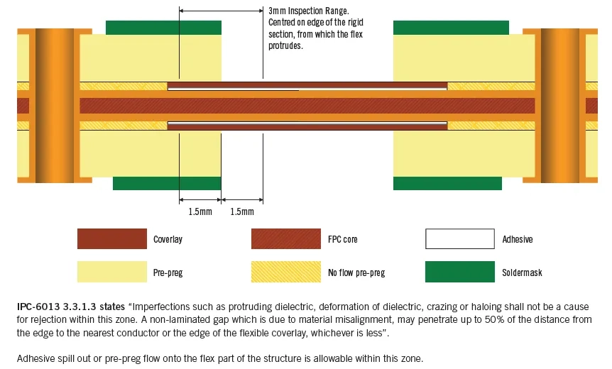
Transition Zone: Where Most Rigid-Flex Failures Start
The transition zone — where FR4 rigid material ends and polyimide flex is exposed — is the highest-stress location in any rigid-flex assembly. Two dissimilar materials with different elastic moduli and different CTE values meet at a defined boundary. Under mechanical or thermal loading, that boundary concentrates stress.
Managing this requires:
- Gradual tapers and radius fillets at the material boundary — stress is distributed over a longer path, not concentrated at a sharp edge
- Strain relief slots or cutouts flanking the flex zone entry — these absorb relative motion before it reaches conductive traces
- No via or pad within 0.5 mm of the transition boundary
- Solid copper fills on the neutral axis layer through the flex zone — the layer closest to the geometric center, where bending stress is lowest
- No copper on the outer tension surface at the flex zone entry — tensile stress is highest there during bending
DRC Customization Is Not Optional
Standard PCB DRC applies uniform constraints across the entire board. For rigid-flex, that is wrong. Separate rule sets must be configured for rigid sections, flex sections, and transition zones. Design tools — Altium Designer, Cadence Allegro, Mentor Xpedition, Zuken CR-8000 — all support this, but the rules must be explicitly set. They are never defaults.
Minimum custom DRC rules for rigid-flex:
- Via obstruct regions covering all flex and transition zones
- Component placement obstruct for flex and transition zones
- Enlarged annular ring requirements in flex zones (20–25% larger than rigid minimums)
- Solid copper fill enforcement in bend zones (no hatched fills)
- Minimum 0.5 mm trace-to-edge clearance in flex zones
- Impedance constraint regions for all controlled-impedance traces through the transition zone
A design that passes default rigid PCB DRC has not been verified for the features that determine whether a rigid-flex board survives in service.
How Do You Decide Between Flex PCB and Rigid-Flex PCB Design?
The technology choice is a product engineering decision — not a supplier capability question. Getting it right early saves budget, protects reliability, and prevents re-spins.
Here is the decision framework we apply at IWDF Solutions on every client project:
Choose flex PCB design when:
- The application requires continuous dynamic bending — robotic joints, printer gantry ribbons, foldable device hinges. Pure flex with RA copper and proper bend radii is optimized for this. Rigid-flex is not.
- The circuit fits within 1–4 layers and does not need multi-section component hosting. Consumer electronics, wearables, medical sensors, and display cables all fit this profile.
- Production volumes are high and unit cost is the dominant variable. Flex PCB tooling and material costs scale better at volume.
- The design has one or two PCB sections connected by a ribbon cable. Redesigning as rigid-flex does not return the investment at this scale.

Choose rigid-flex PCB design when:
- The product requires multiple component-bearing sections interconnected without board-to-board connectors. Every connector eliminated removes an interconnect failure point. For four or more PCB sections, rigid-flex typically reduces total system cost despite higher per-board cost.
- The product operates under high shock, high vibration, or extreme environments — aerospace avionics, military electronics, automotive safety systems. The integrated construction eliminates connector failure modes under vibration. Rigid-flex assemblies have demonstrated up to 60% weight reduction vs. equivalent rigid PCB plus harness assemblies in aerospace applications.
- 3D packaging geometry cannot accommodate flat PCBs — implantable medical devices, satellite subsystems, in-ear instruments, compact avionics. Rigid-flex allows the board to be designed in folded configuration from the start.
- Long service life and IPC Class 3 reliability are required. For medical, defense, and critical industrial applications, the interconnect reliability of a rigid-flex PCB built to Class 3 standards cannot be matched by connector-based assemblies over equivalent service lifetimes.

Cost Reference for Engineering Planning
| Technology | Typical Cost / sq. in. | vs. Standard Rigid PCB |
|---|---|---|
| Standard rigid PCB (FR4, 4-layer) | $0.15–$0.40 | Baseline |
| Flex PCB (1–2 layer, PI) | $0.50–$8.00 | +20–50% |
| Flex PCB (multilayer, 3–6 layers) | $5.00–$15.00 | 2–5× |
| Rigid-flex PCB (4-layer) | $3.00–$5.00 | 5–7× |
| Rigid-flex PCB (6+ layers) | $7.00–$25.00 | 8–15× |
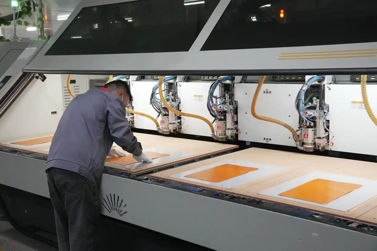
The rigid-flex cost premium comes from no-flow prepreg (6–12× the cost of standard prepreg), laser routing to expose flex zones, lower panelization efficiency, higher lamination scrap rates, and a longer manufacturing cycle. A rigid-flex quotation priced at standard rigid PCB levels is not competitive. It means the wrong materials are being used.
What Should Overseas Clients Verify Before Sourcing From a China PCB Manufacturer?
Shenzhen’s manufacturing ecosystem is unmatched in supply chain density. PI laminates, RA copper foil, and no-flow prepreg are available within days. Fast-turn prototypes and rapid production ramp support that take weeks elsewhere happen in days here. But this density also means wide variation in supplier capability — and for flex and rigid-flex PCB design and fabrication, that variation shows up not at incoming inspection, but at 50,000 flex cycles or after the fifth thermal shock cycle in the field.
What Certifications Actually Tell You
ISO 9001 confirms that the supplier follows documented processes. It says nothing about the technical quality of those processes. Every supplier worth evaluating holds ISO 9001.
IATF 16949 is the automotive quality standard. It requires documented process capability (Cpk), measurement system analysis (MSA), and failure mode analysis (FMEA). A supplier holding IATF 16949 has demonstrated the process discipline that automotive-grade flex and rigid-flex manufacturing requires.
ISO 13485 covers medical device quality management. For any flex or rigid-flex PCB destined for a medical application, ISO 13485 is the minimum quality system requirement. Ask whether the supplier can also discuss biocompatibility compliance and device history record (DHR) management.
IPC-6013 Class 3 production capability is separate from quality management certification. Ask directly: can the supplier provide production test data demonstrating IPC-6013 Class 3 compliance — annular ring dimensions, copper plating thickness measurements, void inspection results? A supplier who cannot answer with specific production data is not building Class 3 boards regardless of what their certificate wall says.
Five Questions That Reveal Real Technical Competence
- “What prepreg do you use at the rigid-to-flex boundary, and what is its resin flow specification?” The correct answer is no-flow or low-flow prepreg with documented resin flow data. Any other answer is a red flag.
- “What is your minimum bend radius capability, and how do you verify it in production?” A credible answer specifies radius by layer count and application type and describes a verification process — not just “we follow the customer spec.”
- “Can you provide impedance measurement data showing ±10% tolerance across a rigid-to-flex transition?” This is a process discipline requiring dedicated measurement protocols. A supplier who can provide this data has actually solved the problem.
- “Do you have in-house PCB design engineers who review customer files for DFM before fabrication?” Fabricators who process Gerber files without DFM review cannot catch bend radius violations, via placement errors in flex zones, or stack-up definitions incompatible with their lamination process — until those problems cause yield failures.
- “Are your prototypes built on production equipment with production materials?” A factory that uses different equipment or materials for prototypes than for production makes its engineering validation unreliable.
Why One-Stop Service Matters More for Flex and Rigid-Flex?
For standard rigid PCBs, the handoff between PCB design, fabrication, and assembly is manageable. For flex and rigid-flex boards, every handoff is a failure point. Design intent that is clear to the engineer who built the stack-up becomes ambiguous when a separate fabricator interprets the file package. A DFM issue caught during fabrication requires design re-entry if the design team is in a different organization.
At IWDF Solutions, the same engineering team that designs or reverse-engineers the flex or rigid-flex PCB also oversees its fabrication and PCBA production. The engineers who made each design decision are the same people who supervise its execution on the production floor. There is no translation gap between design intent and manufacturing reality — and for flex and rigid-flex PCB production, that gap is where most problems live.
For PCB reverse engineering and PCB cloning projects involving flex or rigid-flex boards, our process includes layer-by-layer physical analysis, material identification, complete stack-up reconstruction, and full schematic capture — producing documented BOMs and schematics that allow clients to modify, improve, and scale-produce the design under their own engineering control.
If you are evaluating PCB design partners, PCB manufacturers, or PCBA suppliers for a project involving flex PCB design or rigid-flex PCB design, send us your project specifications, requirements, existing board files, or physical samples. Our engineering team will respond with a technical assessment of your project requirements — not a generic quotation template.
FAQ: Flex PCB and Rigid-Flex PCB Design
Q: Can I place SMT components directly on a flex PCB without a stiffener?
Technically yes, but it is not reliable in practice. Without a stiffener, the SMT pads and solder joints experience every bending load applied to the flex substrate. This leads to solder joint cracking and pad delamination under repeated flexing or handling. Any zone hosting SMT components should be stiffened — typically with FR4 or polyimide — to prevent bending at that location entirely.
Q: What is the minimum bend radius I can achieve with a single-layer flex PCB?
For a static application, a single-layer flex PCB with adhesiveless polyimide construction and RA copper can achieve bend radii as tight as 1–2 mm, depending on total construction thickness. For dynamic applications, the minimum safe radius is 15× the total construction thickness. A 100 µm thick single-layer construction in a dynamic application needs a minimum radius of 1.5 mm — and that requires adhesiveless laminate, RA copper, and no vias anywhere in the bend zone.
Q: Is rigid-flex always more expensive than flex PCB with stiffeners?
Yes, in nearly all cases. Full rigid-flex PCB construction is typically 3–5× the cost of a comparable flex PCB with stiffeners. The rigid-flex cost premium comes from no-flow prepreg, laser routing, lower panelization efficiency, and a longer manufacturing cycle. Flex with stiffeners is the right answer whenever the design does not require electrical signal routing through a rigid substrate across multiple board sections.
Q: How many layers can a rigid-flex PCB have?
Rigid-flex PCBs support 4–40 layers. Practical designs most commonly fall in the 4–16 layer range, where the flex core carries 2–4 layers and the rigid sections add additional layers as needed. Layer count beyond 20 is uncommon and typically reserved for high-density defense or aerospace applications with stringent space and weight constraints.
Q: What IPC standard should I specify for my rigid-flex PCB design?
IPC-2223 governs the design of flex and rigid-flex PCBs. IPC-6013 governs the performance and acceptance criteria. For consumer and industrial applications, IPC Class 2 applies. For medical devices, aerospace, military, and any application where service interruption is unacceptable, IPC Class 3 applies. Specify the class in your design documentation and confirm your fabrication partner’s capability before committing to production.
Q: Can rigid-flex PCBs be used for high-speed designs above 1 GHz?
Yes, but it requires careful management of the rigid-to-flex transition zone. At frequencies above 500 MHz, the change in dielectric constant from FR4 (Dk 4.2–4.5) to polyimide (Dk 3.2–3.5) creates impedance discontinuities that cause signal reflections and timing errors. Managing this requires trace width adjustment in the flex section, continuous reference planes through the transition zone, no via transitions at the material boundary, and electromagnetic simulation to verify impedance continuity across the full trace path.
Q: What is the difference between a dynamic and a static flex PCB application?
A static flex application bends fewer than 100 times over the product’s service life — typically just once during installation. A dynamic flex application bends continuously during operation, often tens of thousands to millions of cycles. The distinction drives copper type (ED for static, RA for dynamic), bend radius multiplier, via placement rules, and layer count decisions. Designing a dynamic application to static standards is the most common cause of flex PCB field failures that pass incoming inspection.
Q: How do I know if my design needs full rigid-flex or just flex with stiffeners?
Ask one question: does my design require electrical signal routing through a rigid substrate connecting two or more component-bearing sections? If yes, you need rigid-flex. If your design only requires local mechanical support at connector and component zones, with all inter-section routing on the flex core, flex with stiffeners is sufficient — at 40–50% lower fabrication cost.

