

RF PCB designs most often fail not on the bench — but in fabrication. The gap between a working schematic and a manufacturable RF board is wider than most engineers expect.
RF PCB design requires decisions across material selection, impedance control, layer stack-up, and layout strategy — all before a single trace is routed. This guide covers the practical criteria used by experienced RF PCB designers and Shenzhen manufacturers to take an RF design from first trace to production-ready files without signal integrity surprises.

The reason RF PCB design is hard isn’t complexity for its own sake. It’s that every decision made at the layout stage shows up as a physical performance limitation in the manufactured board. To avoid that, you need to know which decisions matter most — and in what order they should be made.
What Is an RF PCB?
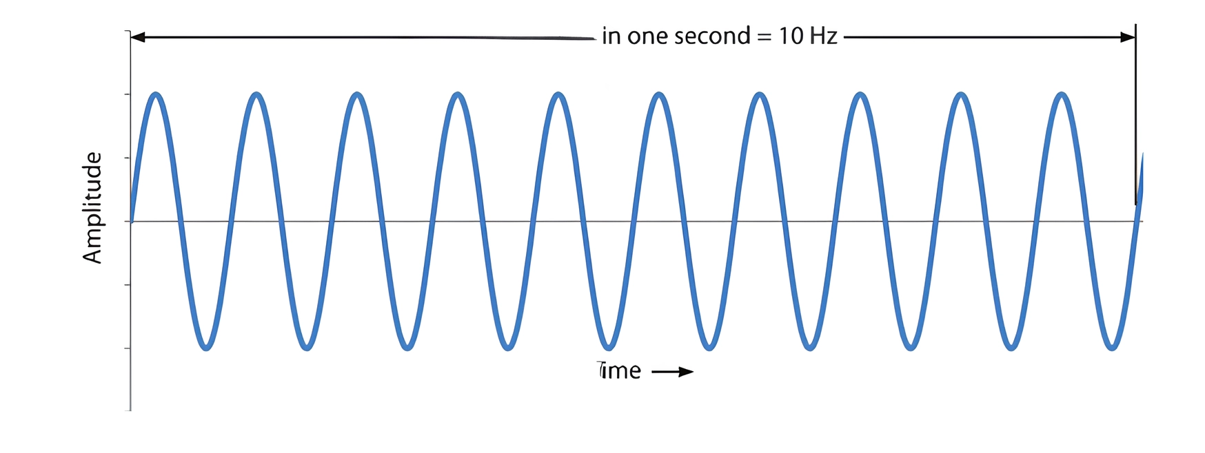
An RF PCB (Radio Frequency printed circuit board) is a specialized circuit board designed to transmit, receive, or process high-frequency signals — typically operating between 500 MHz and 100 GHz. Unlike a standard PCB, an RF PCB uses purpose-built materials such as Rogers or PTFE (Teflon-based laminates) to minimize signal loss, maintain precise impedance control across the board, and handle the thermal stress that comes with continuous high-frequency operation. These boards are the foundation of 5G infrastructure, automotive radar, aerospace communication systems, satellite equipment, and industrial RF transceivers — anywhere signal integrity and transmission accuracy are non-negotiable.
How Is It Different from a Regular PCB?
On a standard PCB, a trace is a wire. It connects two points. As long as it carries the current without burning, it works. The board material, trace length, and layer arrangement are secondary concerns.
On an RF PCB, a trace is not a wire. It is a transmission line. Its width, the material beneath it, and the distance to the ground plane below it all determine its impedance — and that impedance determines whether the signal passes through cleanly or bounces back. A trace that is 0.1 mm too narrow can reflect enough energy to fail a regulatory test or degrade system range by several decibels. The board itself is part of the circuit.
That is the practical difference. And it changes everything about how the design process works.
Where the Two Design Processes Actually Diverge
On a standard PCB, you can finalize the schematic, pick a generic FR4 board, and start routing. The board material is a background detail.
On an RF PCB, material selection and stack-up must be decided before routing starts. Change the dielectric thickness after routing is complete, and recalculate every controlled-impedance trace. Changing the material produces the same result. This is not a rule someone invented — it is a consequence of how high-frequency signals interact with physical geometry.
| What You Are Deciding | Standard PCB | RF PCB |
|---|---|---|
| What a trace does | Carries current from A to B | Acts as a transmission line with a defined impedance |
| Board material | FR4, almost always | Chosen by frequency, loss requirement, and Dk stability |
| Ground plane | Good practice, often optional | Mandatory — it is the return path and impedance reference |
| Trace width | Set by current rating | Set by target impedance (usually 50 Ω) |
| Via placement | Wherever needed | Affects impedance — every RF via is a potential reflection point |
| Routing order | Flexible | RF signal chain must be routed first, always |
| Manufacturing tolerance | ±0.1 mm generally fine | ±0.025 mm on RF traces; tighter for millimeter-wave designs |
A Concrete Example: The Same Trace at Two Frequencies
Take a 20 mm trace on a standard 4-layer FR4 board.
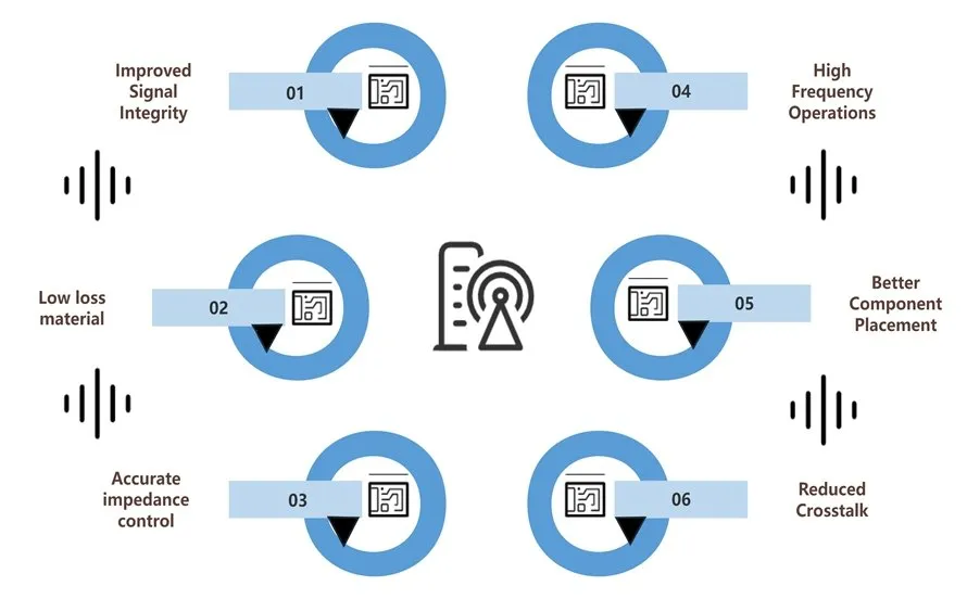
At 10 MHz, that trace has no measurable effect on the circuit. Its electrical length is a tiny fraction of the signal wavelength. It is, for all practical purposes, a short circuit.
At 5 GHz, the wavelength inside FR4 is roughly 30 mm. That same 20 mm trace is now two-thirds of a wavelength long. Depending on how it is terminated, it behaves like an antenna, a resonant stub, or a low-pass filter section — none of which you intended.
This is not a corner case. It is the normal behavior of high-frequency signals on physical conductors. RF PCB design guidelines exist specifically to control these effects — to make the board do what you intended, not what physics defaults to.
With that difference understood, the next question is practical: where exactly does an RF PCB layout begin? The answer is not where most designers start.
Where Should You Start RF PCB Design? Signal Flow, Zoning, and Isolation
Most RF PCB layout problems don’t come from bad routing. They come from a bad starting point — components placed before signal flow is mapped, domains mixed without clear boundaries, and isolation treated as an afterthought.
The correct starting point for any RF PCB layout is a functional zone map, not a component placement. Before anything goes on the board, you define where each circuit domain lives, how signals flow between them, and where the hard boundaries are. Every routing and placement decision that follows is built on that map — which is why getting it wrong at the start is so expensive to fix.

Step One: Define Your Functional Zones
An RF PCB must be divided into clearly separated functional zones before any component is placed. The four zones that apply to almost every RF design are:
- RF zone: Front-end circuits — LNA, PA, mixer, RF filter, antenna feed
- High-speed digital zone: MCU, DSP, memory, high-speed interfaces
- Analog zone: ADC/DAC, sensors, low-frequency signal conditioning
- Power management zone: DC-DC converters, LDOs, bulk capacitors, ferrite beads
Each zone gets its own physical area on the board. Between each zone, there must be a clear isolation gap — a strip of board with no traces, no vias, and no copper fills other than the ground plane. That gap is not wasted space. It is what prevents energy from coupling from one domain into another.
| Zone | Placement Location | Isolation Requirement |
|---|---|---|
| RF front-end | Adjacent to antenna or RF connector | Hard gap from all other zones; ground stitching on all boundaries |
| PA / driver stage | Within RF zone, output side | Minimum 10–15 mm from LNA input; shielding can footprint recommended |
| High-speed digital | Opposite end of board from RF zone | Ground barrier + stitching vias along full boundary |
| Analog (ADC/DAC, sensors) | Between RF and digital zones if needed | Separate ground island, single-point tie to main GND |
| Power management | Board edge or bottom layer pour | Ferrite bead isolation on every supply feeding an RF stage |
Step Two: Fix the RF Signal Flow Direction — and Don’t Cross It
Once zones are defined, the RF signal path must run in a single direction across the board. Input enters from one side, passes through each RF stage in sequence, and exits at the output. That path should never double back, cross itself, or run parallel to another section of the same chain.
This rule exists for one reason: self-oscillation. If the PA output runs anywhere near the LNA input — even with a ground plane between them — there is a coupling path. At high gain levels, that coupling becomes a feedback loop. The board oscillates. No amount of component tuning fixes a layout-level feedback path.
In practice, this means:
- Route the RF chain left to right, or top to bottom — pick one and hold it.
- Place the PA output on the opposite side of the board from the LNA input.
- If the design requires the signal to change direction, use a shielded section or a physical barrier (shielding can be provided via fence) at the transition.
Step Three: Separate Power Supplies by Domain — Not Just by Decoupling
A shared power rail is a coupling path. Two RF stages that share a supply line without proper isolation will inject noise into each other through that rail — even if both are well-decoupled locally.
Each RF domain needs its own supply:
- The LNA stage gets a dedicated low-noise LDO, placed as close as possible to the device.
- The PA stage gets a bulk capacitor before a ferrite bead, then a local decoupling capacitor after it — two-stage filtering that physically prevents PA switching noise from reaching the LNA supply.
- The digital section gets a completely separate filtered rail. Under no circumstances should a digital power rail and an RF power rail share a trace segment before their respective decoupling networks.
Why the Isolation Gap Is Non-Negotiable?
A common mistake is treating zone separation as a routing preference — something to do when space allows. It is not. Coupling between zones does not require direct electrical connection. It happens through the substrate, through shared ground plane currents, and through radiated fields.
The isolation gap forces signal paths to stay within their zone. Stitching vias along zone boundaries creates a low-impedance wall in the ground plane that blocks ground current from one domain from flowing into another. Without those vias, the “solid ground plane” beneath your RF traces is not solid at all — it is carrying noise from the digital domain directly into your RF return path.
With the zone map fixed and isolation boundaries defined, the next decision is the one that ties everything together physically: impedance control.
Impedance Control: The Make-or-Break Factor in RF PCB Design
Impedance mismatches reflect energy back into the source. In RF systems, even a small mismatch causes power loss, gain compression, and noise figure degradation. Getting impedance right starts with trace geometry — not component tuning.
Controlled impedance in RF PCB design means selecting trace width, spacing, and substrate thickness to hit a defined target — usually 50 Ω. That target must be agreed with your PCB manufacturer before layout begins, because fabrication tolerances directly determine whether your as-built board matches your simulation.
What Defines Trace Impedance?
Four parameters define microstrip impedance: trace width (W), trace thickness (T), dielectric height (H), and dielectric constant (Dk) of the substrate.
Change any one of them and impedance changes. This is why stack-up and material selection must happen before routing — not after.
A practical example: on a standard 4-layer FR4 board with a 0.2 mm core between layers 1 and 2, a 50 Ω microstrip trace on the top layer is roughly 0.35–0.45 mm wide. Change that core to 0.3 mm and the same trace needs to be wider to maintain 50 Ω. Your layout files become incorrect the moment the stack-up changes.
This is the key point: all four impedance-defining parameters come directly from your stack-up specification. The trace width is the only one you control in layout. The other three — dielectric height, Dk, and copper thickness — are determined by the laminate and layer structure your manufacturer builds. That is exactly why the stack-up must be locked before a single RF trace is routed.

Why the Stack-Up Must Be Locked Before Routing Starts
PCB manufacturers control laminate thickness, copper weight, and press cycles. These all have tolerances — typically ±10% on dielectric thickness and ±10% on copper weight.
That means your impedance can vary ±5–8 Ω from the nominal value even on a well-made board. For RF circuits, that is significant. A 50 Ω line that builds at 58 Ω causes a measurable reflection at every connector and component transition.
To manage this:
- Specify your target impedance (e.g., 50 Ω ±10%) on your fabrication drawing.
- Agree on the full stack-up with your manufacturer before you finalize the layout.
- Request impedance test coupons on the fabrication panel — they verify actual Dk and trace geometry after etching, using TDR measurement.
At IWDF Solutions, we review every RF stack-up before production starts and provide TDR-verified controlled impedance manufacturing. Getting this wrong after fabrication has no fix — the board must be re-spun.
Once the stack-up is locked and your impedance targets are defined, the next decision is which transmission line structure to use on which layer. That choice depends on your frequency, your layer arrangement, and how much radiation your application can tolerate.
Microstrip, Stripline, or CPW — Which One for Your Design?
These three transmission line types are not interchangeable. Each one suits a different combination of frequency range, layer position, and manufacturing constraint. The stack-up you just locked determines which options are available to you.
| Transmission Line | Location | Best For | Watch Out For |
|---|---|---|---|
| Microstrip | Outer layer (top or bottom) | Most RF designs below 10 GHz; easy to probe and tune | More radiation; solder mask loading affects Dk |
| Stripline | Inner layer, between two GND planes | Shielded paths; designs above 10 GHz needing low radiation | Via transitions needed; harder to probe during debug |
| Coplanar Waveguide (CPW) | Outer layer with adjacent GND pours | IC launches at mmWave; compact RF modules | Requires very tight gap control in fabrication |
For most RF PCBs below 6 GHz, microstrip is the practical default. It is accessible, simulatable, and manufacturable without exotic stack-ups. Above 10 GHz, stripline or CPW becomes necessary — microstrip radiates too much and its impedance becomes harder to control as wavelengths approach trace dimensions.
The choice between these three is not a preference. It follows directly from your frequency, your layer count, and the isolation requirements between your RF stages — all of which are already defined by the stack-up you locked in the previous step.
RF PCB Material Selection: Why FR4 Is Often Not Enough
FR4 is cheap, widely available, and works well at low frequencies. But at RF frequencies, its dielectric loss makes it the wrong choice for many applications — and the damage is invisible until you measure the board.
FR4 has a dielectric loss tangent (Df) of 0.020–0.025 and an inconsistent Dk ranging from 3.8 to 4.8. For RF PCB design above 1–2 GHz, this causes measurable signal attenuation and impedance inconsistency. Choosing the right RF laminate depends on frequency band, performance requirements, and acceptable manufacturing cost.
Key Material Properties That Affect RF Performance
- Dielectric constant (Dk): Determines trace geometry for a target impedance. Lower Dk means wider traces at the same impedance.
- Loss tangent (Df): The main source of dielectric loss. Lower Df means lower insertion loss, especially at high frequencies.
- Dk stability: How much Dk varies with temperature and frequency. This is critical for filters and oscillators that must hold a precise frequency.
- Surface roughness: Affects conductor loss at high frequencies because the skin effect concentrates current at the trace surface.

Material Selection by Frequency Band
| Frequency Band | Typical Application | Recommended Material | Typical Dk / Df |
|---|---|---|---|
| Below 1 GHz | General wireless, ISM, sub-GHz IoT | FR4 (TG150 or TG170) | 4.2 / 0.020 |
| 1–6 GHz | Wi-Fi, BLE, sub-6G 5G, LTE | Rogers RO4003C, RO4350B | 3.38–3.55 / 0.0021–0.0027 |
| 6–18 GHz | Satellite, X-band radar, WLAN | Taconic TLY-5, Rogers RT/duroid 5880 | 2.17–2.33 / 0.0009–0.0023 |
| Above 18 GHz | mmWave, automotive 77 GHz radar | Rogers RT/duroid 5880, Isola I-Tera MT | 2.17–3.45 / 0.0017 |
| Mixed RF + digital | IoT modules, 5G module + baseband | Hybrid stack-up (Rogers + FR4) | Varies by configuration |
Hybrid stack-ups — RF laminates on outer layers, FR4 on inner layers — are a common cost-performance compromise for sub-6G 5G and similar designs. They require a manufacturer with hybrid lamination capability, which not all PCB factories offer.
IWDF Solutions supports Rogers, Taconic, Isola, and hybrid laminate stack-ups. If you are uncertain which material fits your application, share your frequency band, power level, and loss budget — we will recommend a stack-up that balances performance and cost.
RF PCB Layout Guidelines: The Decisions That Protect Signal Integrity
Routing decisions made in 10 minutes can take weeks to fix if they degrade RF performance. Most RF layout failures come from a small set of avoidable mistakes — not from complex physics.
RF PCB layout guidelines exist to control parasitics: unwanted inductance, capacitance, and resistance introduced by how traces, vias, and components are physically arranged. The most impactful guidelines cover trace routing, via placement, ground plane integrity, and decoupling strategy — all of which directly affect impedance matching, stage isolation, and system noise.
Trace Routing: The Rules That Actually Matter
Keep RF traces as short as possible. Every extra millimeter adds inductance and increases the chance of coupling to adjacent signals.
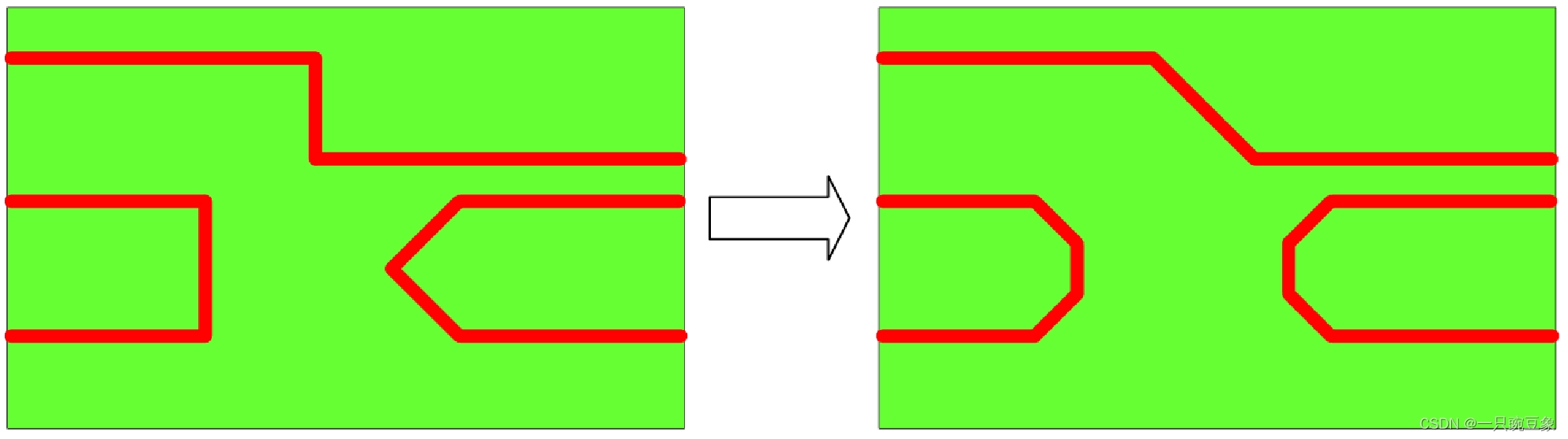
Avoid right-angle bends. Use 45° angles or curved bends. Right angles create small impedance discontinuities that matter above 5 GHz.
Never run RF and digital traces in parallel. Parallel traces couple. Even 5–10 mm of parallel routing at high frequencies creates measurable crosstalk.
Route RF signals on outer layers where possible. This simplifies impedance control, reduces the need for via transitions, and makes probing easier during debug.
Maintain a minimum 3× trace-width spacing between RF traces and any non-RF signals for frequencies above 1 GHz.
Ground Plane Integrity: The Rule Most Designers Break
Ground plane integrity is not a secondary concern. It is part of the transmission line itself.
Every RF microstrip trace has a reference plane directly beneath it. Splits, slots, or voids in that plane change the local impedance of the trace. This is one of the most common — and hardest to debug — RF layout errors.
Ground plane rules:
- No splits or slots under any RF trace.
- Stitch vias around RF sections at a spacing of λ/20 or less at the highest operating frequency.
- Add via fences on both sides of long RF traces to suppress surface-wave coupling between sections.
Decoupling Strategy for RF Circuits
Decoupling in RF is not just noise suppression. It prevents the power rail from acting as a coupling path between stages.
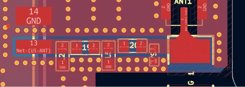
Place decoupling capacitors within 0.5 mm of each IC power pin for frequencies above 2 GHz. Use multiple values in parallel — e.g., 100 nF and 10 pF — to cover a wider frequency range. The smaller capacitor handles RF-frequency noise; the larger handles lower-frequency ripple.
For PA stages, add a ferrite bead in series with the supply line, then place a bulk capacitor before the bead and a small decoupling capacitor after it. This creates a two-stage filter that isolates the PA supply from the rest of the board.
With these layout decisions in place, the next question is how the layer structure supports them.
Stack-Up Design for RF PCBs: Matching Layers to Performance
Stack-up decisions determine impedance, insertion loss, stage isolation, and thermal management — all before the first trace is routed. Getting this right early prevents costly board respins.
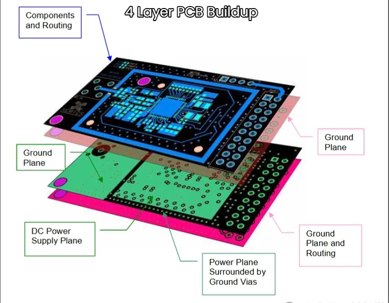
RF PCB stack-up design assigns signal, ground, and power layers to support controlled impedance, EMI shielding, and thermal dissipation. For most RF PCBs, 4-layer and 6-layer configurations are the most practical starting points, with 8+ layers for complex RF front-end modules.
Typical RF PCB Stack-Up Configurations
| Layer Count | Common Use Case | Typical Layer Configuration |
|---|---|---|
| 2-layer | Simple modules, sub-1 GHz | Signal / Ground |
| 4-layer | Most RF designs up to 6 GHz | Signal / GND / PWR / Signal |
| 6-layer | Multi-band, LTE/5G sub-6G modules | Signal / GND / Signal / GND / PWR / Signal |
| 8-layer | Phased array, radar front-end | Alternating signal-GND, RF + digital isolation |
| 10–12 layer | Complex RF SoC integration | RF front-end + digital backend, power islands |
Why 4-Layer Is the Minimum for Most RF Designs
A 2-layer RF board places the RF trace and its ground reference on opposite faces of the full board thickness — typically 1.6 mm. At that reference distance, maintaining 50 Ω microstrip requires very wide traces or impractically thin substrates.
A 4-layer board places a solid ground plane directly beneath the top signal layer. The core thickness between them can be 0.1–0.2 mm. This gives you narrow, well-controlled 50 Ω traces and a tight, consistent reference plane.
For RF PCBs above 2 GHz, 4-layer is the practical minimum. For designs that combine high-speed digital with RF, 6-layer provides the isolation needed to prevent digital switching noise from coupling into the RF ground structure.
From Layout to Manufacturing-Ready Files: What “Ready” Actually Means
Sending your PCB layout files to a manufacturer is not the same as sending manufacturing-ready files. The gap between the two is where most first-time RF board orders go wrong.
Manufacturing-ready RF PCB files include more than Gerber files. They must specify the stack-up, controlled impedance targets, material, surface finish, copper weight, minimum trace and space, drill files, netlist, and any RF-specific requirements. An incomplete package delays production, increases non-conformance risk, and makes it impossible for the manufacturer to verify your design intent.
The Minimum File Package for RF PCB Manufacturing
| File or Document | Purpose |
|---|---|
| Gerber files (RS-274X) or ODB++ | Layer geometry — copper, solder mask, silkscreen |
| Drill file (Excellon format) | Via and through-hole drill locations and sizes |
| Stack-up specification | Layer order, material, thickness, copper weight per layer |
| Impedance table | Target impedance, trace width, layer reference, tolerance |
| Fabrication drawing (PDF) | Board outline, drill legend, notes, surface finish specs |
| Netlist (IPC-356A) | For electrical continuity testing after fabrication |
| BOM + CPL file (for PCBA orders) | Component sourcing and pick-and-place guidance |
What RF-Specific Notes Must Appear on Your Fabrication Drawing
Standard PCB notes are not enough for RF boards. Your fabrication drawing must also include:
- Material specification: e.g., “Rogers RO4350B, Dk 3.48 ± 0.05.”
- Controlled impedance note with coupon requirement: e.g., “50 Ω ±10% on Layer 1, verified by TDR coupon on panel”
- Surface finish specification: ENIG for flat, consistent mating surfaces; HASL is not suitable for fine-pitch RF pads
- Copper weight per layer: e.g., 1 oz outer, 0.5 oz inner
- Solder mask requirements for RF traces: Some RF transmission lines require no solder mask over the trace to avoid Dk loading
Missing any one of these forces your manufacturer to make assumptions. At RF frequencies, those assumptions can cost you a full board spin.
RF PCB Design for Manufacturing: Why RF Needs Tighter DFM Rules
Standard DFM rules keep boards manufacturable. RF DFM rules keep boards performant. The difference is significant — and most generic DFM checklists miss it entirely.
RF PCB DFM goes beyond the minimum trace width and annular ring. It includes via placement rules that prevent RF path discontinuities, pad geometry requirements that maintain impedance at connectors, panelization strategies that avoid mechanical stress near RF structures, and inspection requirements specific to RF laminate fabrication.
RF-Specific DFM Checks Your Manufacturer Should Perform
- Impedance-critical trace verification: Every RF trace on controlled-impedance layers must match the specified width within ±0.025 mm after etching.
- Via placement in RF paths: Uncompensated transition vias in 50 Ω paths add inductance — typically 0.3–1 nH — which shifts impedance and causes reflections. Compensated via pads or back-drilled vias are required for frequencies above 10 GHz.
- Pad geometry at RF connectors: SMA, MMCX, and U.FL pads must match the manufacturer’s land pattern exactly. Oversized pads introduce impedance discontinuities at the connector launch.
- Copper voids under RF components: Any void in the ground plane under an RF component — even from a thermal relief pattern — changes local impedance. Solid pad connections, not thermal reliefs, are required for RF ground pads.
- Solder mask clearance on RF traces: If your design requires open-trace microstrip for specific Dk reasons, this must be explicitly specified and DFM-checked.
Panelization and RF PCB Integrity
Panelization affects RF performance in ways that don’t apply to standard PCBs.
Breakaway tabs introduce mechanical stress at the board edge. If that stress cracks the laminate near a fine-line RF trace or a controlled-impedance structure, the board fails — even though the copper looks intact to the eye.
For RF laminates such as Rogers and Taconic, V-score panelization is generally preferred over routed tab-break methods because it reduces mechanical stress at the board edge. If your RF structures are close to the board edge, flag this explicitly to your manufacturer before panelization is planned.

Working with a RF PCB Manufacturer: What to Send and What to Expect
Overseas clients lose days in back-and-forth with PCB factories in China because the initial inquiry doesn’t contain enough information. Knowing what to send upfront cuts lead time significantly.
To get an accurate RF PCB quote from a Shenzhen manufacturer, you need more than a Gerber file. The manufacturer needs your stack-up, impedance requirements, material, quantity, surface finish, and any special RF requirements. The more complete your inquiry, the faster and more accurate the quote — and the fewer surprises in production.
What to Include in Your First Inquiry to an RF PCB Factory
| Information | Why It Matters |
|---|---|
| Layer count | Determines manufacturing complexity and base cost |
| Board size and quantity | Enables yield calculation and panelization planning |
| Material (e.g., Rogers RO4350B) | Not all factories stock or process RF laminates |
| Stack-up (core and prepreg thicknesses) | Critical for impedance validation before layout locks |
| Controlled impedance targets | Must be agreed before CAM and production |
| Surface finish (ENIG, HASL, OSP) | Directly affects RF connector and pad performance |
| Minimum trace and space | Required for DRC and capability check |
| Via types (through-hole, blind, buried) | Determines process complexity and cost tier |
| Assembly requirement (bare PCB or PCBA) | Enables full-service quoting |
What a Qualified RF PCB Manufacturer Does Before Production
A competent RF PCB manufacturer — not just a generic PCB factory — will:
- Review your stack-up against your impedance targets and flag any conflicts before layout is final.
- Run a full DFM check on your Gerber files and report issues with suggested corrections.
- Confirm material availability and lead time for the specified RF laminate.
- Propose impedance test coupons on the production panel for TDR verification.
- Confirm surface finish compatibility with your RF connectors and package requirements.
At IWDF Solutions, we perform all of these as standard steps in our RF PCB quoting process. We provide PCB design, PCB reverse engineering, RF PCB manufacturing, and full PCBA production services for overseas clients — with English-language support, NDA protection, and a single point of contact from quote to delivery.
If you have an existing RF PCB you want to clone, reproduce, or improve, we can work from bare boards, partial schematics, or images. Our PCB design and reverse engineering team handles the full path from initial analysis to manufacturing-ready output files.
Why the Manufacturer Should Be Involved Before the Final Layout?
RF PCB design is not a process that ends at “send to fab.” The physical manufacturing process — etching tolerances, laminate behavior, via formation, copper plating uniformity — directly affects signal performance.
The most reliable way to get an RF PCB right on the first board spin is to involve your manufacturer before routing is complete. Share your intended stack-up early, get confirmation of their controlled-impedance capability and tolerances, ask for their standard via models if vias appear in RF signal paths, and confirm that the specific RF laminate is in stock before your deadline.
This design-manufacture collaboration is how professional RF engineering teams reduce costly respins. It is also what separates a one-stop PCB partner from a generic board house that only processes files.
Conclusion
RF PCB design is precise but not unpredictable. Every key decision — material, stack-up, impedance target, layout strategy, and DFM rules — follows a clear logic that flows from the RF system’s frequency, power, and performance requirements. That logic extends from layout choices to how the board is fabricated.
The most expensive mistake in RF PCB design is treating fabrication as a black box. Your manufacturer is part of the signal chain. Choose one that understands RF — not just PCB.
If you are designing an RF PCB for the first time, scaling from prototype to volume production, or need to reproduce or improve an existing RF board, IWDF Solutions offers end-to-end support: RF PCB design, PCB reverse engineering, RF laminate manufacturing, and full PCBA assembly — all under one roof in Shenzhen. Send us your requirements and we will respond with a detailed technical review and quote within 24 hours.
Frequently Asked Questions
Q: What frequency range qualifies as an RF PCB?
RF PCBs typically operate between 500 MHz and 100 GHz. Below 500 MHz, standard PCB design rules are often sufficient. Above 500 MHz, controlled impedance, material selection, and layout strategy all become critical to board performance.
Q: Can I use FR4 for my RF PCB design?
FR4 works for some applications below 1 GHz, particularly where performance requirements are not tight. Above 1–2 GHz, FR4’s dielectric loss (Df 0.020–0.025) causes measurable signal attenuation, and its inconsistent Dk makes impedance control unreliable. For most RF designs above 1 GHz, Rogers or PTFE-based laminates are the practical choice.
Q: What is controlled impedance and why does it matter for RF PCBs?
Controlled impedance means manufacturing the trace width, substrate thickness, and material properties to hit a specific electrical impedance — typically 50 Ω in RF systems. When impedance is not controlled, signal reflections occur at every mismatch point. Those reflections cause power loss, noise, and in some cases complete signal failure. For RF PCBs, controlled impedance is not optional — it is a core manufacturing requirement.
Q: How many layers does an RF PCB typically need?
Most RF designs above 2 GHz require at least 4 layers. The minimum configuration places a solid ground plane directly beneath the RF signal layer to enable tight impedance control. Designs combining RF with digital circuitry typically use 6 layers or more, to maintain isolation between domains.
Q: What files should I send to an RF PCB manufacturer?
At minimum: Gerber files or ODB++, Excellon drill files, a stack-up specification, an impedance table, and a fabrication drawing with material, surface finish, copper weight, and controlled impedance notes. For PCBA orders, add a BOM and component placement (CPL) file. Sending incomplete files is the most common cause of production delays and quoting errors.
Q: What is the difference between RF PCB design and PCB reverse engineering for RF boards?
RF PCB design starts from a schematic or system requirement and produces layout files for manufacturing. RF PCB reverse engineering starts from an existing board — with or without documentation — and reconstructs the schematic, layout, and bill of materials. Both require deep RF knowledge. At IWDF Solutions, we handle both services, including cloning and improving existing RF PCBs for clients who need to reproduce legacy hardware or optimize a competitor’s design.
Q: How do I choose between ENIG and HASL surface finish for my RF PCB?
ENIG (Electroless Nickel Immersion Gold) is the standard for RF PCBs. It provides a flat, consistent surface that preserves connector and pad geometry at RF frequencies. HASL leaves an uneven surface that introduces small impedance variations at connector launches and fine-pitch pads — a problem that gets worse as frequency increases. For any RF design above 1 GHz, specify ENIG.
Q: Why does via placement matter so much in RF PCB design?
A via in an RF signal path introduces parasitic inductance — typically 0.3 to 1 nH depending on via geometry. At RF frequencies, that inductance creates an impedance bump that reflects signal energy. For designs below 6 GHz, a single via in a well-designed 50 Ω path is manageable with careful pad compensation. Above 10 GHz, back-drilled vias or specialized RF via structures are required to maintain signal integrity through layer transitions.
Q: Can IWDF Solutions handle both RF PCB design and manufacturing as a single service?
Yes. IWDF Solutions provides a complete one-stop service: RF PCB design from schematic or system specification, PCB reverse engineering for existing RF boards, RF PCB manufacturing with controlled impedance and RF laminate support, and full PCBA production including SMT assembly and testing. Overseas clients can submit a single inquiry and receive design, fabrication, and assembly under one project.

