

Most PCB defects are invisible to the naked eye. Each test method catches a different category of failure — and no single test catches all of them.
PCB testing is not a single checkpoint at the end of production. Professional manufacturers apply a layered sequence of methods — SPI, AOI, X-ray, ICT, flying probe, FCT, JTAG, and burn-in — each targeting a different defect type at a different production stage. The right combination depends on your board’s complexity, your production volume, and how much a field failure actually costs you.
Many hardware teams focus on unit price when evaluating PCB suppliers. But the more important question is whether the supplier’s testing architecture matches the real risk profile of the board. A missing test stage does not show up in the quote — it shows up in the field. This article covers every major PCB test method: what it catches, what it misses, and how to decide what your project actually needs.

The Full PCB Testing Sequence: From First Print to Final Shipment
Most PCB defects do not appear in one place. They come from different stages of production — the paste print, the placement, the reflow, the assembly, and the firmware load. That is why a single test at the end of the line misses most of them.
A professional PCB test strategy is a sequence, not a checklist. Each method covers what the previous one cannot. Together, they create overlapping coverage that catches defects at the earliest, cheapest point in the process — before the cost of correction multiplies.
The table below shows all nine testing stages, in the order they are applied in a professional PCBA production line, and what each one is responsible for catching.
| Stage | Method | When Applied | Primary Target Defects |
|---|---|---|---|
| 1 | SPI — Solder Paste Inspection | After stencil printing, before placement | Paste volume, alignment, bridging |
| 2 | AOI — Automated Optical Inspection | After placement; after reflow | Missing parts, bridges, polarity, lifted leads |
| 3 | AXI — Automated X-Ray Inspection | After reflow | BGA voids, hidden joints, inner-layer defects |
| 4 | ICT — In-Circuit Testing | After reflow (with bed-of-nails fixture) | Wrong component values, shorts, opens |
| 5 | Flying Probe Testing | After reflow (no fixture) | Continuity, shorts, opens — for low volume / NPI |
| 6 | FCT — Functional Circuit Testing | Final stage, board powered | Firmware, interfaces, system-level function |
| 7 | JTAG / Boundary Scan | After assembly | IC-to-IC interconnects, BGA pins, in-system programming |
| 8 | Burn-in / ESS | Final stage, extended stress | Infant mortality, latent defects, thermal failures |
| 9 | Impedance / TDR Testing | During bare board fabrication | Controlled impedance, signal integrity |
The cost logic behind this sequence is straightforward. A paste defect caught before component placement costs almost nothing to fix — wipe the board and reprint. The same defect found after reflow costs ten to fifty times more in rework labor. Found as a field return after shipment, it costs hundreds of times more when logistics, warranty, and customer impact are included. Every stage in this sequence exists to intercept defects before they reach the next, more expensive stage.
Each method below is covered in the order it appears in the production line — what it does, what it cannot do, and how to decide whether it belongs in your testing plan.
Stage 1 — Solder Paste Inspection (SPI): Catching Defects Before They’re Baked In
Solder Paste Inspection (SPI) scans every pad on the board right after paste printing, before any component is placed. It measures paste volume, height, area, and alignment on each pad using 3D optical scanning — and flags any pad that falls outside tolerance before the board moves forward.
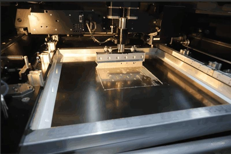
What SPI Measures — and Why 3D Matters?
Solder paste printing is a 3D process. A deposit can look perfectly normal from above and still be 30% under-volume — not enough material to form a reliable joint after reflow. A 2D camera sees shape and position. It cannot measure height or volume. That is why 3D SPI is the standard, not 2D.
The machine checks four parameters on every pad:
- Volume — is there enough paste to form a complete solder joint after reflow?
- Height — is the deposit within the acceptable thickness range for the stencil aperture?
- Area — does the deposit cover the pad correctly without spreading onto adjacent pads?
- Alignment — is the paste centered on the pad, or has it shifted toward an edge?
Each parameter has a defined pass/fail tolerance. A board is only released to the pick-and-place machine when every pad meets all four.
| SPI Defect Type | Root Cause | Risk If Missed |
|---|---|---|
| Insufficient paste volume | Clogged stencil aperture | Open circuit, cold joint |
| Excessive paste volume | Worn stencil, high squeegee pressure | Solder bridge, short circuit |
| Paste misalignment relative to pad center | Stencil registration error | Bridging, tombstoning |
| Paste slumping or shape deformation | Low-viscosity paste, elevated ambient temperature | Shorts on fine-pitch pads |
| Stencil clogging or partial blockages | Paste drying in aperture, insufficient cleaning | Starved joints on repeated boards |
| Bridging between adjacent pads | Pads too close, over-deposit, stencil wear | Short circuit after reflow |
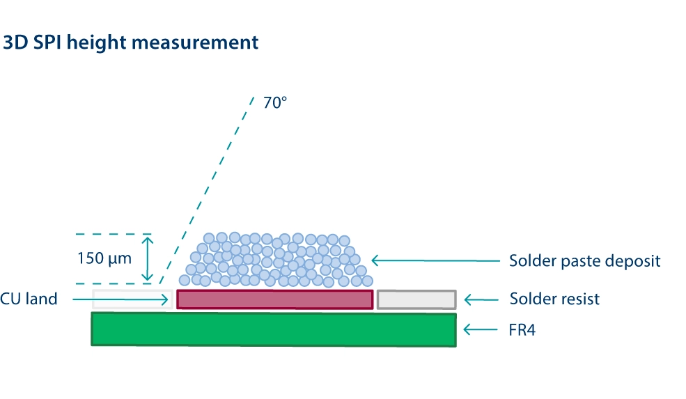
Why Inline SPI Beats Offline Sampling?
Some factories inspect paste manually or check one board offline after printing. That approach misses the real value of SPI. Inline 3D SPI feeds results back to the stencil printer in real time. When paste volume drifts low, the system signals the printer to adjust squeegee pressure, print speed, or cleaning frequency — before the next board runs. An offline sample check tells you something went wrong. An inline system stops it from repeating.
For boards with 0.4 mm pitch BGAs, 01005 passives, or fine-pitch QFNs, 3D SPI is not optional. It is the baseline.
With paste quality confirmed and components placed, everything goes through reflow. The next question is: once all joints are formed, how do you verify every component landed correctly and every joint holds?
Stage 2 — Automated Optical Inspection (AOI): Scanning Every Joint the Moment Reflow Is Done
After reflow, hundreds of components sit on a board. Manually checking every solder joint is impossible at production speed. But 2D and 3D AOI systems catch very different defects — and choosing the wrong type leaves real problems undetected.
Automated Optical Inspection (AOI) uses cameras and image processing to scan every component and solder joint after reflow. A 2D AOI detects obvious surface defects like missing parts, polarity errors, and severe bridges. A 3D AOI adds height measurement and catches lifted leads, insufficient solder volume, and component tilt — defects that are completely invisible in a flat image.
2D AOI vs. 3D AOI: What the Difference Means in Practice
| Feature | 2D AOI | 3D AOI |
|---|---|---|
| Imaging method | Single top-down camera | Structured light + multiple camera angles |
| Height measurement | No | Yes |
| Catches lifted leads | No | Yes |
| Catches solder volume deficiency | No | Yes |
| False call rate | Higher (shadows create false alarms) | Lower |
| Best for | Simple, low-density boards | Fine-pitch, high-density, mixed SMD |
A 2D system looks at the board from above. It sees shape, color, and contrast. It has no idea whether a component is tilted 5 degrees or a solder joint is 40% under-volume. Both look fine from above. Both cause field failures.

Where is AOI Deployed in a Professional SMT Line?
AOI is not only an end-of-line check. A well-run SMT line uses it at three points:
- Post-solder paste printing — as a complement to SPI on high-density boards
- Post-component placement — before reflow, while correction is still easy and cheap
- Post-reflow — the primary gate for verifying every solder joint
The One Thing AOI Cannot Do
AOI inspects surfaces. It cannot see through a component body to the pads underneath. BGA balls, QFN thermal pads, and any bottom-side solder joint are physically invisible to every optical system. For those connections, a different technology is needed — one that uses X-rays rather than light.
Stage 3 — Automated X-Ray Inspection (AXI): Seeing the Joints No Camera Can Reach
AOI is great for checking the surface, but it has a major blind spot: it can’t see what’s happening underneath a BGA. Since BGA packages sit flush against the board, the solder balls are completely hidden from view. Once they go through reflow, those joints are physically off-limits to any camera—and no amount of surface checking will tell you if they actually formed correctly.
To get a real answer, you have to look through the board. This is where Automated X-Ray Inspection (AXI) comes in. By using X-ray penetration, it images hidden solder joints under BGA, QFN, and CSP packages, even revealing internal structures in multilayer designs. It catches voids, cold joints, and bridges that optical tools simply miss. If your board uses BGAs, AXI isn’t just an option; it’s the only reliable, non-destructive way to verify the assembly
What X-Ray Inspection Detects That AOI Cannot?
At the PCBA level, X-ray inspection targets:
- BGA solder ball voids — IPC-A-610 Class 2 typically limits voids to less than 25% of joint cross-sectional area
- Cold joints or incomplete reflow beneath QFN thermal pads
- Solder bridges between adjacent BGA balls hidden below the package
- Ball collapse or tombstoning beneath package bodies
- Pin-in-paste defects on bottom-side assemblies
At the bare board level, X-ray also checks inner-layer copper delamination on multilayer boards, via fill quality for HDI constructions, and core registration in complex stack-ups.
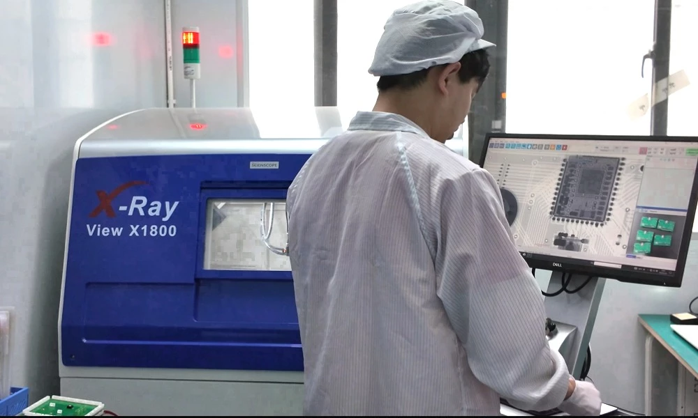
2D X-Ray vs. 3D CT X-Ray
| Feature | 2D X-Ray | 3D CT X-Ray |
|---|---|---|
| Image output | Flat projection | Full volumetric model |
| Overlapping layer handling | Difficult | Layer-by-layer analysis |
| Void measurement accuracy | Approximate | Precise percentage measurement |
| Suitable for | Standard BGA inspection | Medical, aerospace, automotive |
| Inspection speed | Fast | Slower |
For standard commercial boards, 2D X-ray catches the most critical BGA defects. For Class 3 applications — medical devices, aerospace electronics, automotive safety systems — 3D CT is the only way to measure void percentages accurately and inspect inner layers with confidence.
With surface inspection and hidden joint verification complete, the focus shifts to electrical: are all components functioning correctly, and are all nets properly connected?
Stage 4 — In-Circuit Testing (ICT): Verifying Every Component Value and Every Net Electrically
A board can pass every optical and X-ray check and still ship with the wrong resistor value, a reversed capacitor, or a net shorted by residual flux. ICT catches what no camera will ever find.
In-Circuit Testing (ICT) uses a bed-of-nails PCB test fixture to make simultaneous electrical contact with hundreds of test points across the assembled board. It measures resistor values, capacitor values, continuity, shorts, and basic semiconductor orientation. ICT catches approximately 90% of all assembly defects and is the highest-efficiency single electrical test available for medium-to-high volume production.
How the Bed-of-Nails PCB Test Fixture Works?
The bed-of-nails fixture is a custom piece of tooling built for one specific PCB design. It contains spring-loaded pogo pins aligned precisely to the test point layout on the board. When the board loads and vacuum pulls it down, all pins contact their target pads simultaneously. The ICT system applies small voltages and currents to each node and measures the response. A wrong-value resistor fails. A reversed capacitor fails. A solder bridge between two nets fails. A typical test cycle takes about one minute per board.

PCB Test Fixture Cost vs. Production Volume
| Fixture Factor | Typical Range |
|---|---|
| Fixture development time | 2–4 weeks |
| Cost for a simple board | $500 – $1,500 |
| Cost for a complex board | $2,000 – $5,000+ |
| Per-board test time | ~1 minute |
| Volume that justifies the cost | 300–500 boards minimum |
For a 50-board prototype run, paying $3,000 for a fixture to test $4,000 worth of boards does not make sense. For a 5,000-board production run, that same fixture costs $0.60 per board — a fraction of what one rework incident costs.
What ICT Cannot Test?
ICT verifies individual components and net connectivity with the board unpowered. It does not run the firmware. A microcontroller that is correctly placed and soldered will pass ICT perfectly — even if it carries corrupted firmware or a fatal configuration error. That gap is where Functional Circuit Testing takes over.
For prototypes and low-volume orders where a custom fixture is not yet justified, there is an approach that delivers the same electrical coverage with no tooling cost at all.
Stage 5 — Flying Probe Testing: Full Electrical Coverage With No Fixture Cost
You need electrical coverage on a 150-board prototype run. A custom ICT fixture costs $2,500 and takes three weeks to build. There is a better option — and most professional factories offer it as standard.
Flying probe testing uses motorized probes that move under software control across the board surface, contacting test points one by one — no custom fixture required. It provides equivalent electrical coverage to ICT, testing continuity, shorts, resistance, and capacitance values. The trade-off is longer per-unit test time and higher per-unit cost at scale. For prototypes and low-to-mid volume production, it is the right call.
Flying Probe vs. ICT: When to Use Each
| Criteria | ICT (Bed-of-Nails) | Flying Probe |
|---|---|---|
| Fixture required | Yes — custom per board | No |
| Setup time | 2–4 weeks | 1–3 days |
| Per-unit test time | ~1 minute | 5–15 minutes |
| Per-unit cost at high volume | Low (fixture cost amortized) | Higher |
| Upfront tooling cost | $500–$5,000+ | None |
| Design change flexibility | Fixture must be rebuilt | Software program updated in days |
| Best suited for | 500+ boards, stable design | NPI, prototypes, under 500 boards |

Flying probe programs are generated directly from CAD data. When a design changes, the test program updates in days — not weeks. This makes it the natural choice during design iterations.
In a well-managed factory, the transition from flying probe to ICT happens automatically as volumes scale. The manufacturer identifies the crossover point, builds the fixture, and manages the change. The buyer does not need to track it.
Once electrical verification is complete, one question remains: does the board actually do what it is supposed to do when power is applied?
Stage 6 — Functional Circuit Testing (FCT): Confirming the Board Works Under Real Operating Conditions
ICT confirmed all components are present and correct. Flying probe confirmed all nets are connected. The board powers up — and nothing works. Something was missed that no probe-based method can catch.
Functional Circuit Testing (FCT) applies real operating power to the assembled PCBA, injects real-world input signals, and verifies that every subsystem responds correctly. It tests what ICT cannot: firmware execution, communication interfaces, sensor accuracy, power rail behavior, and full system functionality. FCT requires a custom functional PCB test fixture, developed together with the client’s engineering team.
What FCT Verifies in a Live Board?
FCT operates the board as if it is already inside its end product. A complete FCT sequence checks:
- Power rail voltages at startup and under load conditions
- Communication interfaces: UART, SPI, I2C, CAN, USB, Ethernet
- Firmware boot sequence and normal execution
- Sensor inputs and calibration accuracy
- Display, LED, relay, and actuator outputs
- Current draw under normal and peak operating conditions
- Signal timing between subsystems
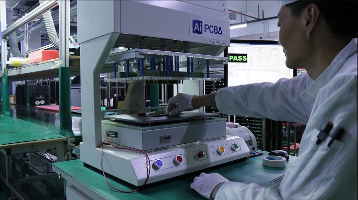
What the Functional Test Fixture Contains
The FCT fixture must replicate the board’s real operating environment. It contains a mechanical housing that holds the board in position, pogo pin contacts to key test points and connector interfaces, simulated loads matching the real application, and a host controller running the automated test sequence with defined pass/fail thresholds for every parameter.
Developing this fixture requires a test specification from the client — a document that defines what each subsystem must do and what a passing result looks like. Without that specification, no factory can build a meaningful FCT fixture. This is why professional manufacturers ask for a basic test spec during the PCB design phase, before production tooling is ever committed.
When IWDF Solutions handles a full design-to-production project, FCT fixture development begins in parallel with the PCB layout — not after the first batch fails.
Stage 7 — JTAG / Boundary Scan: Testing IC-to-IC Connections Without a Single Probe
Your board uses fine-pitch BGAs and dense FPGAs. Every critical net is buried beneath a package. ICT probes cannot make contact there. JTAG can test those connections without touching them.
JTAG boundary scan (IEEE 1149.1) tests IC-to-IC interconnects without any physical probe contact. It shifts test data through embedded scan cells inside compliant ICs to verify continuity on every pin of every JTAG-capable device — including BGA connections that sit beneath the package where no bed-of-nails can reach. It also supports in-system programming of FPGAs, CPLDs, and flash memory.
How Boundary Scan Works?
Every JTAG-compliant IC contains a daisy-chained register called the boundary scan chain. The test controller connects to the board through four signals — TDI, TDO, TCK, and TMS — at the Test Access Port (TAP). By shifting test patterns through this chain, the system drives signals onto board nets from inside the IC and captures results at adjacent IC pins. Opens and shorts between ICs are identified without placing a single probe on the board.
When JTAG Adds Real Value
| Board Characteristic | JTAG Value |
|---|---|
| High-density BGA ICs | High — BGA connections cannot be probed |
| FPGAs, CPLDs in the design | High — enables in-system programming |
| Mixed-signal or analog-dominant design | Low — JTAG is a digital test method |
| Simple, passives-heavy board | Low — coverage does not justify setup cost |
| More than 70% of ICs are JTAG-compliant | High — near-complete net coverage possible |
JTAG effectiveness depends entirely on decisions made during PCB layout. The TAP chain must be connected, JTAG-compliant ICs must be selected, and the TAP must be accessible at a header or test point. These choices cost nothing to implement during design. They cost a full board re-spin to add after production tooling is released.
With all assembly and connectivity tests complete, one final risk remains: a board that passed every production test but carries a hidden defect that only surfaces six weeks after delivery.
Stage 8 — Burn-In and ESS: Forcing Latent Defects to Surface Before the Board Ships
Every production test passed. The boards shipped. Four percent fail in the field within two months. The defects were there from day one — just invisible to every test that measures current performance rather than future reliability.
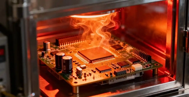
Burn-in and Environmental Stress Screening (ESS) run assembled boards under elevated electrical and thermal stress for 40 to 168 hours. The purpose is to force latent manufacturing defects to surface in a controlled environment before the board reaches the customer. This process eliminates “infant mortality” failures — defects present from production that only appear after weeks of normal use in the field.
The Four Main Burn-In Approaches
| Burn-In Type | What It Does | Primary Application |
|---|---|---|
| Static burn-in | Continuous DC bias at elevated temperature | Component-level screening |
| Dynamic burn-in | Full functional operation under thermal stress | System-level reliability validation |
| Thermal cycling | Rapid transitions between temperature extremes | Solder joint and via reliability |
| ESS (combined profile) | Temperature + humidity + vibration together | Aerospace, military, medical |
Thermal cycling is particularly relevant for multilayer boards with dense via structures. Every temperature cycle creates expansion and contraction stress in via barrels and solder joints. Cracks too small to detect by X-ray after assembly will grow under cycling and fail — in the chamber, before shipment, rather than at a customer site after deployment.
Burn-in is standard for medical devices, aerospace electronics, automotive safety systems, industrial automation controllers, and defense electronics. For consumer electronics, statistical sampling ESS is common — a defined percentage of each batch is screened rather than 100%.
Every stage covered so far tests the assembly — components, solder joints, firmware, and reliability under stress. None of them verify the electrical geometry of the bare board itself. A trace impedance that drifted during fabrication will pass all of them without triggering a single failure flag. That is what impedance and signal integrity testing is needs for.
Stage 9 — Impedance and Signal Integrity Testing: Making Sure High-Speed Signals Arrive Clean
A board can pass every assembly test and still fail in operation — because a trace impedance that is 15% off-spec turns a clean digital signal into a reflected noise problem that no ICT or FCT fixture will ever catch.
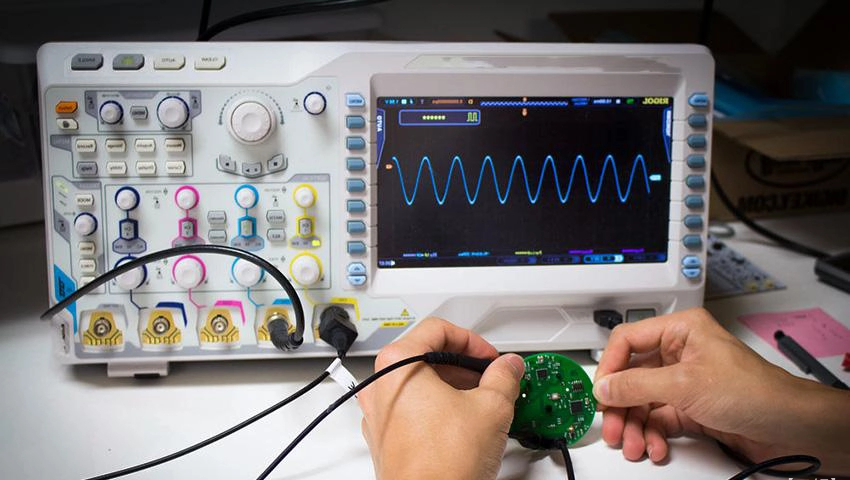
Impedance testing and signal integrity verification confirm that every high-speed trace on the board was fabricated to its designed electrical specification. For RF, 5G, high-speed digital, and controlled-impedance boards, this is not an optional quality step — it is a fabrication deliverable.
What Impedance Testing Covers?
Impedance testing is applied during bare board fabrication, before assembly begins. It uses Time Domain Reflectometry (TDR) to send a fast electrical pulse down a trace and measure how the signal reflects back. Any deviation between the designed impedance and the fabricated impedance shows up as a reflection — and the TDR system calculates the exact impedance value at every point along the trace.
Standard impedance targets are:
| Trace Type | Typical Target Impedance |
|---|---|
| Single-ended microstrip | 50 Ω |
| Single-ended stripline | 50 Ω |
| Differential pair (microstrip) | 100 Ω |
| Differential pair (stripline) | 100 Ω |
| RF / coplanar waveguide | 50 Ω (application-specific) |
The fabricated impedance is controlled by four variables: trace width, trace thickness, dielectric thickness, and dielectric constant (Dk) of the substrate material. All four are subject to manufacturing tolerance. A professional PCB manufacturer includes impedance test coupons — small test traces fabricated on the same panel as the production boards — and runs TDR on every panel before releasing boards to assembly.
What Signal Integrity Verification Adds?
Beyond impedance, high-speed boards require signal integrity verification at the system level. This includes:
- Eye diagram analysis: Confirms that serial data signals maintain clean transitions at operating speed — used for USB 3.x, PCIe, DDR, SERDES, and similar interfaces
- Jitter measurement: Quantifies timing uncertainty in high-speed clock and data signals
- Crosstalk measurement: Confirms that adjacent high-speed traces do not interfere with each other under real operating conditions
- Return loss and insertion loss: Standard measurements for RF and microwave boards, confirming signal transmission efficiency across the operating frequency range

When Impedance Testing Is Required?
| Board Type | Impedance Testing Required? |
|---|---|
| Standard digital board, speeds below 50 MHz | No |
| High-speed digital — USB, PCIe, DDR, SERDES | Yes — TDR coupon testing on every panel |
| RF and microwave boards | Yes — TDR + return/insertion loss |
| 5G and millimeter-wave boards | Yes — full signal integrity verification |
| Multilayer HDI with buried/blind vias | Yes — via impedance verification |
| Medical or industrial boards with high-speed data interfaces | Yes |
For every controlled-impedance order at IWDF Solutions, TDR coupon testing is included in the fabrication process and TDR test reports are delivered with the boards. For RF and 5G designs, our engineering team reviews the stack-up and trace geometry during DFM to confirm that the fabricated impedance will meet the design specification before a single panel is run.
Now that all nine testing stages are clear, the practical question becomes: how do you match this sequence correctly to your specific project — and how do you tell whether a supplier actually applies it?
How Do You Match the Testing Strategy to Your Specific Project?
Every manufacturer says they do “full testing.” What that covers varies from a final visual check to a complete ICT, FCT, and burn-in protocol. Knowing how to align the test stack to your board’s real risk profile is where cost and coverage decisions get made.
The right PCB testing strategy depends on three variables: production volume, board complexity, and application risk class. Prototypes need different coverage than high-volume production. BGA-heavy boards require X-ray that simple resistor-capacitor boards do not. Medical and industrial boards require burn-in that a consumer product can skip. Applying the same tests to every project either wastes money on unnecessary steps or under-protects where it actually matters.
Testing Method Selection by Volume and Application Class
| Testing Method | Prototype / NPI | Mid-Volume 500–5,000 | High-Volume 5,000+ | Class 3 / High-Reliability |
|---|---|---|---|---|
| SPI (3D) | Recommended | Standard | Mandatory | Mandatory |
| AOI (3D) | Standard | Standard | Standard | Mandatory |
| AXI (X-ray) | BGA boards only | BGA boards | Standard | Mandatory |
| Flying Probe | Standard | Optional | Rarely | Selective |
| ICT | Optional | Recommended | Standard | Standard |
| FCT | Recommended | Standard | Standard | Mandatory |
| JTAG | If design supports | Dense digital | Standard | Standard |
| Burn-in / ESS | Selected projects | Selected | Statistical | 100% mandatory |
| Impedance / TDR | If spec’d | If spec’d | If spec’d | Mandatory |
Design for Testability: The Upstream Decision That Controls Everything Downstream
Test coverage is limited by how testable the board was designed to be. A board that reaches the production line without adequate test point coverage, accessible probe pads, or JTAG-capable ICs creates hard limits on what any testing strategy can achieve — regardless of the equipment used.
Core DFT requirements to plan for during PCB layout:
- Test pad size: Minimum 1.0 mm diameter pads on all critical nets for ICT probe contact
- Test pad pitch: Minimum 2.54 mm (100 mil) spacing for standard bed-of-nails fixtures
- Single-side placement: All test points on one board side to reduce fixture complexity and cost
- Net coverage: Every net needs at least one accessible test point for 100% ICT coverage
- JTAG accessibility: TAP chain connected and accessible at a dedicated test header or pad
Every one of these decisions costs nothing to implement during layout. Every one costs a board re-spin to fix after production tooling is released. This is why DFT review belongs at the schematic stage — not the factory floor.
Knowing what a good test strategy looks like internally is one thing. Knowing how to evaluate whether a supplier actually applies it is another.
What Should You Ask a PCB Manufacturer About Their Testing Before You Send Files?
Most PCB suppliers list “testing” as a capability. What that means in practice ranges from a visual inspection station to a fully automated ICT and FCT production line. Asking vague questions gets vague answers. Specific technical questions reveal the gap fast.
The difference between a professional PCB manufacturer and a low-cost assembler is almost always visible in the specifics of their testing infrastructure — the machines they own, the protocols they follow in-house, and whether they can quantify their test coverage. Any supplier that responds to detailed technical questions with general reassurances about “quality commitment” is telling you something important.
The Ten Questions That Separate Professional Manufacturers from the Rest
- Is your SPI 3D or 2D, and is it deployed inline after every print cycle?
A supplier that uses 2D SPI or samples boards offline has a measurable blind spot on fine-pitch and BGA assemblies. - Is your AOI 3D, and is it deployed post-reflow for every board — not just on sample runs?
Post-reflow 3D AOI is the minimum standard for modern SMD assemblies. - Do you have in-house AXI? What is the machine’s resolution, and do you offer 3D CT X-ray?
A supplier that outsources X-ray cannot turn around rework decisions quickly and cannot guarantee 100% BGA joint coverage. - Can you fabricate ICT fixtures in-house, or do you outsource fixture manufacturing?
In-house fixture fabrication means faster turnaround and tighter iteration cycles when a board design changes. - What is your FCT fixture development process? Do you require a client-supplied test spec, or do you support joint development?
A manufacturer that cannot co-develop a test specification has limited system-level engineering capability. - Do you offer flying probe testing for prototypes with no MOQ requirement on the testing step?
This confirms whether their flying probe service is genuinely available or listed only as a marketing item. - What IPC-A-610 class do you certify production to, and is a test report included with each delivery?
Certified Class 2 or Class 3 with included inspection reports indicates a structured QMS — not informal checking. - Is a DFT review included in your pre-production DFM process, or is it a separate paid service?
Factories that review for testability before releasing to production catch problems early. Those that skip it pass the cost to you later. - For controlled impedance boards, do you include TDR coupon testing in the fabrication price, and do you deliver TDR reports with the boards?
This is a basic requirement for any RF, high-speed digital, or 5G-related board. - What certifications does your factory hold — ISO 9001, ISO 13485, IATF 16949, UL, RoHS, REACH?
Certification scope directly determines which regulated markets the boards can enter and which clients the factory is audited to serve.
A manufacturer that answers every one of these questions with specifics — machine models, turnaround times, coverage percentages — has built a testing infrastructure that is real. One that answers with generalities has not.
At IWDF Solutions, our testing infrastructure covers every method in this article — 3D SPI, 3D AOI, in-house AXI, ICT with in-house fixture fabrication, flying probe for NPI batches, FCT with co-developed test fixtures, JTAG integration, burn-in, and TDR impedance coupon testing. DFM and DFT review are part of every pre-production process, not an add-on. For clients bringing boards without existing test documentation, our engineering team builds the testing architecture from scratch — including fixture design, test specification development, and burn-in protocols matched to the application class. Contact us to start a pre-production consultation.
Frequently Asked Questions
What is PCB testing?
PCB testing is the process of inspecting and electrically verifying a printed circuit board or assembled PCBA to confirm it is free of manufacturing defects and functions correctly. It covers both inspection methods (SPI, AOI, AXI) and electrical test methods (ICT, flying probe, FCT, JTAG, burn-in), applied at different stages of the production process.
What is the most common PCB testing method used in production?
AOI (Automated Optical Inspection) is the most widely deployed PCB testing method. It is used across virtually all SMT production lines to verify component placement and solder joint quality after reflow. For electrical verification, ICT is the most common method at medium-to-high volume, and flying probe testing is the standard for prototypes and NPI boards where no fixture investment is justified yet.
What is a PCB test fixture and why does it matter?
A PCB test fixture is a piece of custom tooling — typically a bed-of-nails fixture for ICT or a functional housing for FCT — that makes repeatable mechanical and electrical contact with a specific board design during testing. The quality of the fixture directly determines test coverage and reliability. Poorly designed fixtures produce false failures and missed defects. In-house fixture fabrication gives manufacturers more control over both quality and turnaround time than outsourced tooling does.
What is the difference between ICT and functional testing?
ICT tests individual component values and net connectivity with the board unpowered. It confirms every component is present, correctly placed, and within specification. Functional Circuit Testing (FCT) powers the board and verifies that all subsystems work together as designed — including firmware, communication interfaces, and sensor behavior. ICT cannot catch firmware errors. FCT cannot measure individual component values. Both are needed for a complete test strategy on any board with digital logic or communication interfaces.
When should I use flying probe testing instead of ICT?
Flying probe testing is the right choice for prototype runs, NPI boards, and production volumes below approximately 500 boards where the cost of building a custom ICT fixture is not yet justified. It provides equivalent electrical coverage to ICT with no upfront tooling cost, and test programs can be updated in days when a design changes. For stable designs at higher volumes, ICT provides faster throughput and lower per-unit testing cost.
Can AOI replace X-ray inspection for BGA boards?
No. AOI inspects surfaces using optical cameras. BGA solder balls sit beneath the package body and are physically inaccessible to any camera. AOI provides zero coverage of BGA solder joint quality. For any board that uses BGA, QFN, CSP, or any bottom-side hidden package, AXI (Automated X-Ray Inspection) is the only non-destructive method that can verify solder joint integrity beneath those packages.
What does IPC-A-610 Class 2 vs. Class 3 mean for my boards?
IPC-A-610 is the global standard for acceptable electronic assembly quality. Class 2 covers dedicated-service products where reliable performance is expected — industrial controls, telecom equipment, and most commercial electronics. Class 3 covers high-performance products where downtime or failure is not acceptable — medical devices, aerospace electronics, military systems, and automotive safety controls. Class 3 applies tighter tolerances for solder joints, BGA void percentages, cleanliness, and component placement. Specifying your required IPC class at order stage ensures all inspection and testing thresholds are calibrated correctly from the start.
What is Design for Testability (DFT) and why does it affect production cost?
Design for Testability (DFT) is the practice of designing a PCB so that every net can be electrically accessed during production testing. It includes placing test pads of adequate size, routing them to accessible locations, connecting JTAG chains, and providing power and ground access for FCT. A board designed without DFT may have entire sections that cannot be tested, or require expensive fixture workarounds. A 30-minute DFT review during layout can eliminate thousands of dollars in rework costs or board re-spins later.
What burn-in testing duration is standard for industrial PCBAs?
For industrial PCBAs, dynamic burn-in typically runs for 48 to 96 hours at elevated temperature, with the board operating under normal functional conditions. Thermal cycling protocols commonly specify 50 to 100 cycles between -40°C and +85°C. The specific duration and temperature profile are set by the application class and reliability target — a medical device targeting long MTBF will require a more demanding profile than a general industrial controller.
How do I evaluate a PCB manufacturer in China for testing quality?
Ask specific technical questions about each testing method rather than accepting general capability claims. Confirm whether SPI and AOI are 3D, whether X-ray is in-house, whether ICT fixtures are built internally, and whether FCT is co-developed with clients. Request a sample test report from a comparable past project. Verify certifications — ISO 9001 at minimum, ISO 13485 for medical, IATF 16949 for automotive. A manufacturer that answers every technical question with measurable specifics has built a real quality infrastructure. One that answers with assurances has not.

