
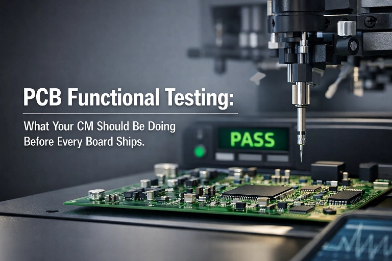
Shipping a PCB assembly means more than confirming it was built to spec. It means confirming it works — under real firmware, real load, and real operating conditions. That final confirmation is what PCB functional testing is responsible for.
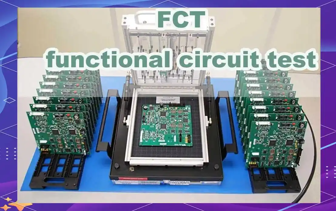
PCB functional testing (FCT) is the final, critical quality gate in PCB assembly. It powers the fully assembled board on and validates its real-world operating behavior — verifying power-on sequencing, firmware execution, every I/O response, and all communication interfaces — to detect design, assembly, and component defects before a single board leaves the production floor.
For buyers sourcing PCBA internationally, understanding what a rigorous FCT process looks like is one of the most practical tools available for evaluating a supplier before placing an order — not after receiving a field return. This article breaks down exactly what that process should include, step by step, at every production scale, so you know the right questions to ask and the right standards to hold your PCB CM to.
What Is PCB Functional Testing?
PCB functional testing (FCT) simulates the board’s real operating environment — applying power, loading firmware, and exercising every I/O path and communication interface — to validate that the assembled board behaves exactly as designed. It is the only test in the entire production sequence that detects defects invisible to every earlier inspection method: firmware issues, marginal components, signal integrity failures, and power sequencing violations that produce no visible physical defect.
Why “Assembled Correctly” and “Actually Works” Are Two Different Things?
The distinction sounds obvious. In practice, most production processes treat them as the same thing — and that gap is where field failures come from.
Every inspection method that runs before FCT measures something physical: the presence of a component, the continuity of a solder joint, the alignment of a pad. These methods answer one question: was the board built according to the design?
FCT answers a different question: Does the board do what it was designed to do?
A board can answer “yes” to the first question and “no” to the second. These are the failure types that make that possible:
- A firmware version was loaded that doesn’t match the hardware revision
- A component is correct-looking but has different internal timing behavior than the original
- A power rail reads correctly at the regulator output, but drops out of spec at the processor under load
- A communication interface transmits data but corrupts packets at the operating frequency due to a trace impedance problem
None of these produces a visible physical defect. None are detected by AOI, ICT, or X-ray. All of them cause product failures in the field.
A power-on check tells you the board draws current. FCT tells you the board works. These are not the same thing — and keeping this distinction in mind is what the rest of this article is built around.
How Is PCB Functional Testing Different from AOI, ICT, and Every Other PCB Test?
AOI, ICT, X-ray, and flying probe all inspect the physical assembly — component placement, solder joint quality, continuity, and component values. PCB functional testing verifies system-level behavior: whether all components, firmware, and interfaces work together as a functioning product. Each method in the testing stack has a specific role, and a professional CM uses all of them in sequence.
How Each Test Targets a Different Failure Mode
No single test catches everything. Each method is built for a specific failure category — and has specific blind spots. Understanding this is how you judge whether your CM’s process covers the right ground or leaves critical gaps.
| Test Method | What It Detects | When Applied | What It Cannot Catch |
|---|---|---|---|
| AOI | Missing parts, misalignment, polarity errors, solder bridges | Post-reflow | Wrong component values, firmware issues, signal integrity |
| AXI (X-Ray) | Hidden solder voids, BGA joint quality, internal shorts | Post-reflow, complex boards | System behavior, firmware, I/O response |
| ICT | Component values, shorts, opens, wrong parts | After full assembly | Firmware, power sequencing, communication behavior |
| Flying Probe | Same as ICT — no fixture required | NPI, prototypes, low volume | Same blind spots as ICT |
| Boundary Scan / JTAG | Interconnect integrity on high-density ICs | Complex digital boards | System-level analog behavior, power rail response under load |
| FCT (Functional Test) | Firmware, I/O, power rails, communications, system behavior | Final stage, before shipment | Structural defects — FCT complements, not replaces, earlier tests |
| Burn-In / ESS | Latent component failures, thermal stress failures | After FCT, high-reliability builds | Extends FCT coverage under stress — not a replacement for FCT |
FCT does not make earlier testing redundant. Each method covers ground the others cannot. A complete quality process uses all of them in sequence.
Where the Real Risk Lives
AOI and ICT are essential steps in any serious PCBA process. But their role ends at the component and assembly level. What neither method validates is system-level behavior — how the board performs when firmware is running, when all interfaces are active, and when power rails are operating under full load. FCT is the step in the production sequence that covers this ground. Without it, system-level behavior is only confirmed when the board reaches its end application — which is the most expensive place to find a problem.
The defects that survive AOI and ICT — wrong component values within tolerance, marginal solder joints, firmware-hardware mismatches, signal integrity failures at operating frequency — don’t produce visible damage. They produce functional failures: a board that boots intermittently, a communication interface that drops data under load, a power rail that sags at full current draw.
FCT is a standard part of any professional CM’s production process — applied consistently across production volumes, from low-volume NPI builds through high-volume runs. With the role of each test method in the full stack now clear, the next question is: what does a complete, layered pre-shipment testing process actually look like in practice?
What Does a Complete PCB Testing Stack Look Like Before Any Board Ships?
“We test every board” sounds reassuring. In practice, it can mean anything from a multi-stage automated verification process to a quick visual check. The difference shows up in your first field return.
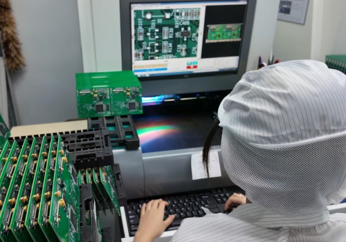
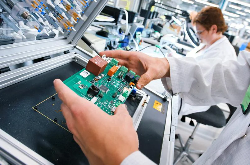
A complete pre-shipment PCB testing process layers multiple methods at defined stages: SPI post-paste printing, AOI post-reflow, AXI for BGA and complex boards, ICT or flying probe for component-level verification, and FCT as the final functional gate. Each stage catches a specific failure category. Skipping any layer leaves a specific blind spot — one your customer will eventually find.
The Full Pre-Shipment Quality Gate Sequence
| Stage | Method | What Gets Verified | Output |
|---|---|---|---|
| Pre-production | DFM / DFT review | Manufacturability, test point access, board testability | DFM/DFT report |
| Post-paste printing | SPI | Paste volume, deposit alignment, bridging risk | SPI data log |
| Post-reflow | AOI | Component presence, polarity, alignment, solder quality | AOI report |
| BGA / complex boards | AXI (X-ray) | Hidden joint integrity, void percentage, internal shorts | X-ray report |
| Low volume / NPI | Flying probe | Component values, shorts, opens at all accessible nets | Flying probe report |
| Medium–high volume | ICT | Component values, shorts, opens at fixture test points | ICT pass/fail log |
| All production | FCT | Firmware, I/O, power rails, communication interfaces | Per-board FCT log |
| High-reliability builds | Burn-in / ESS | Latent failures, thermal stress behavior | ESS certificate |
Why DFT Review at the Start Changes Everything
Most buyers think about testing at the end of a project. A professional CM thinks about it at the beginning.
DFT — Design for Testability — is a review of the board’s design before production begins, confirming that the board can actually be tested properly. This means verifying that test points are accessible, power rails can be independently probed, and net names in the design files match what the test software expects.
A DFT issue caught during the review stage costs almost nothing to fix. The same issue found mid-production means either a board re-spin or permanently reduced test coverage across the entire batch. Many buyers discover this only after it’s too late to change anything.
If your CM never asks about test points, never asks for a test specification, and never raises DFT before production begins — testing is an afterthought in their process, not an integrated engineering discipline.
With the full testing stack in view, the more immediate question becomes: what should each step within FCT specifically look like, in concrete terms?
What Should Your CM Do, Step by Step, During Every FCT Run?
A board that fails in the field rarely fails because of a single bad component. It fails because no one verified the complete system behavior before it shipped. Understanding what each FCT step covers — and why it exists — is how you evaluate whether your PCB CM’s process is thorough or superficial.
A complete FCT sequence covers six steps: test specification review, quiescent current check, power rail verification, thermal screening, firmware boot validation, and I/O stimulus-response testing. Each step targets a specific failure category and produces a logged result.
Step 1 — Test Specification Review
Before any board is connected to test equipment, the CM needs a test specification document (TSD). The TSD defines what a passing board looks like — in measurable terms — making every test step reproducible regardless of who runs it.
A complete TSD covers:
- Supply voltage and acceptable current range at each power rail
- Firmware version and programming interface (JTAG, SWD, UART, ISP)
- Input stimulus sequences and expected output responses
- Pass/fail threshold values for every measured parameter
- Communication interface behavior — packet format, timing windows, error handling
Tools used: Version-controlled engineering documents or test management software. On automated FCT lines, the TSD is translated directly into the test software configuration.
Step 2 — Quiescent Current Check
Before firmware boots, the board is powered on and its current draw is measured. Anything abnormal at this stage has a purely physical cause — a short circuit, a wrong component value, or a failed regulator — because no software is running yet. It is one of the cleanest diagnostic signals in the entire sequence and takes under 30 seconds.
Tools used: A programmable benchtop power supply with real-time current readout — such as the Keysight E36300 series or equivalent. On automated FCT lines, a source measure unit (SMU) is integrated into the test fixture and logs the quiescent current reading automatically before the boot sequence begins.
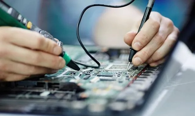
Step 3 — Power Rail Verification Under Load
Every power rail is measured at the processor — not at the regulator output. A regulator can produce the correct voltage at its output pin and still fail to deliver that voltage at the MCU under full operating current, due to trace resistance or insufficient copper in the power plane.
Tools used: A digital multimeter (DMM) with at least 4.5-digit resolution — such as the Fluke 87V or Keysight 34461A — for manual builds. On automated FCT fixtures, multiplexed voltage measurement modules log all rail readings simultaneously under defined load conditions.
Step 4 — Thermal Screening at Power-On
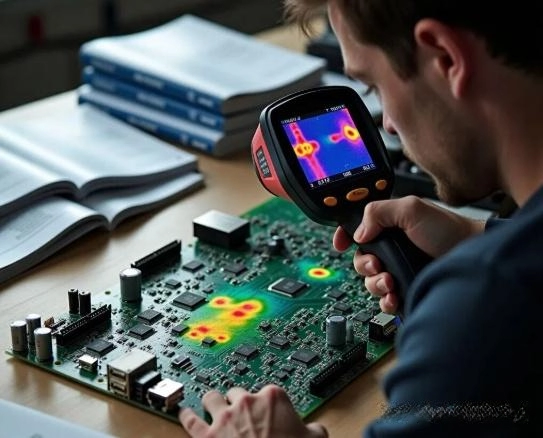
Within seconds of power-on, the board surface is scanned for heat anomalies. Any component drawing more current than expected generates a visible hot spot before any electrical anomaly appears at a probe point. On dense boards, this step locates the fault in seconds — without it, the same fault could take hours to isolate.
Tools used: A handheld IR thermometer for basic screening. For complex or dense boards, a thermal imaging camera — such as the FLIR E series — provides a full-board temperature map. Some high-volume FCT lines integrate a fixed overhead thermal camera that captures and compares each board against a reference thermal profile automatically.
Step 5 — Firmware Loading and Boot Validation
For any board with a programmable device — MCU, FPGA, or DSP — the CM loads production firmware from a version-controlled source and confirms correct boot behavior.
A complete boot validation confirms:
- Firmware loads without error through the correct programming interface
- Boot sequence completes within the defined time window
- The chip returns the correct device ID and memory map
- All peripheral drivers initialize without fault
- No watchdog reset loop or hung boot state occurs
Tools used: J-Link, ST-LINK, or ULINK for ARM-based MCUs; Xilinx Platform Cable or Intel USB Blaster for FPGAs. In production, gang programmers or in-fixture programming modules flash multiple boards simultaneously with firmware version verified and logged before testing proceeds.
Step 6 — I/O Stimulus-Response Testing and Edge-Condition Verification
Every I/O line, communication interface, and signal path is exercised against defined pass/fail thresholds — first under nominal conditions, then under stress conditions that expose marginal behavior.
Nominal condition testing covers:
- GPIO outputs driven and measured; GPIO inputs tested with controlled stimulus and verified response
- ADC inputs driven with a calibrated voltage reference; firmware readings compared against the known value
- DAC outputs measured against expected voltage
- All communication interfaces — UART, SPI, I2C, CAN, USB, RS-485, Ethernet — tested for correct framing, timing, CRC, and ACK behavior
- All sensor interfaces verified for correct communication and plausible output range
Edge-condition testing covers:
- Board operation at the low and high ends of the supply voltage range
- Clean recovery from a commanded reset and a full power cycle
- Firmware behavior when receiving a malformed packet
- Communication bus recovery from a timeout or contention event
Tools used: Protocol analyzers such as the Saleae Logic Pro or Total Phase Beagle for communication interface verification. Precision signal generators and calibrated voltage references for ADC and DAC validation. For automated production FCT, NI PXI or similar modular platforms integrate all stimulus and measurement functions into a single scripted sequence — controlled by NI TestStand, LabVIEW, or Python-based frameworks — with every result logged per board automatically.
Every result from every step is logged per board — serial number, firmware version, operator ID, timestamp, and every measured parameter value against its threshold. This record is the evidence that structured FCT was actually run — and the foundation for any failure investigation that follows.
Which Defects Does FCT Catch That Earlier Tests Completely Miss?
“Our AOI report is clean” is not a safety net. Several of the most common causes of field failure leave no physical trace — they are completely invisible to every inspection method that runs before FCT.
FCT routinely catches six categories of defects that survive AOI, ICT, and X-ray: wrong component values within tolerance, marginal solder joints that pass continuity checks but fail under thermal stress, firmware-hardware version mismatches, high-speed signal integrity failures, power sequencing violations, and BOM substitutions where the replacement part has a matching footprint but different internal behavior. None of these require a visible physical defect. All of them cause product failures in the field.
Six Defect Types That Are Invisible to Every Earlier Test
| Defect Type | Why Earlier Tests Miss It | How FCT Catches It |
|---|---|---|
| Wrong component value within tolerance | ICT passes if value is within ±5% or ±10%; circuit is still miscalibrated | Analog output doesn’t match the calculated expected value at the test threshold |
| Marginal cold solder joint | Passes ICT probe pressure; develops intermittent open under thermal expansion in operation | Fails during thermal edge-condition testing in the FCT sequence |
| Firmware-hardware version mismatch | AOI and ICT cannot read firmware version numbers or IC register maps | Board fails to boot, hangs in reset loop, or produces incorrect I/O response |
| High-speed signal integrity failure | Continuity test passes; signal degrades at operating frequency due to trace impedance mismatch | Protocol analyzer logs CRC errors, framing errors, or data dropouts during communication test |
| Power rail sequencing violation | ICT tests each rail independently; sequencing is a system-level behavior | Board fails to boot consistently or crashes intermittently on the FCT bench |
| BOM substitution with matching footprint | AOI sees a correct package; ICT sees normal continuity at all nodes | Firmware receives wrong register map, wrong timing response, or wrong output behavior |
A concrete example of how this plays out:
A 0402 ceramic capacitor on a power rail measures within 10% of its nominal value. ICT passes it. Under normal operating conditions — room temperature, low current draw — the circuit behaves correctly. At 60°C with full load current, the capacitor’s effective value drops significantly due to its DC bias characteristic. The downstream regulator becomes marginally stable. The processor resets intermittently.
AOI never flagged it. ICT never flagged it. The customer deploys 500 units. Six weeks later, field returns start arriving with “random resets” — one of the most difficult failure modes to diagnose, and one of the most expensive to handle in the field.
FCT’s edge-condition testing — specifically, rail behavior under full load at elevated temperature — catches this before a single board ships.
Each defect category in the table above has a specific FCT step that catches it, precisely because FCT looks at system behavior rather than assembly quality. With these failure modes understood, the practical question becomes: how does FCT actually scale across different production volumes?
How Should FCT Be Implemented Across Different Production Volumes?
FCT for a 5-board prototype looks nothing like FCT for 5,000 boards. If your CM describes the same testing process for both, one project is being shortchanged. It is almost always the high-volume run — where scale makes shortcuts feel economical and consequences are largest.
FCT scales with production volume. For prototypes and NPI, the process is engineering-led and focused on design verification and test specification development. For low-to-medium volume, semi-automated fixtures reduce operator variability. For high-volume production, full automation with integrated firmware flashing, scripted test sequences, and statistical process control (SPC) monitoring is the baseline standard.
FCT Implementation by Production Stage
| Production Stage | Typical Board Count | FCT Method | Key Deliverable |
|---|---|---|---|
| Prototype / NPI | 1–50 | Semi-manual, bench instruments, engineering bring-up | First-article inspection (FAI) report, DFT feedback |
| Low-to-medium volume | 50–500 | Semi-automated fixture, scripted test sequence | Per-board pass/fail log with parameter values |
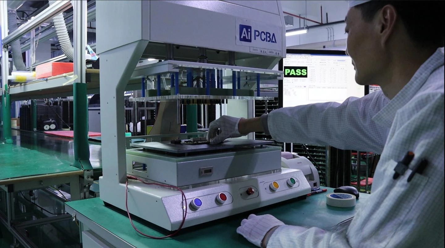
| High volume | 500+ | Automated bed-of-nails FCT, integrated firmware flashing, SPC monitoring | Full per-board test record database, yield trend data |
| High-reliability (any volume) | Any | FCT + burn-in / ESS thermal cycling | ESS pass certificate, time-to-failure data |
NPI Testing: Why the First Board Matters Most
At the prototype stage, the first assembled board should go through a first-article inspection (FAI) — a detailed, systematic validation of every measured parameter against the design specification.
The FAI report becomes the calibrated baseline for all production testing. Every parameter threshold in the production FCT setup is set from this document. If the FAI is skipped or done informally, production test thresholds are either guessed or copied from the design specification without being validated against actual assembled hardware. The gap between those two approaches is where false passes and false failures both come from.
NPI stage is also where DFT issues surface with the lowest cost to fix. A missing test point found during FAI can be added in the next layout revision with minimal impact on cost or schedule. Found during a 1,000-board production run, the same issue means accepting reduced test coverage or authorizing a re-spin with a production delay.
What Full Automation Actually Means at High Volume
At the production scale, manual FCT introduces operator-dependent variability that is both unacceptable and untraceable. A proper automated FCT setup includes:
- A custom bed-of-nails fixture built specifically for the board, making simultaneous contact with all test points in one operation
- Automated test software running a defined, version-controlled stimulus-response sequence
- Integrated firmware flashing within the test cycle — not a separate operation handled by a different operator
- Per-board data logging with serial number, firmware version, operator ID, and timestamp
- SPC monitoring on test yield data to detect process drift before it produces a systematic batch of failures
If your CM is doing manual power-on testing on a 1,000-board production run, the risk doesn’t disappear — it gets transferred to you.
What Are the Real Red Flags That Your CM Is Cutting Corners on PCB Testing?
Most CMs won’t say they skip functional testing. They describe testing in confident, reassuring language. The problem is almost always in the specifics — or the absence of them.
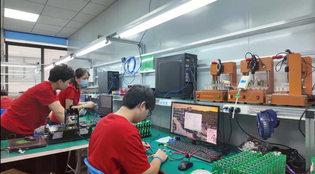
Five specific red flags signal that a CM’s testing process is inadequate: FCT is priced as an optional add-on; testing is described in vague terms; no per-board test records exist from previous projects; no DFT review is offered before production begins; and the same testing process is described for all production volumes regardless of scale.
Five Warning Signs That Deserve a Direct Conversation
Red flag 1: FCT is a line item you can remove from the quote
A CM that prices FCT as a removable line item has already told you what their default shipment standard is. When field returns come in — and they will — the cost of rework, replacement, and customer relationship repair will far exceed whatever the FCT line item was worth.
Red flag 2: Testing is described in phrases like “we check every board works.”
That is not a test procedure. A professional CM can name the specific parameters being tested, state the pass/fail threshold for each, describe how results are recorded, and tell you where that data is stored and for how long. Vague descriptions almost always reflect a vague process. Press for specifics. If the answers remain vague, that is the answer.
Red flag 3: No test records available from previous projects
Ask to see a sample test report from a recent build — customer data removed. If the CM cannot produce one, they either don’t keep structured records or don’t run structured testing. Without per-board records, you have no traceability when a field failure occurs and no basis for a warranty claim.
Red flag 4: DFT is never raised during the project kick-off
A CM with a mature testing process reviews the board for testability before production begins. If your CM never asks about test points, never requests a test specification, and never asks how the board should be connected during FCT — testing is not integrated into their engineering process. They are adding a check at the end of a line that was never designed with testing in mind.
Red flag 5: The same testing description applies to every project regardless of volume
A 10-board NPI build and a 2,000-board production run have fundamentally different testing requirements. A CM that describes one uniform process for all volumes is not adapting their approach to your actual project. Identify which volume category is being shortchanged before you commit.
Which Standards Should Your CM Reference for PCB Testing?
“We follow industry standards” is a claim that requires no evidence to make. The standards that actually govern PCB testing are specific and named — and a professional CM cites them without hesitation.
The key standards governing PCBA testing are IPC-A-610 (assembly workmanship and acceptance criteria for Classes 1 through 3), J-STD-001 (soldering process requirements), IPC-6012 (bare board electrical performance), IPC-9257 (electrical testing procedures for bare boards), and IPC-7711/7721 (rework and repair procedures after failed inspection). The IPC class your CM targets by default determines the workmanship standard applied to every joint, every test point, and every inspection step across your entire production run.
IPC Classes: What They Mean for Your Application
| IPC Class | Target Application | Workmanship Standard | Minimum Expected Test Coverage |
|---|---|---|---|
| Class 1 | Consumer electronics, general-purpose assemblies | Functional acceptability is the baseline | AOI + basic FCT |
| Class 2 | Industrial equipment, telecom, long-service products | Higher reliability, documented processes required | AOI + ICT or flying probe + FCT |
| Class 3 | Medical devices, aerospace, defense, automotive safety | Zero-defect criteria, full traceability, no acceptable compromises | Full stack: AOI + AXI + ICT + FCT + ESS burn-in |
When sourcing PCBA from China, always confirm which IPC class the CM defaults to before production begins. Many factories default to Class 1 unless a higher class is explicitly stated in the purchase order. Most international buyers assume Class 2 without confirming it. That assumption is where the majority of quality gaps start.
Specifying the IPC class in your purchase order is not paperwork. It is the most direct way to align your quality expectation with your CM’s production standard before a single component is placed.
Three questions to ask every CM on this topic:
- What IPC class does your production default to, and what do you require from us to produce Class 2 or Class 3?
- Are your IPC inspection and solder technicians certified in-house, or do you contract external audits?
- Can you provide IPC-A-610 inspection records on request for our production builds?
A CM with real IPC competence answers all three in specific terms without needing to check with a manager.
How Does IWDF Solutions Handle PCB Functional Testing Before Every Board Ships?
Knowing what good testing looks like is useful. Knowing that your specific CM executes it — with documented steps, verified equipment, and traceable records — is what matters when you are about to commit to a production order.
At IWDF Solutions, every PCBA build moves through a layered, documented quality process: from DFM/DFT review before production begins, through full FCT before shipment, with burn-in and ESS available for high-reliability applications. As described throughout this article, every board’s test result is logged per-board with full traceability — and that data is available to customers on request.
IWDF Solutions’ Standard PCBA Quality Gate Sequence
| Stage | Method | What We Verify | Documentation Output |
|---|---|---|---|
| Pre-production | DFM / DFT review | Manufacturability, test point access, board testability | DFM/DFT report provided to customer |
| Post-paste printing | SPI | Paste volume, deposit alignment, bridging risk | SPI data log |
| Post-reflow | AOI | Component presence, polarity, alignment, solder bridges | AOI report |
| BGA / complex boards | AXI (X-ray) | Hidden joint quality, void percentage, BGA integrity | X-ray inspection report |
| Low volume / NPI | Flying probe | Component values, shorts, opens at all net access points | Flying probe report |
| Medium–high volume | ICT | Component values, shorts, opens at fixture test points | ICT pass/fail log |
| All production | FCT | Firmware boot, I/O response, power rails under load, communications | Per-board FCT log with all parameter values |
| High-reliability builds | Burn-in / ESS | Latent failures, thermal stress behavior, marginal components | ESS pass certificate |
For customers who arrive without a test specification document, our engineering team develops one as part of the NPI engagement. This is an engineering task — not a form. It covers power rail thresholds, firmware version control, I/O stimulus-response sequences, communication interface behavior, and edge-condition pass/fail criteria.
We serve clients across industrial automation, medical devices, IoT, consumer electronics, telecommunications, and power systems — in North America, Europe, Australia, and Southeast Asia.
Our one-stop capability covers PCB design, PCB reverse engineering, bare board manufacturing, and full PCBA production. Your test records, design files, and production history stay in one place — managed under one relationship. When a failure occurs, the root cause investigation doesn’t have to cross multiple vendors, time zones, and contract boundaries to find a starting point.
What Should You Ask Your CM Before Committing to a Production Order?
Choosing a CM on price and lead time alone is a well-documented way to produce expensive field returns. The questions below are designed to separate CMs with a real, mature testing process from those whose quality system exists primarily on paper.
The goal is not to catch your CM with a wrong answer. The goal is to verify that they describe their process in specific, verifiable terms — naming equipment, citing standards, describing exact procedures. A CM with a real quality system answers these questions immediately and in detail. A CM without one gives reassurances that, on closer examination, have no specific content.
Pre-Contract CM Evaluation Checklist
Testing coverage and capability:
- What does your standard PCBA quotation include for testing — AOI only, or ICT and FCT as well?
- Do you have in-house FCT fixture capability, or does functional testing rely on manual operator judgment?
- Can you provide a sample test report from a previous production build, with customer data removed?
- Do you offer DFT review at project start, and can you describe what that review covers?
Firmware and traceability:
- For boards with MCUs or FPGAs, how do you manage firmware version control during production?
- Is firmware loading integrated into the FCT cycle with version verification, or handled as a separate manual operation?
- Do you provide per-board test records with serial number, firmware version, operator ID, timestamp, and measured parameter values?
Standards and failure handling:
- What IPC class does your production default to, and what is required from us to produce Class 2 or Class 3?
- When a board fails FCT, what is the exact procedure — quarantine, root cause analysis, rework authorization, re-test confirmation before release?
- Are your IPC-certified inspectors permanent in-house staff?
Volume-specific questions:
- For NPI builds: Do you produce a first-article inspection report before the full batch is assembled?
- For high-volume runs: do you apply SPC to test yield data, and at what threshold do you trigger a process review?
- For high-reliability applications: do you offer burn-in or ESS thermal cycling as part of your standard production service?
FAQ
What is PCB functional testing?
PCB functional testing (FCT) is the final, critical quality gate in PCB assembly. It powers the fully assembled board on and validates its real-world operating behavior — verifying power-on sequencing, firmware execution, every I/O response, and all communication interfaces — to detect design, assembly, and component defects before any board leaves the production floor.
What is the difference between ICT and PCB functional testing?
In-circuit testing (ICT) verifies component-level electrical properties — whether each resistor, capacitor, and IC is present, correctly placed, and within specification. PCB functional testing verifies system-level behavior — whether the entire board, with all components and firmware working together, performs its intended function. ICT finds wrong parts. FCT finds wrong behavior. Both are necessary, and neither replaces the other.
Can a PCB pass AOI and still fail functional testing?
Yes — and this happens regularly. AOI detects visual and surface-level defects: missing components, misalignment, polarity errors, solder bridges. It cannot detect wrong component values within tolerance, firmware mismatches, communication signal integrity problems, or power sequencing violations. A board that passes AOI perfectly can still fail to function as designed. FCT is the only test that closes this gap.
Does PCB functional testing apply to prototypes, or only high-volume production?
FCT applies at every production stage — the implementation method changes, but the principle does not. For prototypes, FCT takes the form of a systematic engineering bring-up using bench instruments, producing a first-article inspection report. For high-volume production, it uses automated fixtures and scripted test sequences. Whether the build is 5 boards or 5,000, no board should ship without verification that it operates as designed.
What defects does FCT detect that other tests miss?
FCT specifically catches: wrong component values that fall within ICT tolerance but produce out-of-spec circuit behavior; marginal solder joints that pass continuity checks but fail under thermal expansion; firmware-hardware version mismatches; high-speed signal integrity failures from trace impedance problems; power sequencing violations that cause intermittent crashes; and BOM substitutions where a replacement component has a matching footprint but different electrical behavior. None produce a visible physical defect detectable by AOI, ICT, or X-ray.
How long does PCB functional testing take per board?
Cycle time depends on board complexity and automation level. An automated FCT setup with a bed-of-nails fixture runs 30–90 seconds per board at production scale. A semi-automated fixture for medium-volume builds runs 3–10 minutes per board. A first-article FCT for a new NPI build — including specification review, fixture setup, and documentation — may take 2–4 hours. That investment is recovered many times over when it catches a systemic defect before a full production batch is assembled.
What happens when a board fails FCT at IWDF Solutions?
A failed board is immediately quarantined and assigned a failure report. The failure is classified by category — assembly defect, component defect, design issue, or firmware issue. Root cause analysis is conducted before any rework is authorized. After correction, the board goes through a full re-test sequence — not just the step that failed. No board is released for shipment without a clean re-test result and a documented corrective action record. Customers are notified of failures that indicate a design-level issue requiring their input.
What is the cost of PCB functional testing?
Test cost depends on fixture development, test cycle time, and coverage depth. Fixture development for a new production FCT setup is a one-time cost amortized across the production run. For NPI builds without an existing test specification, IWDF Solutions’ engineering team develops the specification and procedure as part of the project engagement. Contact us with your board complexity, volume, and application requirements — we include a test cost estimate alongside every PCBA quotation.
What IPC class should I specify for my PCBA order?
The right IPC class depends on your application’s reliability requirements. Class 1 covers general-purpose consumer electronics. Class 2 applies to most industrial equipment, telecommunications hardware, and long-service products. Class 3 is required for medical devices, aerospace assemblies, defense systems, and automotive safety-critical applications. If you are unsure which class applies, raise it when requesting a quotation — a professional CM will help you map your product requirements to the right standard before production begins.
How do I evaluate whether a CM in China has a real PCB functional testing process?
Ask for a sample test report from a previous production build. Ask them to describe their FCT sequence step by step. Ask what their default IPC class is and what triggers a board to be quarantined after a failed test. Ask whether firmware loading is integrated into the FCT cycle with version tracking. A CM with a real process answers all of these in specific, verifiable terms. A CM without one gives confident but content-free answers that don’t hold up to follow-up questions.
IWDF Solutions provides one-stop PCB manufacturing, PCB design, PCB reverse engineering, and full PCBA production services from Shenzhen, China. Our engineering team works directly with clients across North America, Europe, Australia, and Southeast Asia to build and execute testing processes that match their application’s reliability requirements — not just their unit price targets.
Ready to discuss your next PCB or PCBA project? Contact IWDF Solutions for a detailed quotation that includes full test coverage from DFT review through final FCT.

