

Industrial automation sets a higher bar for PCB reliability than most other applications. Boards run continuously in environments that combine heat, vibration, moisture, and electromagnetic interference — and when a control board goes down on a production line, the cost of that downtime is measured in hours, not components.
Reliable PCB design and assembly for industrial automation means matching substrate materials to real thermal profiles, controlling EMI through stackup architecture, selecting conformal coatings by actual deployment environment, and validating every board through a staged testing protocol. Each decision connects directly to the next — a gap in any one area creates a failure path in the others.
Industrial automation electronics must run 24 hours a day, often in environments that combine heat, vibration, moisture, and electromagnetic noise. Unlike consumer electronics, there is no acceptable failure rate in a running production facility. The decisions that determine whether a board lasts five years or twenty are mostly made before a single component is placed. This article covers those decisions — with the specific detail that engineers and procurement managers need to evaluate designs, audit manufacturers, and source reliably from China.
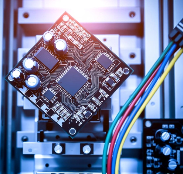
Why Does Industrial Automation Place Such Demanding Requirements on PCB Design and Assembly?
Most commercial PCBs are designed for office environments, controlled temperatures, and predictable operating conditions. Industrial automation is a completely different world — and the gap between those two worlds is exactly where reliability problems begin.
Industrial automation PCBs face four simultaneous stresses that commercial-grade designs are not built to handle: thermal cycling across extreme temperature ranges, continuous mechanical vibration from nearby machinery, chemical and moisture exposure on the factory floor, and high-intensity electromagnetic interference from power switching equipment. Each stress attacks a different part of the board, and they often compound each other.
Understanding these failure mechanisms is the starting point for making better design and sourcing decisions. Each one has a specific engineering response — and each response has direct cost and specification implications.
The Four Failure Mechanisms That Define Industrial PCB Requirements
Thermal cycling is the most consistent long-term reliability threat. As a board heats and cools through daily operation cycles, copper traces and solder joints expand and contract at different rates than the substrate beneath them. Over thousands of cycles, this differential movement initiates micro-cracks in solder joints. Those cracks propagate slowly and create intermittent failures that are extremely difficult to diagnose in the field. Every 10°C rise in steady-state operating temperature reduces component lifespan by approximately 50%. A board running 20°C hotter than the design intent will last roughly 75% less time than expected — a significant issue for equipment with a ten- or fifteen-year planned service life.
Vibration and mechanical shock attack from a different direction. Motor drives, stamping presses, conveyor systems, and robotic actuators generate continuous low-frequency mechanical energy. SMT solder joints on heavy components — transformers, large capacitors, terminal blocks — develop heel cracks under this sustained stress even when the joints look visually acceptable. Through-hole joints, where the component lead passes through the board and bonds on both sides, resist this far better.
Moisture, humidity, and chemical contamination drive electrochemical migration. Ionic residues from flux, industrial cutting fluids, and cleaning solvents create conductive pathways between conductors under voltage. The result is leakage current, trace corrosion, and eventually hard short circuits. The process is invisible until the board fails.
EMI from industrial power equipment is both immediate and cumulative. Variable frequency drives, servo amplifiers, and high-current contactors generate broadband interference across both power rails and free space. This corrupts digital signal lines, triggers false sensor readings, locks up microcontrollers, and causes unpredictable system behavior that software cannot reliably filter.
| Failure Mechanism | Primary Target on Board | Typical Failure Timeline | Engineering Response |
|---|---|---|---|
| Thermal cycling | Solder joints, plated vias | Months to years | Substrate selection, thermal vias |
| Vibration / shock | SMT joints on heavy parts | Months to years | Mixed THT/SMT assembly |
| Moisture / chemicals | Copper traces, bare pads | Weeks to months | Conformal coating |
| EMI / ESD | ICs, analog signal circuits | Immediate to months | Stackup design, I/O protection |
These stresses do not operate independently. A solder joint that survives normal thermal cycling may fail quickly under simultaneous vibration. A trace with minor conformal coating gaps corrodes faster in high humidity and chemical exposure. A robust industrial PCB design addresses all four mechanisms in parallel — not sequentially, and not on separate boards from a design and manufacturing standpoint.

Which PCB Material Is Actually Right for Your Industrial Automation Application?
Material selection is one of the earliest decisions in an industrial PCB project — and one of the most irreversible. Changing substrates after fabrication means scrapping the entire build. Getting it right requires matching the material to the actual operating environment, not to what the last project used or what costs less this quarter.
For most industrial automation applications, High-Tg FR-4 — rated to approximately 180°C — delivers the right balance of thermal performance and cost. Polyimide is specified when temperatures exceed 200°C or when thousands of rapid thermal cycles will occur over the product’s service life. Ceramic and PTFE laminates serve high-frequency RF and power modules specifically.
The practical differences between these materials are not just numbers on a datasheet. They affect fabrication process, manufacturing lead time, assembly compatibility, and long-term field behavior.
FR-4, High-Tg FR-4, and Polyimide: Where Each One Belongs
Standard FR-4 has a glass transition temperature (Tg) of approximately 100°C. Above that point, the resin matrix softens and the board loses dimensional stability. In factory environments near motors, inside poorly ventilated enclosures, or in outdoor equipment, ambient temperatures frequently approach or exceed this threshold. Standard FR-4 is not an appropriate choice for industrial automation.
High-Tg FR-4 uses a modified resin system that extends the stable operating range to approximately 180°C. More importantly, its lower coefficient of thermal expansion (CTE) reduces mechanical stress on plated through-hole vias during temperature cycling — which is the primary cause of via barrel cracking in multilayer boards. High-Tg FR-4 supports all standard PCB fabrication processes, is widely available from qualified manufacturers in Shenzhen, and is the correct baseline specification for the large majority of industrial control boards, motor drive controllers, and PLC I/O modules.
Polyimide sustains temperatures beyond 250°C and maintains mechanical integrity through thousands of rapid thermal cycles. Its moisture absorption is lower than FR-4, which benefits outdoor and high-humidity installations. The trade-off is a significantly higher per-board cost, longer fabrication lead times, and the need for careful moisture-controlled storage before lamination. Polyimide is justified for applications such as downhole drilling electronics, high-temperature oven control boards, and industrial equipment positioned directly adjacent to heat-generating machinery.
| Substrate | Max Operating Temp | Typical Industrial Application | Relative Cost |
|---|---|---|---|
| Standard FR-4 | ~100°C | Not recommended for industrial | Low |
| High-Tg FR-4 | ~180°C | PLC boards, motor drives, indoor controllers | Medium |
| Polyimide | >250°C | High-temp zones, outdoor harsh environments | High |
| Ceramic | >300°C | RF modules, precision power electronics | Very High |
One detail that is frequently overlooked at the material specification stage: copper weight. Standard 1 oz copper requires approximately 200 mils (5mm) of trace width to carry 10A without excessive temperature rise. Industrial motor drives and power conversion boards that handle 30A–50A bus currents require 3 oz or 4 oz copper pours, embedded copper bus bars, or laminated bus structures. Not all PCB fabricators support heavy-copper processing. This capability must be confirmed with the manufacturer before design finalization — not after a quote has been accepted.
Substrate selection should always originate from a documented thermal profile of the real installation environment, the planned service life in years, and the number of annual thermal cycles the board will experience. IPC-4101 provides the industry framework for matching specific material properties to application requirements.

How Do You Build EMI Control Into an Industrial PCB Before Production Starts?
EMI problems discovered during CE or FCC certification testing are expensive to fix. A board re-spin triggered by EMC failures costs three to six weeks of delay and a complete new production run. Building EMI control into the design from the start costs almost nothing extra — and produces first-pass certification results.
EMI control in industrial automation PCB design starts at the layer stackup: ground planes adjacent to every signal layer, physically partitioned analog and digital circuit areas, and impedance-controlled routing on high-speed data lines. Board-level shielding, ferrite filtering on power rails, common-mode chokes on I/O lines, and transient protection on every external interface complete the defense. These are not optional enhancements — they are structural requirements for any industrial board that operates near power switching equipment.
Layer Stackup Architecture: The Foundation of EMI Control
A 4-layer stackup — signal, ground, power, signal — is the practical minimum for any industrial board that combines power and digital data. For complex motor drive controllers or PLC CPU modules, 6-layer or 8-layer stackups provide substantially better performance:
- Every signal layer is placed adjacent to a solid ground plane, providing a clean, low-impedance return path for every routed signal
- Power planes are sandwiched between ground planes, reducing power distribution network impedance and suppressing high-frequency noise on supply rails
- Analog signal layers are placed as far as possible from digital switching layers
- Clock signals and high-speed data lines route on internal layers where radiation is lowest
Physical circuit partitioning within the board area supports the stackup. Analog sensor signal processing — 4-20mA current loop receivers, thermocouple front-ends, strain gauge amplifiers — cannot share a ground reference with digital switching circuits. A 16-bit ADC measuring a pressure transmitter signal will lose meaningful resolution if its reference ground is contaminated by a nearby switching regulator. The correct approach creates separate analog and digital regions on the board, connected at a single defined star-ground point.
Protecting Every Interface That Connects to External Wiring
Every cable that enters or leaves an industrial PCB carries noise from the external environment directly onto the board. Field wiring runs across factory floors alongside motor power cables, pick up common-mode interference, and deliver it to the PCB’s I/O pins. Standard interface protection for industrial automation PCB design includes:
- Common-mode chokes on RS-485, CAN bus, Profinet, and EtherCAT ports — these reject noise common to both signal wires without affecting the differential data signal
- TVS diodes on every external I/O line — transient voltage suppression clamps ESD and surge events before they reach IC input pins
- Optocouplers with 2500V isolation between field wiring and logic circuits — required on PLC digital input modules handling 24VDC field signals
- Ferrite beads in series with power rails entering sensitive analog sections — these provide high-frequency impedance without introducing DC resistance losses
- Shielding cans over RF sections, crystal oscillators, and precision analog front-ends where radiated interference must be contained within a defined board area
A PCB designed correctly for EMI is positioned well for EMC certification testing. Proper ground plane architecture, partitioned analog/digital areas, and protected I/O interfaces consistently produce better first-pass CE and FCC results — reducing certification time and eliminating costly post-certification design modifications.
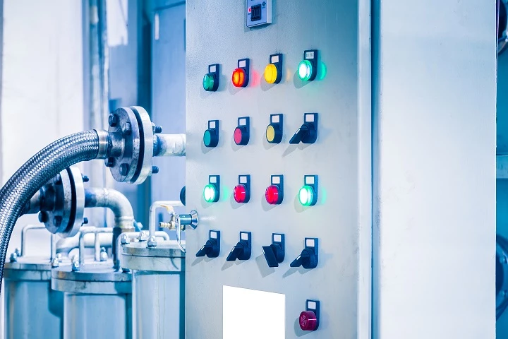
What Does Professional Industrial PCB Assembly Actually Involve?
Two manufacturers quote the same board. One is 40% higher. The price difference is invisible in the Gerber files. It becomes visible in field failure rates eighteen months after delivery.
Professional industrial PCB assembly is defined by three things: IPC J-STD-001 and IPC-A-610 Class 2 or Class 3 process certification, reflow profiles validated per specific board design, and mixed SMT/through-hole technology that places the structurally correct assembly method on each component type. Documentation and process control records — not price alone — are the accurate indicators of long-term output quality.
SMT vs. Through-Hole: The Decision That Directly Affects Field Life
Surface mount technology (SMT) is the correct assembly method for most signal-level industrial components: microcontrollers, communication ICs, discrete resistors and capacitors, and the majority of active components on a control board. SMT supports high component density and automated high-speed placement at production scale.
Through-hole assembly is non-negotiable for specific component categories. The mechanical bond created by soldering a component lead through the board on both sides is fundamentally stronger than an SMT surface bond. This difference matters directly under sustained vibration and during maintenance operations where connectors are physically disconnected and reconnected.
| Component Type | Correct Assembly Method | Primary Reason |
|---|---|---|
| MCU, FPGA, logic ICs | SMT | Density, availability, performance |
| Resistors, capacitors (signal level) | SMT | Automated placement, cost efficiency |
| Terminal blocks, field connectors | Through-hole | Mechanical extraction and insertion forces |
| High-current power connectors | Through-hole | Vibration resistance, structural bond strength |
| Electrolytic capacitors in power supply | Through-hole | Thermal cycling reliability over service life |
| Transformers, relays, large inductors | Through-hole | Mass-to-footprint ratio and vibration stress |
Mixed-technology assembly requires specific process expertise: reflow profiles must protect through-hole components that will later go through selective soldering, cleaning cycles must be compatible with both flux types, and selective solder programs must not contaminate adjacent SMT pads on the secondary side. This is a meaningful capability distinction between industrial-grade assembly operations and general-purpose contract manufacturers.
IPC Standards and What They Actually Mean for Your Boards
J-STD-001 defines the process: solder alloy specifications, flux chemistry, cleaning requirements, and reflow and wave solder process parameters. It governs how the board is assembled.
IPC-A-610 defines the result: minimum solder fillet heights, maximum BGA joint voiding percentages, acceptable through-hole fill levels, and the precise boundary between a process indicator and a rejectable defect. It governs how the output is inspected and accepted.
IPC Class 2 applies to industrial electronics where continued performance is required but limited downtime is tolerable. IPC Class 3 applies to equipment where continuous uninterrupted operation is critical — the acceptance criteria are tighter, defect tolerances are lower, and lot-level traceability documentation is required throughout the build. For industrial automation equipment that will run unattended for years, Class 3 specification is worth the marginal cost difference.
Reflow profile validation is the step that separates serious industrial PCBA manufacturers from commodity assembly houses. Every PCB design has a unique thermal mass. A dense 10-layer motor drive board absorbs heat differently than a simple 2-layer I/O module. A single standard profile applied to all board types simultaneously produces cold joints on thermally heavy sections and thermal damage near the board edge. Professional operations validate profiles using thermocouple-instrumented test boards before production begins, and maintain profile records per order for process traceability.
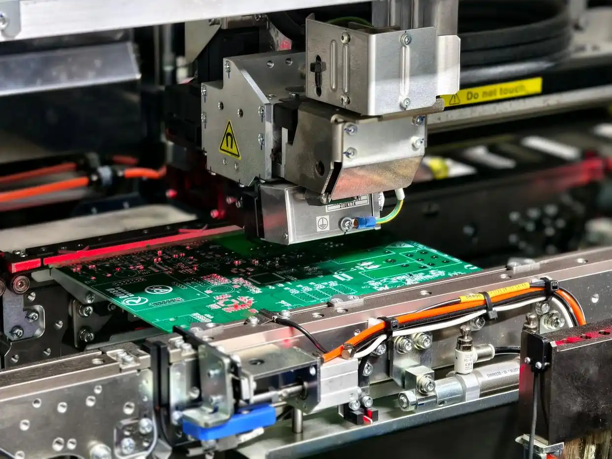
How Do You Choose the Right Conformal Coating for Your Industrial Environment?
Conformal coating is the final environmental barrier between a finished PCB assembly and the conditions it will actually face in service. The wrong coating chemistry for the deployment environment — or no coating at all — is one of the most predictable and preventable causes of industrial field failures.
Conformal coating selection is determined by the actual operating environment. Silicone coatings handle extreme thermal cycling ranges and outdoor use. Urethane coatings resist industrial chemicals and mechanical abrasion. Acrylic coatings serve moderate-humidity indoor environments where rework access may be needed. Epoxy coatings provide maximum moisture and chemical protection where board repair is not anticipated. No single coating is optimal across all industrial conditions.
Matching Coating Chemistry to Deployment Environment
| Coating Type | Best Deployment Environment | Temperature Range | Reworkable? |
|---|---|---|---|
| Acrylic (AR) | Moderate humidity, indoor factory | -65°C to 125°C | Yes |
| Urethane (UR) | Solvent exposure, chemical-rich environments | -65°C to 125°C | Difficult |
| Silicone (SR) | Extreme temperature swings, outdoor, high humidity | -65°C to 200°C | Very difficult |
| Epoxy (ER) | Aggressive chemical exposure, immersion risk | -65°C to 150°C | No |
One practical decision factor that is often missed at specification time: if the board will ever need component-level repair in the field, the coating determines whether that repair is feasible. Acrylic coatings dissolve with standard solvents and allow clean rework. Silicone and epoxy coatings require mechanical removal and frequently damage the board surface. For boards expected to run maintenance-free through their full service life, this tradeoff is acceptable. For boards installed in locations where field repairs are standard practice, it is not.
Application Method and Coverage Verification
Spray application is fast but produces inconsistent film thickness over tall components and in the gaps between densely packed parts. Selective robotic dispensing applies coating to precisely defined board areas with consistent film thickness regardless of board topology. For production volumes above a few hundred units, selective robotic dispensing is the professional standard method.
Coverage verification is performed under UV illumination after coating cures. Most industrial conformal coatings contain UV-fluorescent additives that make coverage gaps immediately visible. This inspection step is required under IPC-A-610 and IPC-CC-830C. Boards with coverage voids return for re-coating. Areas that must remain uncoated — connector contacts, test points, heat sink mounting surfaces — are protected by selective dispensing program boundaries, eliminating the masking and de-masking labor required with spray processes.
How Do You Validate an Industrial PCBA Before It Reaches the Field?
Visual inspection alone does not catch the defects that cause industrial field failures. A board that looks correct can have BGA joints with 40% voiding, through-hole barrel fill below the Class 3 minimum, or a cold solder joint on a power connector that will open under its first thermal cycle. Staged test protocols exist to catch these — before deployment, not after.
Professional industrial PCBA validation uses five sequential inspection and test stages. Each stage catches a different defect category. Skipping stages shifts defect detection from the factory to the field — where detection is ten to a hundred times more expensive.
The Five-Stage Industrial PCBA Test Protocol
Stage 1 — Automated Optical Inspection (AOI): After solder paste printing and after reflow, AOI systems scan 100% of boards. They catch missing components, polarity reversals, solder bridges, lifted leads, and tombstoned passives. AOI at both stages — pre and post-reflow — identifies process drift before it affects more than a single panel.
Stage 2 — X-ray Inspection (AXI): For multilayer boards and assemblies with BGA, QFN, LGA, or press-fit connectors, X-ray inspection verifies joint voiding, internal bridging, and seating depth for features that are physically hidden from optical inspection. 3D AXI provides cross-sectional void percentage measurement for BGA joints — essential for motor drive boards where power BGA devices are used in high-thermal-stress positions.
Stage 3 — In-Circuit Test (ICT): A bed-of-nails ICT fixture applies electrical probes to predefined test points and verifies component presence, correct value, polarity, and basic circuit connectivity. Well-implemented ICT achieves approximately 85–95% defect coverage. ICT is the production-gate that prevents defective boards from entering functional test queues and inflating test station time.
Stage 4 — Functional Test (FCT): The assembled board powers up and runs through its full operational sequence under simulated application conditions. For an industrial motor drive controller, this means verifying PWM output accuracy, current measurement calibration across the full ADC range, fault detection logic response times, and communication protocol handshake behavior. Functional test confirms the board works — not just that it is assembled correctly.
Stage 5 — Burn-In Testing: For Class 3 and high-reliability applications, assembled boards run at elevated temperature — typically 85°C ambient — and full operating voltage for 24 to 168 hours while cycling through operational patterns. This accelerated stress period screens for infant mortality failures: component weaknesses and marginal solder joints that would cause early field failure but cannot be detected by electrical test at room temperature. Industry data consistently shows that 70% of electronic field failures occur within the first operational months if infant mortality screening is not performed. Burn-in programs reduce field failure rates in critical applications to below 0.1%.
What Should Overseas Clients Actually Look for in a China-Based Industrial PCB Partner?
The price difference between a qualified industrial PCB manufacturer and a general-purpose commodity shop is typically 15–25% per board. The total cost difference — when field failures, replacement logistics, production downtime, and engineering investigation time are included — frequently exceeds the original board value by a factor of five to ten. Evaluating a China-based industrial PCB partner on price per board is the wrong metric.
A qualified industrial PCB design, reverse engineering, and manufacturing partner should be evaluated on four dimensions: documented process certifications, demonstrated technical capability in industrial-specific processes, complete service scope from design through production, and communication quality across languages and time zones.
Certifications That Confirm Real Process Capability
| Certification | What It Confirms |
|---|---|
| ISO 9001:2015 | Documented quality management system, audited processes, corrective action procedures |
| IPC Class 2 / Class 3 capability | Workmanship standards for industrial or high-reliability electronics assembly |
| UL 94 V-0 material qualification | All substrate materials meet required flammability standards |
| RoHS compliance processes | Assembly processes and component sourcing meet EU RoHS and equivalent regulations |
| IPC J-STD-001 certification | Soldering process meets defined standards for industrial electronics |
IEC 61508 familiarity — the functional safety standard for industrial equipment — is an additional qualification marker for clients producing safety-rated automation systems.
The One-Stop Advantage: Why It Reduces Project Risk
Fragmenting PCB design, fabrication, component sourcing, and assembly across multiple vendors introduces handoff risks: Gerber interpretation errors, component substitutions that change electrical performance, and assembly processes not optimized for the specific substrate. Every vendor boundary is a potential failure point.
IWDF Solutions provides the complete industrial PCB service stack from a single accountable team in Shenzhen: industrial PCB design from concept schematic through production-ready Gerbers with DFM review, PCB reverse engineering and cloning from physical samples, PCB fabrication up to 32 layers including heavy copper and high-Tg options, full PCBA production under IPC J-STD-001 and IPC-A-610 Class 2/3, complete AOI/AXI/ICT/FCT/burn-in testing, and conformal coating application with UV verification.
For overseas clients, English-language engineering communication, responsive technical quoting, and standard file format delivery — Gerber RS-274X, ODB++, IPC-2581 — are practical differentiators that reduce the risk of specification errors in production. IWDF Solutions maintains strict NDA and intellectual property protection procedures for all client design files, with documented access controls and data handling policies.
Frequently Asked Questions
Q: What is the difference between IPC Class 2 and Class 3 for industrial PCB assembly?
IPC Class 2 covers industrial and commercial electronics where continued performance is required and limited repair downtime is acceptable. IPC Class 3 covers high-reliability applications where uninterrupted operation is critical. Class 3 sets tighter solder joint acceptance criteria, lower defect tolerances, and requires complete lot-level traceability records. For industrial automation equipment running unattended for years, Class 3 is the appropriate specification.
Q: When should through-hole assembly be used instead of SMT for industrial automation PCBs?
Through-hole assembly is required for connectors subject to physical mating and unmating forces, high-current power connectors above 20A, heavy passive components including large electrolytic capacitors and power transformers, and any component that must resist sustained mechanical vibration. Most industrial boards use mixed-technology assembly — SMT for signal-level components, through-hole for mechanically stressed parts.
Q: How do I know which conformal coating is right for my industrial environment?
Start with the operating temperature range and chemical exposure profile. Acrylic coatings are correct for moderate-humidity indoor environments where rework may be needed. Urethane suits environments with solvent or chemical exposure. Silicone handles extreme thermal cycling and outdoor applications. Epoxy provides maximum protection in aggressive chemical or immersion-risk environments where repairability is not required.
Q: What information does IWDF Solutions need to begin a PCB reverse engineering project?
The physical PCB sample is the primary input. For multilayer boards, X-ray imaging is used to capture internal layers non-destructively. A description of the original equipment, approximate board age, and any available functional documentation — even partial — helps accelerate the component identification and schematic verification steps. IWDF Solutions handles the full process from physical sample to production-ready Gerber package.
Q: What causes early field failures in industrial PCBs even when initial testing passes?
Early field failures most commonly result from marginal solder joints that pass room-temperature electrical testing but fail under thermal cycling stress in the field, incorrect conformal coating specification for the actual operating environment, inadequate EMI design in boards installed near variable frequency drives or high-current switching equipment, and substrate material choices that are not rated for the actual thermal profile of the installation location. These are design and specification decisions, not random manufacturing events — and they are preventable with the right engineering process before production begins.
Q: How long does a typical PCB design and assembly project take at IWDF Solutions?
Standard industrial PCB design projects from schematic to production-ready Gerbers typically require 2–4 weeks depending on board complexity. PCB fabrication of multilayer industrial boards is 7–15 working days. SMT and through-hole PCBA production, including AOI and functional test, is 5–10 working days after fabrication. For projects requiring full PCB reverse engineering before fabrication, the reverse engineering phase adds 5–15 days depending on layer count and component complexity. Expedited timelines are available for urgent projects.
Industrial automation PCBs operate in conditions that reveal every design shortcut and every process compromise. The manufacturing partner you select determines not just what you pay per board, but what your equipment costs to operate over a ten- or fifteen-year service life. IWDF Solutions provides PCB design, reverse engineering, fabrication, and full PCBA production for industrial automation clients across Europe, North America, Southeast Asia, and the Middle East from a single team in Shenzhen.
Contact IWDF Solutions to discuss your industrial project PCB design or assembly requirements and receive a project-specific technical consultation.

