

EV powertrains fail at the board level more often than engineers admit. Wrong copper weight, bad material choices, and missing isolation distances destroy programs that had every other variable right.
High-reliability PCB design and assembly for EV power electronics means matching materials, stackup, copper weight, isolation geometry, and assembly process controls to the specific operating conditions of each subsystem — traction inverter, OBC, DC-DC converter, or BMS. One generic PCB specification applied across all four subsystems is not a design decision. It is a liability.
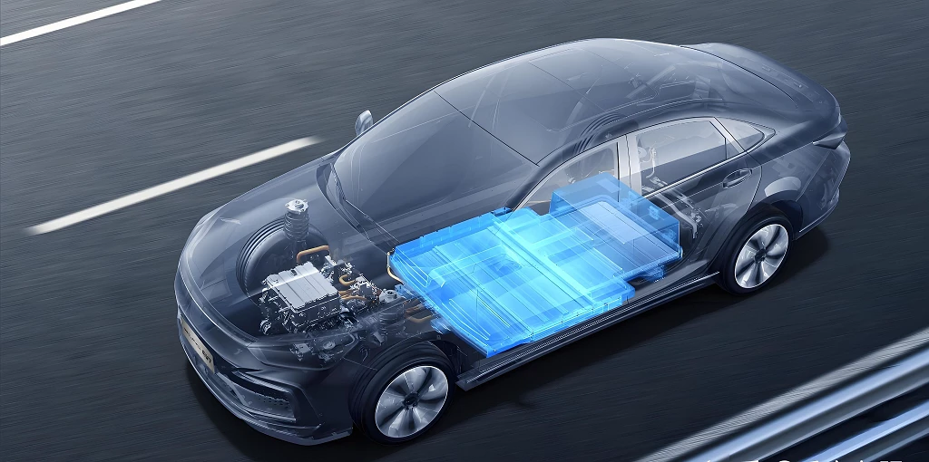
The global automotive PCB market is on track to reach USD 11.91 billion by 2030, driven almost entirely by EV adoption. An electric vehicle carries roughly 50% more PCBs than an internal-combustion vehicle — and each of those boards operates inside an electrical environment that would destroy a standard consumer-grade PCB within weeks: 400–800V bus voltages, hundreds of amps, thousands of thermal cycles, and a 10–15 year service life requirement. Every section below addresses a specific design or sourcing decision that determines whether an EV power board survives the field or fails during qualification.
What Makes an EV Power Electronics PCB “High-Reliability” in the First Place?
A high-reliability EV power electronics PCB is not defined by a single standard. It is defined by the combination of material Tg, copper weight, clearance and creepage distances, assembly process class, and post-assembly test coverage that matches the electrical and thermal stress each subsystem will see across a 10–15 year service life.
The four main subsystems in an EV powertrain each place specific demands on their PCB. A specification that works for the BMS sensing board is structurally inadequate for the traction inverter gate driver — and vice versa.
EV Powertrain Subsystems and Their PCB Requirements
| Subsystem | Bus Voltage | Peak Current | Primary PCB Design Challenge |
|---|---|---|---|
| Traction Inverter | 400–800V DC | 300–600A | Gate loop inductance, dV/dt stress, EMI |
| On-Board Charger (OBC) | 220V AC → 400–800V DC | 20–50A | Galvanic isolation barrier, PFC harmonics |
| DC-DC Converter | 400–800V → 12–48V | 50–200A | Thermal dissipation, galvanic isolation |
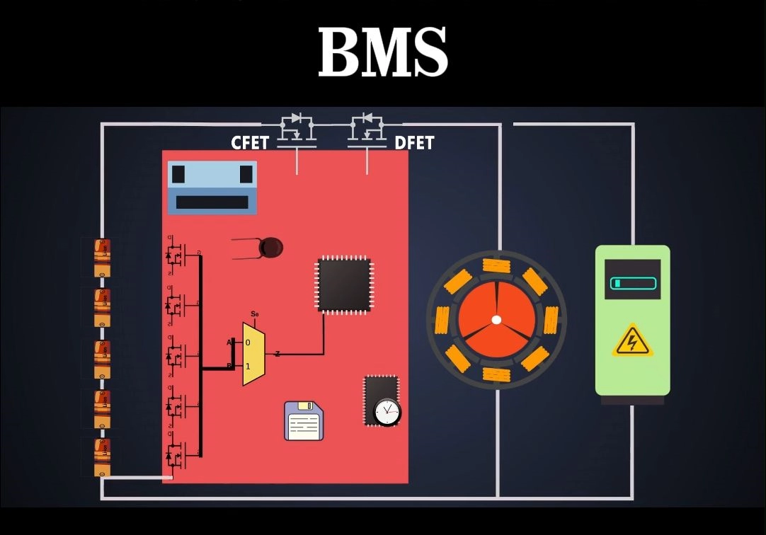
| Battery Management System (BMS) | 3.2–4.2V per cell / up to 800V total | 1–5A sensing path | Millivolt-level accuracy, common-mode rejection |
The BMS PCB, for example, must measure individual cell voltages to within ±3–5mV while sitting in the presence of 800V common-mode voltages and 500A pack currents. The traction inverter gate driver PCB must hold gate loop inductance below 10nH while routing an 800V-rated isolation barrier on the same board. These are not goals — they are functional requirements. Any board that does not meet them will either fail qualification testing or degrade silently until a field failure occurs.
Standard FR-4 laminates have a glass transition temperature of 130–140°C — below the junction temperatures SiC power modules generate under normal operating load. A 1oz copper trace wide enough to pass default DRC checks will still overheat carrying traction inverter currents. And the clearance distances baked into most PCB CAD default rule sets were written for 48V or 230V designs, not 800V automotive power electronics.
Understanding why standard practices fall short is the foundation of every high-reliability EV PCB program. The next question is which materials actually survive the conditions described above.
Which PCB Materials Actually Ensure High-Reliability Performance Inside an EV Power Module?
Specifying “FR-4” on an EV power board drawing is like specifying “steel” for a structural part. The category is too broad. The wrong choice within that category causes board-level failures that are expensive to trace back to material selection.
Material selection for high-reliability EV power boards requires matching glass transition temperature (Tg), comparative tracking index (CTI), and thermal conductivity to the specific heat load and voltage stress of each subsystem. The traction inverter power stage and the BMS control board require fundamentally different materials — and a supplier who quotes the same laminate for both has not read your thermal analysis.
Matching Material to Subsystem
High-Tg FR-4 (Tg ≥ 170°C), halogen-free: Appropriate for BMS analog front-end boards and OBC control sections where temperatures stay below 150°C. The higher Tg prevents delamination across the 2,000+ thermal cycles that automotive qualification requires. Halogen-free grades add flame resistance ratings that meet UL 94 V-0 without brominated additives.
High-CTI, high-Tg laminates (CTI ≥ 600V, Group I per IEC 60112): Required for all boards where high-voltage traces and low-voltage signals coexist on the same layer. A CTI ≥ 600V material allows shorter creepage distances at 800V working voltage. A low-CTI material at the same voltage requires substantially wider spacing — sometimes making the design physically impossible at the required board size.
Rogers RO4350B and equivalent hydrocarbon/ceramic laminates: Used for gate driver boards supporting SiC or GaN devices. Standard FR-4 has an unstable dielectric constant across temperature. RO4350B maintains a consistent Dk of 3.48 ± 0.05 from -40°C to +150°C. Stable Dk matters for controlled impedance routing of isolated SPI and gate signal traces — predictable impedance means predictable switching behavior.
Insulated Metal Substrates (IMS) and Metal Core PCBs (MCPCB): Required for power-stage components where heat dissipation is concentrated — SiC MOSFET drive stages, snubber networks, high-current shunts. IMS boards with aluminum base and ceramic-filled dielectric achieve 2–8 W/mK thermal conductivity. Direct bonded copper (DBC) on ceramic reaches 400 W/mK. These materials reduce thermal resistance by 5–10× compared to standard FR-4, enabling stable operation at SiC junction temperatures approaching 250°C.
Material Selection by Subsystem
| Subsystem | Recommended Material | Min. Tg | Key Reason |
|---|---|---|---|
| BMS sensing and control | High-Tg halogen-free FR-4 | 170°C | Thermal cycling stability |
| OBC gate driver and control | High-CTI halogen-free laminate | 170°C | Isolation at 400–800V |
| Traction inverter power stage | IMS or DBC ceramic | N/A | Power density, high Tj |
| DC-DC converter | Rogers RO4350B or high-Tg FR-4 | 170°C | Stable Dk at high switching frequency |
Getting material right sets the boundary conditions for everything else. Once material is confirmed, the next design variable — copper weight — determines whether the board can actually carry the currents the system demands.
How Does Copper Weight Define High-Reliability EV PCB Design for High-Current Applications?
A trace that passes every design rule check at 1oz copper will still overheat carrying 100A of inverter bus current. DRC compliance and thermal compliance are not the same thing.
High-reliability EV power boards require 2oz to 6oz copper for power planes and high-current traces. Traction inverter and DC-DC converter boards sometimes reach 10–14oz for traces that replace busbars. The correct copper weight depends on current density, allowable temperature rise, layer count, and heatsink coupling — not on what the factory quotes as a standard offering.
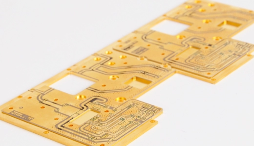
Copper Weight vs. Current Capacity
IPC-2152 defines current capacity as a function of copper weight, trace width, and allowable temperature rise. For EV power applications, the design target is a maximum 10°C rise above ambient — not the 30°C that is commonly accepted for consumer boards.
| Copper Weight | Thickness | Approx. Max Continuous Current (10°C rise, 5mm wide trace) | Typical EV Application |
|---|---|---|---|
| 1oz | 35μm | ~8A | BMS signal routing, CAN bus traces, gate drive signal layers, isolated SPI lines |
| 2oz | 70μm | ~14A | BMS power supply planes, OBC control board power rails, low-side gate driver supply traces |
| 3oz | 105μm | ~20A | DC-DC converter power planes, OBC secondary-side current paths, cell balancing discharge traces |
| 6oz | 210μm | ~35A | Traction inverter gate driver power stage, high-current BMS protection switching paths |
| 10oz | 350μm | ~55A | Busbar-replacement traces in traction inverter boards, main pack current distribution in high-power DC-DC converters |
| 14oz | 490μm | ~70A+ | Direct busbar replacement for 200A+ continuous current paths, EV charging inlet distribution boards |
These values assume still air with no forced cooling. With an aluminum heat sink and a thermal via array, a 6oz copper pour at 20mm wide can carry well over 200A continuously — the table reflects conservative baseline figures, not design maximums.
In practice, most EV power boards use mixed copper weights across layers: 1oz on signal layers, 2–3oz on inner power planes, and heavy copper (6oz+) only on the outer layers where high-current traces and thermal pads are located. This mixed-weight approach reduces fabrication cost while concentrating copper where the heat load actually is.
Heavy Copper Fabrication: What Buyers Must Specify
Heavy copper boards (≥3oz) require wider etch tolerances — typically ±15% of nominal trace width — because chemical etching becomes less controlled at greater copper depth. Designers must calculate minimum conductor cross-section at worst-case minimum copper thickness, not nominal. Factories that skip this step during DFM review produce boards with undersized power traces that fail current capacity tests after assembly.
Thermal vias beneath high-dissipation components must be treated as a system:
- Grid spacing: ≤0.8mm center-to-center
- Drill diameter: 0.2–0.3mm
- Plating: ≥25μm copper per IPC-6012 Class 3
- Cap or fill vias where component pads require a flat soldering surface
A 5×5 thermal via array under a TO-247 SiC MOSFET reduces junction-to-heatsink thermal resistance by approximately 30% compared to the same board without vias. That directly reduces operating temperature and extends device service life.
With copper weight and materials defined, the next decision — layer stackup — determines whether the board can physically separate high-voltage from low-voltage domains and still route all required signals.
What Layer Stackup Does a High-Reliability EV Power Electronics PCB Actually Require?
Choosing the wrong layer count does not just add board cost. It can make EMC compliance physically impossible and prevent the isolation distances that 800V operation requires.
High-reliability EV power boards use 4-layer stackups for BMS control, 6-layer for OBC and gate driver boards, and 8 or more layers for traction inverter and integrated power stages. The stackup must place solid ground planes adjacent to all signal layers and must physically separate high-voltage from low-voltage copper on every layer — not just the outer layers.
Stackup Configurations by Subsystem
4-Layer (BMS Control): TOP (signals) → GND (solid plane) → PWR → BOTTOM (signals). The solid ground plane immediately beneath the top signal layer provides a low-impedance return path and suppresses common-mode noise coupling from adjacent high-current cell connections. Supports 120Ω controlled impedance for CAN bus differential pairs.
6-Layer (Gate Driver and OBC Control): TOP → GND → SIG → SIG → GND → BOTTOM. Dedicated inner signal layers are sandwiched between ground planes. This structure supports isolated SPI routing at 50Ω and handles voltage domain separation between gate driver primary and secondary sides on a single board.
8-Layer (Traction Inverter Power Stage): TOP → GND → SIG → PWR → PWR → SIG → GND → BOTTOM. Symmetrical ground plane placement at layers 2 and 7 provides the broadside capacitance that suppresses common-mode noise across the entire board. High-voltage traces are confined to outer layers. No copper from any inner layer — including ground pour — crosses the HV keepout boundary.
Controlled Impedance by Signal Type
| Signal Type | Target Impedance | Tolerance |
|---|---|---|
| CAN bus differential pair | 120Ω differential | ±10% |
| Isolated SPI (gate driver) | 50Ω single-ended | ±10% |
| Gate drive trace | Minimize total length — not impedance controlled | Loop L < 10nH |
| Power plane | Minimize ESR and ESL | Verified by simulation |
Impedance-controlled boards require a locked and documented stackup from the fabrication stage. Any dielectric material substitution by the PCB factory — without a formal engineering change notification — changes the impedance profile and invalidates the controlled impedance specification. This must be written as a purchase order requirement before fabrication starts.
The stackup defines where high-voltage copper can physically exist. The next step is setting the exact clearance and creepage numbers that prevent 800V arcing failures between those copper layers and everything adjacent to them.
How Do Creepage and Clearance Rules Define High-Reliability PCB Design at 400–800V?
A board can pass every geometric DRC check and still fail hi-pot testing. The reason is almost always creepage and clearance values that were set for the wrong voltage range or the wrong standard.
At 800V working voltage in a Pollution Degree 2 automotive environment, minimum clearance through air exceeds 8mm and minimum creepage along an uncoated PCB surface reaches 12.5mm or more depending on base material CTI. Standard PCB CAD default rule sets are built for 48V or 230V — not 800V automotive power electronics. These rules must be replaced before layout begins, not corrected during design review.
Clearance vs. Creepage: The Practical Difference
Clearance is the shortest distance through air between two conductive parts. It depends on working voltage, overvoltage category, and altitude.
Creepage is the shortest path along the surface of insulating material between two conductive parts. It depends on voltage, pollution degree, and the CTI rating of the base material.
Both are defined in IEC 60950, IEC 62368, and IPC-2221. EV inverter power stages follow IEC 62477. Safety-critical vehicle circuits also carry ISO 26262 requirements on top of those IEC standards. The governing standard for each subsystem must be confirmed before design rules are set.
Minimum Required Distances at EV Operating Voltages
| Working Voltage | Min. Clearance (Cat. III) | Min. Creepage (CTI Group II, PD2, uncoated) |
|---|---|---|
| 300V | 3.0mm | 4.0mm |
| 600V | 5.5mm | 8.0mm |
| 800V | 8.0mm | 12.5mm |
| 1000V | 10.0mm | 16.0mm |
Conformal coating — applied to IPC-CC-830 standard and documented per IATF 16949 traceability requirements — reclassifies the board surface from Pollution Degree 2 to Pollution Degree 1. This reduces required creepage by approximately 30–40%. That is a real engineering benefit. But it only applies when coating thickness, coverage area, and cure cycle are validated and logged for every production board. A conformal coating step that is applied informally as a last finishing operation does not qualify for this reduction.
In EV power board layouts, high-voltage keepout zones must be enforced on every layer — top, bottom, and all inner layers including ground pour fills. Physical board cutouts or slots are required at OBC primary-to-secondary isolation boundaries to meet reinforced insulation requirements. These rules must be set as locked DRC constraints in Altium, Cadence Allegro, or equivalent tools before any layout work begins.
Getting creepage and clearance right on a standard IGBT-based design is already demanding. Switching to SiC or GaN devices makes the entire layout problem harder — because those devices switch faster, and every added nanosecond of switching speed makes parasitic layout geometry matter more.
Why Do SiC and GaN Devices Raise the Bar for High-Reliability EV PCB Design and Assembly?
Replace an IGBT with a SiC MOSFET and leave the PCB layout unchanged. The device will not survive the first switching event at full load. Wide-bandgap semiconductors switch faster than the original layout was built to handle.
SiC MOSFETs switch at dV/dt rates above 50V/ns and generate voltage overshoots directly proportional to gate loop and power loop parasitic inductance. A PCB layout with 20nH of stray power loop inductance, switching 400A at 2,000A/μs, generates 40V of overshoot on top of a 400V DC bus. GaN devices extend switching frequencies to 1–10MHz, where standard via geometry and trace routing add enough parasitic inductance to cause device destruction within hours of first power-on.
Gate Driver PCB Requirements for SiC
| Design Parameter | Target Value | Consequence If Missed |
|---|---|---|
| Total gate trace length | ≤20mm | Gate ringing and oscillation |
| Gate loop inductance | <10nH | Voltage overshoot, elevated EMI |
| Kelvin source connection | Mandatory | Ground bounce corrupts gate voltage |
| Decoupling cap ESL (at driver VCC pin) | <1nH — C0G/NP0 only | Insufficient HF supply decoupling |
| Isolation barrier CMTI rating | >100kV/μs | False gate triggering during switching |
Kelvin source connection is not a best practice recommendation for SiC designs — it is a functional requirement. Without a separate Kelvin source trace, di/dt in the main power loop induces a voltage in the gate return path that modifies the effective gate-source voltage during switching transitions. The result is unpredictable turn-on and turn-off timing that correlates with load current and is extremely difficult to diagnose without detailed layout analysis.
GaN-Specific Layout Rules
GaN devices operate at 1–10MHz. At these frequencies, a single 1mm via in the gate signal path adds 0.5–1nH of inductance — significant when the total gate loop budget is under 5nH. Gate driver placement within 5mm of the GaN device is required. Enhancement-mode GaN also needs a negative turn-off voltage (typically -3V to -5V) to prevent spurious turn-on from common-mode transients. The negative rail bypass capacitor must be placed on the device side of the isolation barrier — not on the controller side where it does not affect the switching transient.
SiC and GaN devices also raise EMI emission profiles significantly compared to IGBT designs. Conducted emissions must stay within CISPR 25 Class 5 limits to protect CAN, LIN, and automotive Ethernet networks. EMI compliance at these switching speeds depends on PCB layout geometry — not just on the output filter design. Ground plane integrity, power loop geometry, and return current path continuity are all active EMI mitigation tools, not passive background features.
Once the design is complete, the quality of the assembled board depends entirely on whether the assembly process can match what the design requires. That process control question is where many otherwise well-designed EV programs lose their reliability margin.
What Assembly Process Controls Are Non-Negotiable for High-Reliability EV PCB and PCBA Production?
A correctly designed EV power board still fails field qualification if the assembly process is not controlled to the same standard. Design quality and assembly quality are not separate categories. They are one continuous risk chain.
High-reliability EV power electronics PCBA must meet IPC-A-610 Class 3, pass hi-pot dielectric withstand testing at 2,500–3,000V between all isolated domains, and include documented process traceability per IATF 16949. AOI, 3D X-ray, conformal coating with validated process parameters, and functional test are contractual requirements for automotive supply chains — not optional service upgrades.
Assembly Quality Standards for EV Power Boards
| Standard | Scope | Required Level for EV |
|---|---|---|
| IPC-J-STD-001 | Soldering requirements | Class 3 |
| IPC-A-610 | Assembly workmanship | Class 3 |
| IPC-6012 | Rigid PCB performance qualification | Class 3 |
| IATF 16949 | Automotive quality management | Supplier certification required |
| ISO 26262 | Functional safety | ASIL-B to ASIL-D by subsystem |
| AEC-Q200 / AEC-Q100 | Passive and active component qualification | Required for all EV components |
| UL 94 V-0 | Flame retardancy | Required for base material |
Reflow Profiling for Heavy Copper Boards
Heavy copper boards have significantly higher thermal mass than standard 1oz boards. A reflow profile optimized for standard PCBs will produce cold solder joints on the same design built in 6oz copper.
The preheat ramp rate above 150°C must be reduced to ≤1.5°C/s. Time above liquidus must increase to allow complete solder wetting of large thermal pads. Each unique board design in the EV product family needs its own validated thermal profile — not a shared line profile applied across all products.
Mixed-technology boards combining SMD power devices and through-hole high-voltage connectors require selective soldering after reflow. Sending mixed-tech boards through a standard wave solder process exposes assembled SMD components to thermal shock they are not rated to survive.
Inspection and Test — Minimum Requirements
- SPI (Solder Paste Inspection): Before reflow. Verifies paste volume and positional accuracy. Critical for fine-pitch BMS analog front-end ICs with sub-0.5mm pitch pads.
- AOI (Automated Optical Inspection): After reflow. Detects missing components, solder bridges, wrong polarity, and lifted leads on all boards.
- 3D X-Ray: Required for BGA, QFN, and stacked-die packages common in automotive-grade BMS AFE ICs. Solder joint quality beneath the package is invisible to AOI.
- Hi-Pot Test: Applied to every assembled board — not sampled. For 800V systems: 2,500V AC or 3,000V DC between all isolated domains, 60 seconds minimum. Any leakage current above specification is a reject — not a candidate for rework.
- Functional Test: Every board must pass a documented functional test. For BMS boards this includes cell voltage measurement accuracy verification, protection circuit trip-point confirmation, and communication interface validation. For gate driver boards it includes switching waveform quality checks at representative operating current.
Even with every one of these process controls in place, the reliability of the final product depends equally on choosing the right manufacturing partner. That decision carries its own set of risks — and its own criteria that matter more than a supplier’s marketing materials.
How Do You Identify a Genuine High-Reliability EV PCB Design and Assembly Partner in China?
Every Shenzhen PCB supplier claims automotive-grade capability. Fewer than 20% can prove it when a qualification audit arrives. The gap between the claim and the documented evidence is where programs get delayed by six months.
The right China-based partner for high-reliability EV power electronics PCB design and assembly must hold IATF 16949 certification with an automotive scope that explicitly covers PCB fabrication and assembly. They must demonstrate IPC-A-610 Class 3 process qualification with certified inspector records, provide full material and process traceability from bare board through final test report, and show direct experience with heavy copper, high-voltage isolation design, and AEC-Q100/Q200 qualified component sourcing from authorized distributors.
What to Verify Before Placing a Production Order
| Verification Item | What to Ask For | Red Flag |
|---|---|---|
| IATF 16949 certificate | Certificate with scope statement listing PCB fabrication/assembly | Certificate with “office” or “design only” scope |
| IPC-A-610 Class 3 | Certified IPC inspector credentials on staff | “We follow Class 3 internally” without certification |
| Heavy copper capability | Sample boards at ≥3oz with impedance test reports | No sample data available |
| Hi-pot test coverage | 100% hi-pot test record for EV boards shipped | Sampling-based hi-pot only |
| Component sourcing | Authorized distributor invoices for AEC-Q200 parts | “We source from the open market” |
| NDA and IP protection | Signed NDA before files are shared | Reluctance to sign before file review |
China accounts for more than 60% of global PCB production, and the Shenzhen ecosystem offers genuine structural advantages: 30–50% lower fabrication cost versus equivalent North American or European suppliers, access to the world’s deepest electronic component supply chain, and a concentration of engineering talent in EV and automotive electronics that is not replicated elsewhere. These advantages are real — but they only apply to suppliers who have built the quality management infrastructure to support automotive programs. A supplier who offers lower prices by skipping IATF 16949 audit costs is not offering value. They are transferring your program risk onto your company’s warranty liability.
One-stop service — covering PCB design, reverse engineering, bare board fabrication, PCBA, functional test, and conformal coating under one roof — eliminates the handoff failures between design and manufacturing that are the most common source of NPI delays. For EV power electronics programs where time-to-qualification is a competitive constraint, that integration is a material business advantage, not just a convenience.
IWDF Solutions: High-Reliability PCB Design and Assembly for EV Power Electronics
At IWDF Solutions, based in Shenzhen, China, PCB design and assembly for EV power electronics and BMS applications covers the full program lifecycle under one roof:
- EV PCB Design: Schematic capture through multilayer layout for BMS, traction inverter gate driver, OBC, and DC-DC converter boards — including DFM analysis, controlled impedance stack-up definition, and Design for Test planning.
- PCB Reverse Engineering: Full layer-by-layer copper extraction, BOM reconstruction, and Gerber file generation from physical boards. Supports legacy platform maintenance, obsolete board replacement, and upgrade programs that move from IGBT to SiC technology without a full system redesign.
- PCB Fabrication: High-Tg halogen-free, high-CTI, heavy copper, MCPCB, HDI, and rigid-flex construction to IATF 16949 and IPC-6012 Class 3 standards.
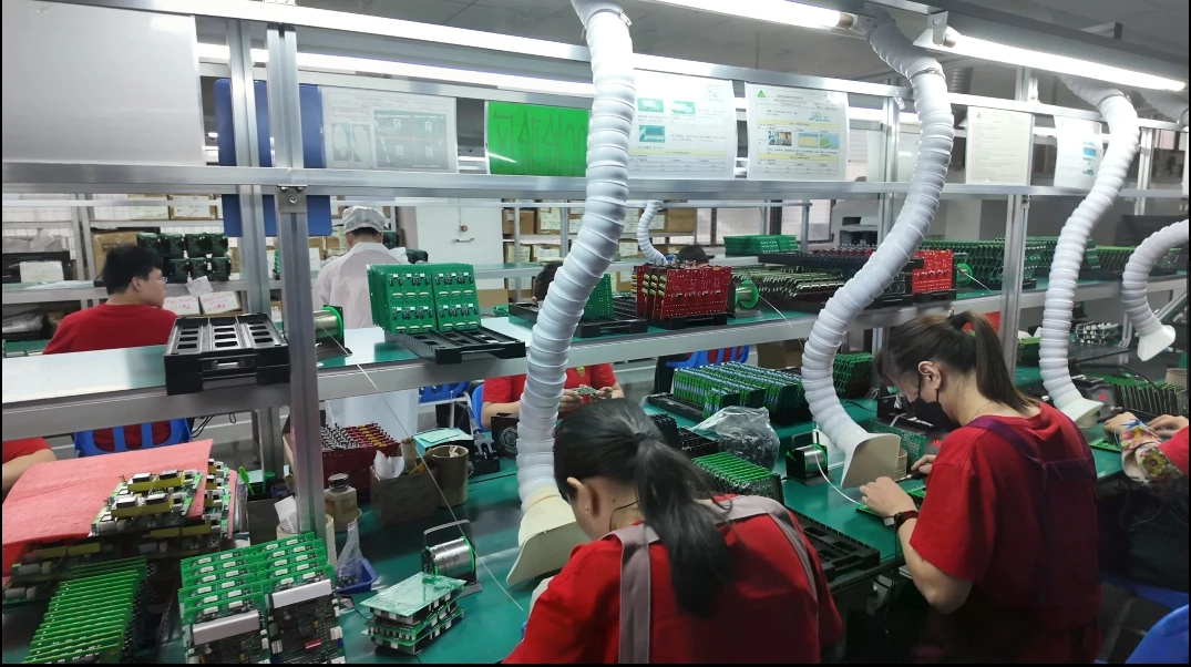
- PCB Assembly (PCBA): Automotive-grade SMT and THT assembly with SPI, AOI, 3D X-ray, 100% hi-pot testing, conformal coating, and functional test — with full process traceability per IATF 16949.
- Component Sourcing: AEC-Q200 and AEC-Q100 qualified parts from authorized distributors, with traceability documentation available for every component lot.
For B2B clients globally — whether a first prototype of a new BMS design or volume production of a qualified traction inverter gate driver board — IWDF Solutions provides the technical depth, process certification, and Shenzhen supply chain integration to support programs from NPI through sustained production volume.
Contact IWDF Solutions to discuss your EV power electronics PCB design and assembly requirements. Our engineering team will review your specifications and provide a detailed technical proposal.
Frequently Asked Questions
Q1: What is the difference between a standard automotive PCB and a high-reliability EV power electronics PCB?
A standard automotive PCB typically operates below 60V in body electronics and infotainment systems. A high-reliability EV power electronics PCB operates at 400–800V, carries hundreds of amps, and must survive 10–15 years of thermal cycling in close proximity to high-frequency switching devices. The material, copper weight, clearance distances, and assembly standards are fundamentally different categories.
Q2: How many layers does a BMS PCB typically require?
Most automotive BMS designs use 4-layer boards for sensing and control circuits. Larger, high-channel-count BMS designs with integrated cell balancing and isolated communication interfaces may require 6 layers to separate power, signal, and isolation domains cleanly. Layer count is determined by component density, isolation requirements, and controlled impedance needs — not by a fixed industry rule.
Q3: What copper weight should I specify for a traction inverter gate driver board?
Gate driver signal routing typically stays at 1oz. Power supply and gate drive current paths require at least 2oz. If the board also integrates a portion of the DC bus or high-current snubber network, 3–6oz copper on dedicated power layers is appropriate. Specify the current load and allowable temperature rise to your PCB manufacturer — copper weight follows from that thermal calculation, not from a standard template.
Q4: What conformal coating is best for EV power electronics boards?
Silicone conformal coating offers the widest temperature range (-65°C to +200°C) and best performance under vibration and moisture — making it the first choice for traction inverter and OBC boards. Polyurethane coating is used where chemical resistance to battery electrolyte is a requirement. Acrylic coating is easier to rework but provides less protection at extreme temperatures. The coating choice must be validated for each board design with a documented process that logs material batch, application method, thickness measurement, and cure parameters.
Q5: What does PCB reverse engineering involve for an EV BMS board?
Reverse engineering an EV BMS PCB involves high-resolution imaging of each layer, copper geometry extraction, via structure documentation, and component identification to produce accurate Gerber production files, a complete BOM, and a reconstructed schematic. For EV programs, this process supports supply chain continuity when original design files are unavailable, enables upgrading obsolete boards to modern components, and allows manufacturers to reproduce discontinued protection circuit boards without dependence on the original supplier.
Q6: How do I verify that a China PCB supplier is genuinely IATF 16949 certified for EV PCB production?
Request the full IATF 16949 certificate and read the scope statement carefully. The scope must explicitly cover PCB fabrication and/or PCB assembly — not just sales, design, or office operations. Cross-check the certificate number through the issuing certification body’s public registry. Ask for the most recent surveillance audit summary report. A supplier who is genuinely certified will provide these documents without hesitation.
Q7: Is it possible to source both PCB design services and high-volume PCBA production from the same supplier in China?
Yes — and for EV power electronics programs, it is often the better option. When design and fabrication/assembly are handled under one roof, DFM feedback happens in real time during layout rather than after the first prototype run. Stackup changes, copper weight adjustments, and testability improvements are caught before they generate expensive hardware iterations. The total program cost is lower, and the time from design release to qualified production is shorter.

