

PCB assembly turns a bare circuit board into a fully functional PCBA by following a structured sequence of engineering checks, SMT and THT soldering, inspection, and testing. Anyone responsible for bringing hardware to life—engineers, buyers, and project managers—needs a clear picture of this process to avoid delays, hidden costs, and field failures.
Quick Summary
The PCB assembly process converts your design files into finished, tested PCBAs through several key stages: pre-production DFM review, SMT solder paste printing, component placement and reflow, THT insertion and soldering, inspection (AOI, X-ray), electrical and functional testing, and final packaging. This guide explains each step in plain language, shows what your factory actually does on the line, and provides concrete checklists to help you prepare files properly, avoid common manufacturing issues, and work smoothly with a one-stop PCB and PCBA partner in China.
What Is the PCB Assembly Process?
PCB assembly (PCBA) is the process of mounting and soldering electronic components on a bare PCB to create a working electronic board. It is different from PCB fabrication, which only produces the empty copper‑clad board with traces, vias, and pads according to your layout.
A complete PCB assembly process usually includes:
- Design file and BOM review (DFA/DFM checks)
- SMT solder paste printing and surface‑mount placement
- Reflow soldering of SMT components
- THT insertion and wave/manual/selective soldering
- Automated inspection (AOI, X‑ray) and manual checks
- Electrical and functional testing
- Cleaning, coating (if required), and final packing
For OEMs and hardware teams, understanding these steps is not just “nice to have”; it directly affects yield, cost, lead time, and long‑term product reliability.
Step‑by‑Step PCB Assembly Process
This section walks through each major step in order and explains what the factory does, what can go wrong, and what you should prepare or check at your side.
Step 1: Design File and BOM Review (DFA/DFM)
Before any solder paste is printed, a good factory performs a Design for Assembly (DFA) and Design for Manufacturability (DFM) review on your files. This is where many future problems can be prevented at almost zero cost.
Typical files and data required:
- Gerber or ODB++ files for each layer and solder mask
- PCB stackup information (layer count, copper weights, dielectric thickness)
- BOM with part numbers (manufacturer and full MPN), package, value, tolerance, voltage rating
- Pick & Place (centroid) file with X/Y, rotation, and designator
- Assembly drawings showing polarity, orientation, and special instructions
- Testing documents: test points, test specification, firmware if functional test is required
A thorough DFA/DFM check looks at:
- Pad sizes vs component packages and expected solder fillets
- Clearances between components, and between components and board edge
- Hole sizes vs lead diameters and tolerance for THT parts
- Thermal relief around pads and copper pour for proper soldering
- Risk areas for solder bridges or tombstoning (for example, very small passives on unbalanced pads)
- Panelization and fiducials for repeatable SMT placement
If you are a beginner, treat this step as a technical review with your factory: send complete files, ask openly for DFM feedback, and be willing to adjust the design or documentation before locking the first production run.


Step 2: Stencil Preparation and Solder Paste Printing
Once the files are approved, the next step is to prepare a stencil (steel mesh) and print solder paste on the SMT pads. Solder paste is a mix of metal powder and flux that will later melt and form solder joints. The apertures on the steel mesh correspond to each pad on the PCB board, ensuring that the solder paste can be accurately and without error printed onto the pads. The fabrication accuracy of the steel mesh directly affects the quality of SMT placement.

In practice, the factory will:
- Manufacture a laser‑cut stainless steel stencil according to your paste layer
- Decide stencil thickness and aperture reduction/enlargement for different pad sizes
- Set up a solder paste printer with alignment to your board fiducials
- Use a squeegee to push paste across the stencil so it fills each aperture and deposits onto the pads precisely

Common issues and how to avoid them:
- Too much paste → solder bridges between fine‑pitch pads
- Too little paste → weak joints or opens
- Misaligned printing → paste off the pads, especially on fine‑pitch ICs
As a customer, you can help by:
- Avoiding extreme pad size differences on very small components where possible
- Using recommended IPC land patterns for critical parts
- Asking your factory to review stencil design for BGAs, QFNs, and 0201/01005 passives
Step 3: Solder Paste Inspection (SPI)
In many modern SMT lines, a solder paste inspection (SPI) machine checks the paste deposit before any components are placed. SPI uses 3D optical measurement to verify the volume, height, and position of solder paste on each pad.
Why this matters:
- Uneven paste volume is a major cause of solder bridges, tombstoning, and weak joints
- Catching printing issues early prevents entire panels from being reworked after reflow
You can ask your assembly partner:
- Whether they use SPI for your board
- What threshold they set for acceptable deviations
- How they handle boards that fail SPI (cleaning and reprinting vs manual touch‑up)
Even if you are a beginner, understanding that “paste quality is checked before placement” helps you appreciate why good factories talk so much about process capability, not just placement speed.

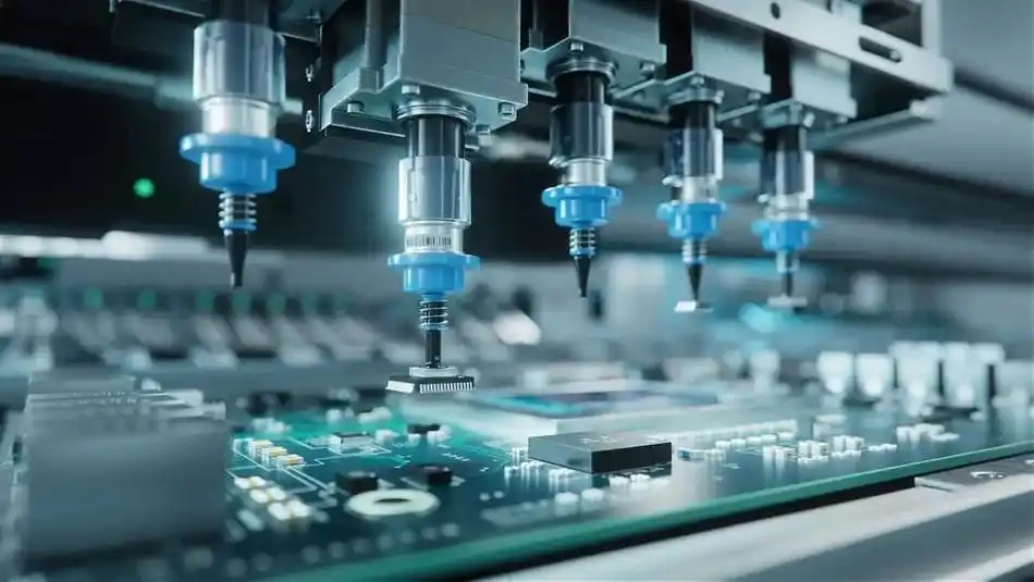
Step 4: SMT Component Pick and Place
After paste is printed, the PCB moves into the pick‑and‑place (P&P) machine where SMT components are mounted onto the pasted pads.
In this stage, the factory will:
- Load components into feeders from reels, trays, or tubes
- Program the P&P machine using your centroid file and component library (package size, rotations, pickup locations)
- Use vision systems to correct for slight component or board misalignment
- Place components at high speed and with precise angle and position
Typical components placed by SMT include:
- Resistors, capacitors, inductors (chip size from 1206 down to 01005)
- ICs: QFP, QFN, BGA, CSP, SOIC, and many others
- Connectors and shields designed for SMT
- LEDs and other SMD devices
Practical tips for customers:
- Make sure designators in the BOM and the centroid file match exactly
- Mark polarity and pin‑1 clearly on the silkscreen and assembly drawing, especially for diodes, electrolytic capacitors, and ICs
- Avoid placing very tall mechanical parts in SMT if they can interfere with reflow or later THT processes
Step 5: Reflow Soldering
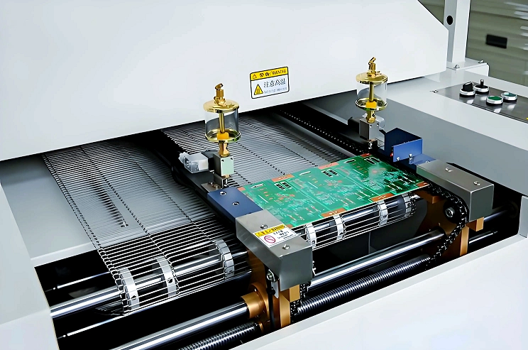
Once SMT components are placed, the board passes through a reflow oven where the solder paste melts and forms permanent joints. The quality of the reflow profile directly affects joint strength, voiding, and risk of damage to components.
A typical reflow process includes:
- Preheat zone: Gradually raises the board temperature to avoid thermal shock and activate flux
- Soak zone: Keeps the board at a moderate temperature to equalize heat across the board and drive off volatiles
- Reflow zone: Brings the solder above its melting point for a short time to create proper wetting and fillets
- Cooling zone: Controlled cooling to solidify joints without excessive stress or micro‑cracks
Common reflow problems:
- Tombstoning of small passives due to uneven wetting or unbalanced pad sizes
- Solder balls from aggressive heating or paste issues
- BGA voids or hidden opens under large packages
As a customer, you should:
- Check that your partner has separate leaded and lead‑free profiles if required
- Confirm they log and control oven profiles, especially for complex or heavy boards
- Discuss any special components with narrow temperature limits (for example, certain connectors or sensors)
Step 6: AOI Inspection and X‑ray for Hidden Joints
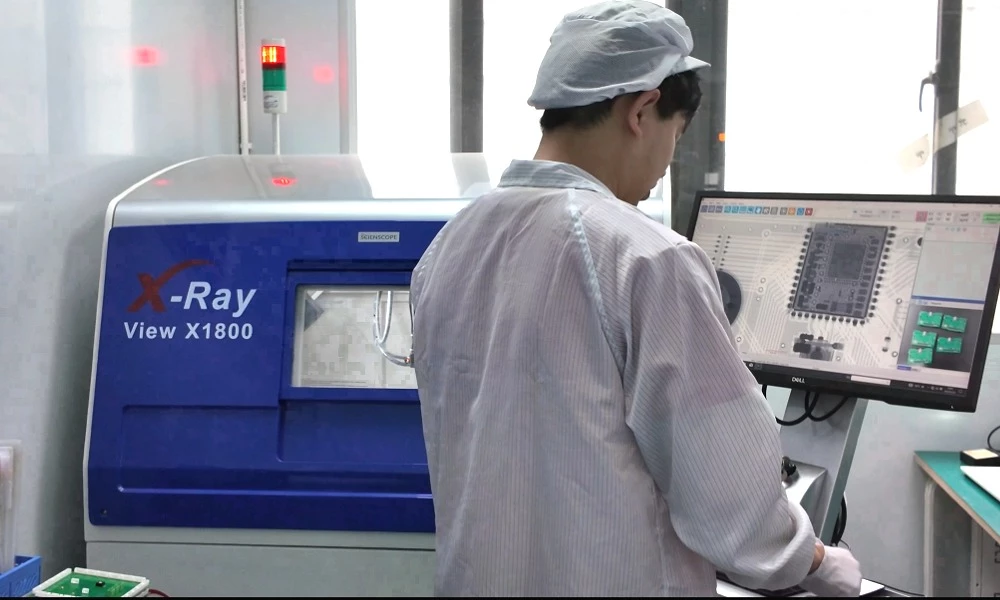
After reflow, most boards go through Automated Optical Inspection (AOI) to visually verify component presence, polarity, offsets, and solder joint quality. For BGA and some QFN packages, X‑ray inspection is used because their joints are not visible from the outside.
AOI typically checks for:
- Missing components, wrong components, or extra components
- Misalignment, rotation errors, and polarity mistakes
- Solder bridges between pins
- Insufficient or excessive solder on visible joints

X‑ray inspection focuses on:
- BGA ball alignment
- Voids inside solder balls
- Shorts between internal pads under packages
Practical actions you can take:
- Ask for AOI coverage: which areas and which sides of the board are inspected
- For high‑reliability products, request sample AOI/X‑ray reports for your first article
- Make sure your design includes fiducials and clear polarity marks to help AOI algorithms
Step 7: THT Assembly and Wave / Selective Soldering
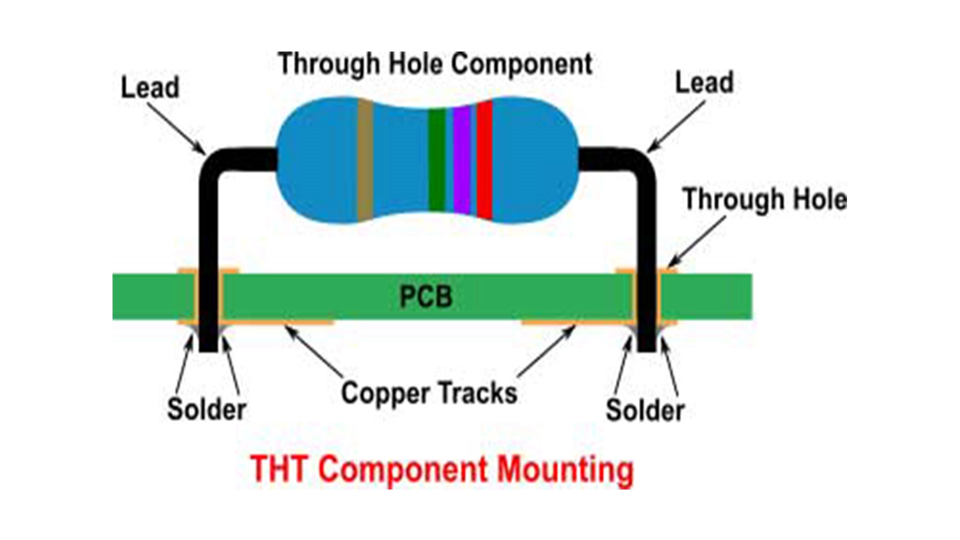
Through-hole technology (THT) is a traditional PCB assembly method where components like resistors, capacitors, and connectors are placed by inserting their leads into drilled holes. These leads are then soldered to pads on the opposite side, creating a strong, mounted mechanical and electrical bond. Unlike SMT, which uses smaller components directly onto the board surface, THT is better for parts that need to handle high stress or heat.
Through‑hole technology (THT) is still widely used for connectors, power devices, large electrolytic capacitors, transformers, and high‑mechanical‑strength parts. In mixed‑technology boards, SMT is normally completed first, and then THT components are inserted.
THT assembly usually involves:
- Manual or automated insertion of through‑hole components into drilled and plated holes
- Wave soldering for boards that can be fully or partially exposed to a solder wave
- Selective soldering for targeted areas or when only a few THT parts exist
- Manual soldering for special or low‑volume cases
Wave soldering:
- The board passes over a wave of molten solder that contacts the underside and solders all exposed leads and pads at once
- It is highly efficient for boards with many THT parts but requires careful design of solder masks and pad layout
Selective soldering:
- A focused mini‑wave solders only specific areas, ideal for mixed SMT/THT boards where you cannot expose all SMT solder joints to the solder wave
THT inspection often uses visual checks, AOI adapted for THT, and sometimes X‑ray for complex assemblies.
As a designer or buyer, you can support good THT results by:
- Ensuring correct hole diameters vs lead sizes and plating thickness
- Avoiding unnecessary copper near THT pads that can steal heat or cause solder bridging
- Defining which components must be hand‑soldered and noting any special requirements (for example, torque on terminal blocks)
Step 8: Cleaning and Conformal Coating (If Needed)
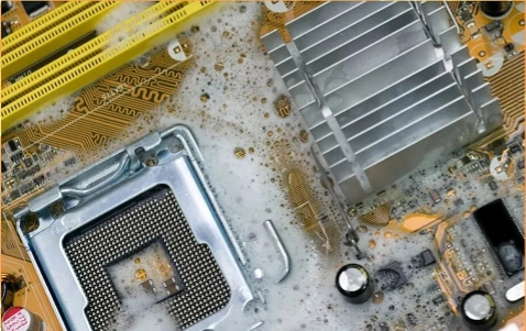
After soldering, some boards require cleaning to remove flux residues, especially if no‑clean flux is not used or if the product operates in harsh environments. Residues can lead to corrosion, leakage currents, or cosmetic issues.
Depending on your requirements, the factory may:
- Use aqueous cleaning with deionized water and detergents
- Use semi‑aqueous or solvent‑based cleaning systems
- Perform ionic contamination testing for critical applications
Conformal coating is a protective polymer layer applied on the assembled board to shield it from moisture, dust, chemicals, and temperature extremes. It is common in industrial control, automotive, outdoor IoT, and navigation systems.
If your project may need cleaning or coating, discuss this early because it impacts:
- Board layout (keep‑out areas, mask openings)
- Choice of flux and solder mask
- Fixtures and masking for coating
Step 9: Electrical and Functional Testing
At this stage, the board has all components soldered and visually inspected, but it still needs to prove that it actually works. Testing is where you validate that the assembly process has produced functional products, not just good‑looking boards.
Common test methods:
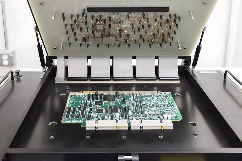
- In‑Circuit Test (ICT): Uses bed‑of‑nails fixtures to probe many nodes and check for opens, shorts, wrong values, and some functional conditions
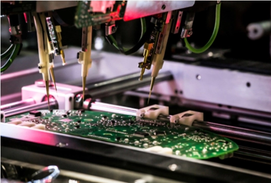
- Flying‑probe test: Uses moving probes and is suitable for lower volumes and when ICT fixtures would be too expensive
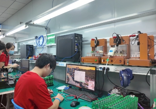
- Functional test (FCT): Powers up the board and runs a test program or script to verify key functions, communication, and performance
As a customer, you play a key role:
- Decide which test strategy makes sense for your volume and risk profile
- Provide test specifications, pass/fail criteria, and any special fixtures or firmware
- Involve your factory early so they can design extra test points and accessible connectors into the PCB
Skipping proper testing may save some unit cost but usually leads to higher field failure rates and returns later.
Step 10: Final Quality Inspection and Packing
Before shipment, boards undergo final checks and are packed for transport.
Typical final steps:
- Visual inspection for cosmetic defects, labeling, and completeness
- Verification against order: PCB revision, quantity, configuration, and any special instructions
- Application of labels, barcodes, or serial numbers as required
- Packing in ESD‑safe bags, foam, or trays, then carton boxes with moisture barriers or desiccant if needed
You should clarify with your partner:
- Packing format (per piece, panel, or full set with accessories)
- Any drop‑test or transport requirements
- Whether they can add your own labels, QR codes, or branding at this stage

Typical PCB Assembly Steps and Customer Responsibilities
The table below summarizes what a professional factory does at each stage and what you, as the customer, should prepare.
| Process Step | What the Factory Does | What You Should Prepare |
|---|---|---|
| Pre‑production & DFM | Check Gerber, BOM, drill files, assembly drawings; confirm manufacturability and panelization. | Complete, consistent Gerber/ODB++, BOM with full MPNs, centroid, assembly notes, test requirements. |
| SMT printing & placement | Design stencil, print solder paste, place SMT components using P&P machines. | Reasonable pad design, clear polarity marks, confirmed substitutes and critical components. |
| Reflow soldering | Set and control oven profile, solder SMT joints, inspect for major defects. | Highlight sensitive components and any special thermal limits. |
| THT insertion & soldering | Insert through‑hole parts, wave/selective/manual soldering, inspect joints. | Correct hole diameters, clear drawings for connectors and mechanical parts. |
| Inspection (AOI/X‑ray) | Run AOI, X‑ray for BGA/QFN, manual checks, rework when needed. | Design fiducials and clear silk orientation, approve inspection criteria. |
| Testing | Execute ICT/flying‑probe/FCT based on plan, log results and failures. | Provide test specs, firmware, fixtures, and definition of pass/fail behavior. |
| Cleaning, coating, packing | Clean boards if required, apply conformal coating, pack in ESD‑safe materials. | State reliability/environment requirements and packing preferences early. |
Use this as a checklist when preparing new projects; it will save time and reduce miscommunication.
SMT vs THT in the PCB Assembly Process
Understanding how SMT and THT fit into the overall assembly flow helps you make better design and sourcing decisions. In modern manufacturing, most boards use a mix of both technologies.
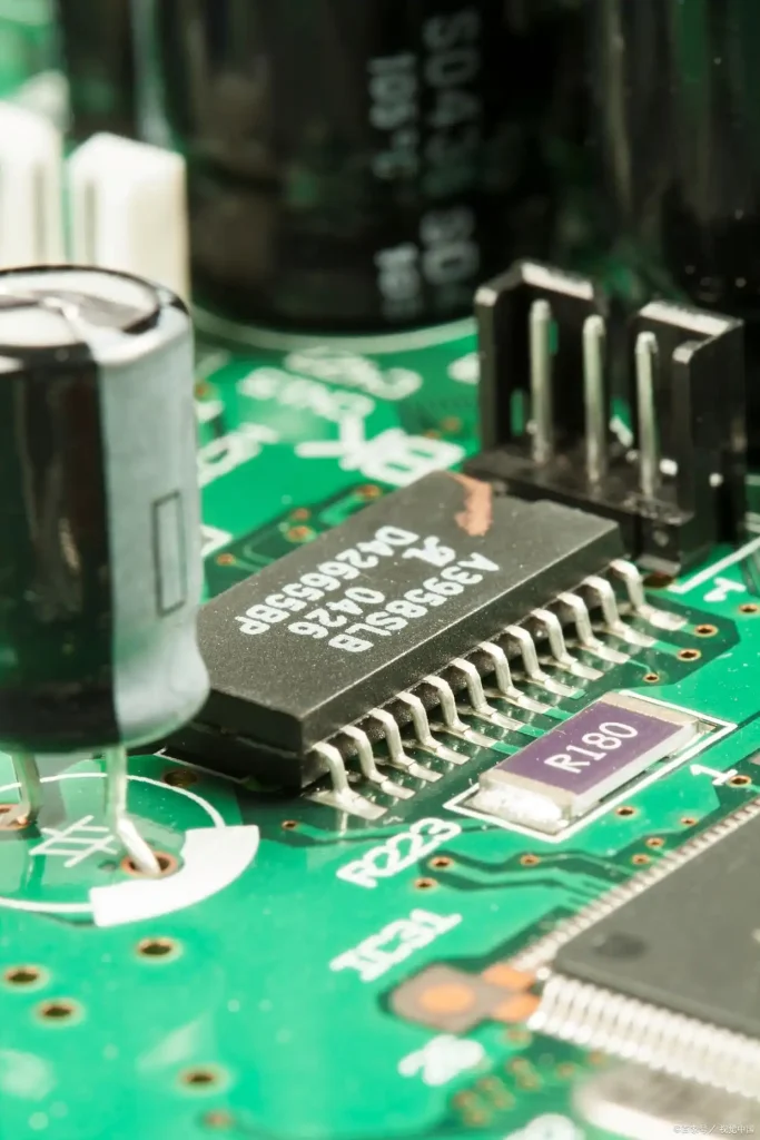
SMT: Surface‑Mount Technology
- Components are mounted directly onto pads on the PCB surface and soldered by reflow
- Very suitable for high‑density, high‑speed, and compact designs
- Enables automated placement at high speed and lower labor cost
Typical flow: solder paste printing → SMT placement → reflow → AOI → (X‑ray for BGAs) → rework if needed.
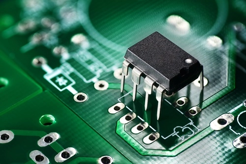
THT: Through‑Hole Technology
- Component leads pass through drilled holes and are soldered on the opposite side of the board
- Offers strong mechanical strength and is favored for high‑current, high‑voltage, or mechanically stressed components
- More labor‑intensive and space‑consuming than SMT
Typical flow: THT insertion → wave/selective/manual soldering → inspection → testing.
For mixed‑technology designs, a common sequence is:
- SMT on side A → reflow
- SMT on side B (if any) → second reflow
- THT insertion → wave/selective/manual soldering → final inspection
As a designer or buyer, try to:
- Keep heavy parts and tall connectors as THT when mechanical strength is critical
- Avoid placing SMT parts too close to THT pads that will see wave soldering unless you plan for selective soldering
- Coordinate early with your assembly partner about which components will be SMT vs THT to optimize cost and quality
How to Prepare for a Smooth PCB Assembly Project?
Even the best factory cannot fix poor documentation or unclear requirements. This section gives you concrete preparation checklists to minimize risk and headaches.
Files and Documentation Checklist
Before requesting a quote or starting production, you should have:
- PCB Gerber/ODB++ with clear layer naming and drill files
- Complete BOM:
- Manufacturer and full MPN for each item
- Package, value, tolerance, voltage/current rating
- Approved alternative parts or “no substitution” notes for critical items
- Pick & Place (centroid) file with X, Y, rotation, and designator
- Assembly drawings (PDF) with:
- Top and bottom views
- Polarity, pin‑1 indicators, and mechanical references
- Notes for special handling (for example, do not wash, height limits)
- Test documents: test points, functional test description, programming instructions if needed
Engineering & Quality Checklist
To reduce surprises during assembly, define in advance:
- Which components are critical (must not be substituted)
- Required standards (for example, IPC‑A‑610 Class 2 or 3)
- Solder alloy preference (leaded vs lead‑free)
- Cleaning requirements (no‑clean, wash, or specific ionic cleanliness levels)
- Conformal coating areas and keep‑out zones if coating will be applied
- Testing level: visual only, electrical, in‑circuit, or full functional test
Logistics & Communication Checklist
Smooth projects depend on clear expectations:
- Target lead time and any fixed milestones (for example, demo, trade show, customer pilot)
- Quantities for prototype, pilot, and mass production phases
- Responsibility for component sourcing:
- Turnkey (factory sources everything)
- Consigned (you provide all components)
- Hybrid (factory sources common parts, you supply special ICs)
- Main communication channel (email, collaboration tool) and time‑zone overlap windows
Sending this information clearly at the start allows your assembly partner to plan lines, material purchasing, and testing resources correctly.

Common Problems in the PCB Assembly Process and How to Avoid Them
Even with good PCB design and manufacturing, issues can still appear during PCB assembly; understanding the common ones lets you design them out or catch them early.
Problem 1: Solder Bridges and Shorts
Bridging happens when too many solder links are adjacent pads, especially on fine‑pitch ICs.
How to reduce risk:
- Use recommended pad sizes and spacing for your pitch
- Ensure proper stencil design with aperture reductions for fine‑pitch pads
- Avoid placing solder mask‑defined pads for very small gaps unless guided by IPC rules
- Request AOI coverage for all fine‑pitch components
Problem 2: Tombstoning of Small Passives
Tiny resistors and capacitors can stand up on one end during reflow if solder forces are unequal.
Prevention tips:
- Keep pad sizes and thermal masses balanced on both sides of the component
- Avoid large copper pours connected to only one side of a very small component
- Use reflow profiles recommended for your paste and board construction
Problem 3: Wrong Component Orientation or Polarity
Diodes, polarized capacitors, and ICs assembled in the wrong orientation cause immediate failures and can be hard to debug later.
Avoid this by:
- Using clear silkscreen markings for polarity, pin‑1, and orientation
- Including orientation notes in assembly drawings
- Checking the first articles carefully before mass production
Problem 4: Poor THT Solder Joints
THT joints can suffer from insufficient wetting, voids, or intermittent connections.
To improve THT quality:
- Ensure hole diameters and plating are appropriate for lead size
- Avoid excessive thermal mass around THT pads that makes soldering difficult
- Define any special soldering requirements, especially for high‑current or safety‑critical connections
Problem 5: Test Coverage Gaps
Boards may pass visual inspection but still fail in the field because the test strategy was weak.
Mitigation:
- Plan test points and test strategy during design, not after layout is complete
- For volume production, consider ICT or well‑designed flying‑probe plus functional test
- Define pass/fail criteria clearly and share expected failure modes with your assembly partner
Building awareness of these issues and addressing them in design and documentation is one of the most effective ways to improve yield and long‑term reliability.
Working With a One‑Stop PCB Assembly Partner in China
Many OEMs and hardware startups choose Chinese partners for PCB assembly due to cost, capacity, and supply‑chain depth, but success depends on collaboration quality.
Why OEMs Choose China for PCB Assembly?
- Large ecosystem of PCB fabs, assembly houses, and component distributors
- Competitive pricing for both prototypes and mass production
- Flexible capacity for multi‑SKU, low‑to‑medium volume runs
- Experience with global customers and export logistics
However, differences in time zone, language, and expectations can create friction if not managed proactively.
How to Evaluate a PCB Assembly Factory?
When you assess potential partners, look beyond quoting price and consider:
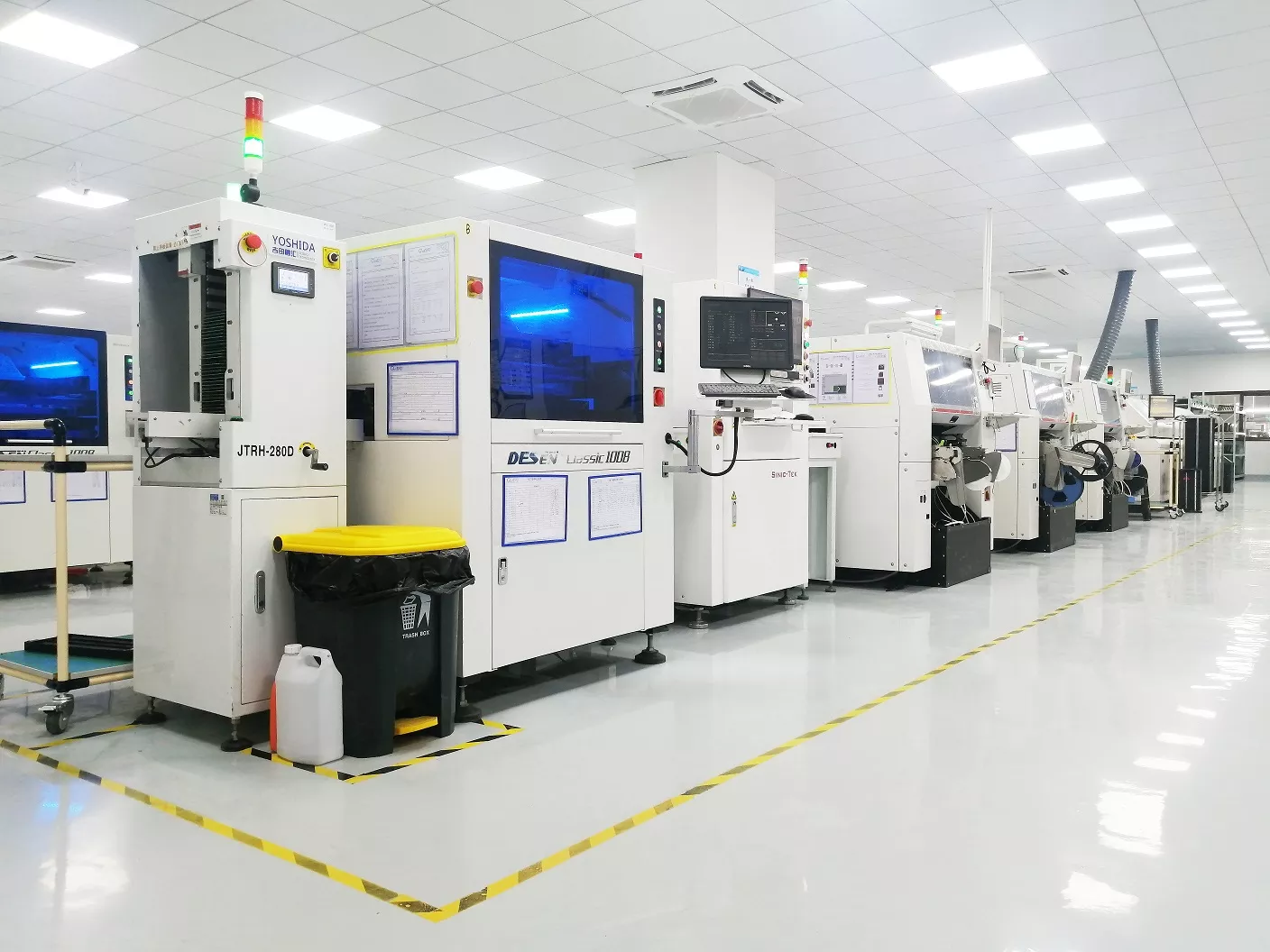
- Process capabilities:
- SMT line configuration, minimum component size, BGA and fine‑pitch experience
- THT, wave, and selective soldering capability
- AOI, X‑ray, SPI, ICT, and functional test availability
- Engineering support:
- Will they perform DFM reviews and suggest improvements?
- Can they help optimize BOM for local supply‑chain cost and availability?
- Quality system:
- Certifications, documented procedures, and traceability for batches and components
- Clear handling of non‑conformities, rework, and corrective actions
You want a partner that acts as an extension of your engineering team, not just a “board stuffing” shop.
How IWDF Solutions Can Support Your PCB Assembly Projects?
As a Shenzhen‑based one‑stop PCB and PCBA provider, IWDF Solutions integrates PCB design, PCB reverse engineering, IC unlocking services, PCB fabrication, and full PCB assembly under one roof. This structure allows IWDF to:
- Start helping from an early stage by reviewing schematics and layouts for DFM/DFT concerns
- Manage both SMT and THT, including complex mixed‑technology boards, industrial and automotive‑grade assemblies
- Provide engineering feedback on BOM choices, suggest local component alternatives where appropriate, and flag high‑risk parts before procurement
For overseas B2B customers, IWDF can:
- Review your Gerber, BOM, and assembly data and highlight manufacturability issues before you commit to tooling and volume builds
- Offer prototype and small‑batch runs with the same process controls used for mass production
- Support different cooperation models: turnkey assembly, consigned parts, or a mix based on your supply chain
The goal is to lower your project risk and shorten the time from first idea to a stable, repeatable PCBA in the field.

FAQs About the PCB Assembly Process
1. What files are required to start the PCB assembly process?
Most assembly houses need at least:
- Gerber/ODB++ files for all copper, solder mask, and silkscreen layers
- Drill files and board outline
- BOM with full manufacturer part numbers and package information
- Pick & Place (centroid) file
- Assembly drawings and any special notes or test requirements
Providing a complete set from day one avoids delays and back‑and‑forth emails.
2. How long does the PCB assembly process take?
Lead time depends on material availability, line loading, and complexity, but a typical pattern is:
- Prototypes: a few days to two weeks after all materials arrive
- Small to medium production: two to four weeks
- High volume or complex, heavily tested boards: longer, especially if special fixtures or certification tests are involved
Discuss your timeline early and factor in time for first article approval.
3. What is the difference between PCB manufacturing and PCB assembly?
PCB manufacturing (fabrication) produces the bare board: copper traces, vias, solder mask, and silkscreen. PCB assembly mounts components onto that board and solder them to create a complete PCBA. You often need both services, but they can be provided by separate suppliers or by a one‑stop partner.
4. Can one supplier handle both SMT and THT processes?
Yes, many professional assembly houses operate SMT lines combined with THT insertion and wave/selective soldering capabilities. If your design includes high‑pin‑count connectors, large capacitors, or high‑current parts, confirm that your supplier can manage mixed‑technology boards and has clear process flows for them.
5. How do you ensure quality during the PCB assembly process?
Quality is controlled by a combination of DFM review, process control, inspection, and testing:
- Upfront DFA/DFM file checks
- Controlled solder paste printing and reflow profiles
- AOI and X‑ray inspection where needed
- Clear workmanship standards (such as IPC‑A‑610)
- Appropriate electrical and functional testing
Ask potential partners about each of these areas and request sample reports if possible.
6. Do I need to supply all components, or can the factory source them?
Most PCB assembly factories can offer:
- Full turnkey: they purchase all parts and manage the supply chain
- Consigned: you provide all components
- Hybrid: they source common passives and standard ICs, while you supply special or sensitive chips
For overseas customers, turnkey or hybrid models usually reduce logistics effort and overall project complexity.
How to Start Your PCB Assembly Project With IWDF Solutions?
If you are planning a new board for your industry or looking to move existing production to China, the most effective first step is to share your technical package for a structured review.
A practical way to begin:
- Send your Gerber/ODB++, BOM, and assembly files plus target quantity and schedule
- Ask for a DFM review, a proposed assembly process (including SMT, THT, and test flow), and a quotation under different lot sizes
- Discuss whether prototypes, pilot runs, and mass production can be planned as a phased roadmap
IWDF Solutions can provide a no‑obligation initial review of your design, identify potential manufacturability or testing risks, and outline a realistic plan from first sample to volume production. This approach allows you to benefit from a full, professional PCB assembly process while keeping control over quality, cost, and time to market.

