

Choosing the wrong multilayer PCB manufacturer costs you months of delays, failed audits, and boards that don’t work in the field. Most buyers only realize this after it happens.
Multilayer PCB manufacturing bonds three or more copper layers with insulating dielectric material under heat and pressure. The full process runs over 30 steps — from DFM review and lamination to via plating and electrical testing. Getting it right requires coordinated decisions from both the design team and the manufacturer, made before a single file is sent.

Most guides describe what happens inside the factory. That matters — but what you decide before sending your files shapes every step that follows. Stack-up configuration, substrate material, and via types must be locked in before production begins; once lamination is complete, those choices cannot be undone. This article covers them in order: what you finalize first, what the factory does next, how to verify quality, how to select the right supplier, and what drives the final price.
What Engineering Decisions Must You Make Before Production Starts?
Sending incomplete or uncoordinated design files is the most common — and most expensive — mistake in multilayer PCB projects. The factory cannot fix a stack-up once the board is laminated.
Three decisions control your board’s signal performance, reliability, and cost before the factory touches a single panel: stack-up configuration, substrate material, and via type. Each one must be coordinated with your manufacturer before layout is finalized — not after.
Stack-Up Design: The Foundation of Signal Integrity
A stack-up defines the sequence of copper layers and dielectric materials inside the finished board. It controls characteristic impedance, EMI shielding, signal return paths, and mechanical stability.
The most common mistake is treating the stack-up as an afterthought. Some PCB design engineers finish the layout, then ask the factory to sort it out. That produces impedance values that miss targets, boards that warp after lamination, and crosstalk that only appears during testing.
The correct sequence is:
- Define signal speed and frequency requirements first
- Agree on impedance targets with the factory
- Get the factory’s standard stack-up options for your layer count
- Build the layout around confirmed dielectric thicknesses — not assumed ones
Here are the most common configurations:
| Layer Count | Typical Layer Sequence | Primary Use Case |
|---|---|---|
| 4-layer | Signal / GND / PWR / Signal | General electronics, basic EMI control |
| 6-layer | Signal / GND / Signal / Signal / PWR / Signal | Improved routing density, digital boards |
| 8-layer | Sig / GND / Sig / PWR / GND / Sig / GND / Sig | High-speed digital, controlled impedance |
| 12+ layers | Alternating signal and reference planes | 5G hardware, AI servers, ADAS modules |
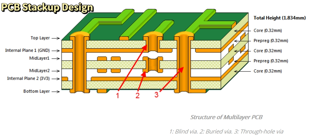
Two rules apply to every stack-up. First, place signal layers adjacent to reference planes — ground or power — to provide the return current path that keeps signals clean. Second, keep the stack-up symmetrical: mirror copper weights and dielectric thicknesses above and below the board’s centerline. Asymmetric boards warp during lamination cooling. Warped boards cause assembly failures.
Controlled impedance is the other reason to coordinate early. Trace width and dielectric thickness together determine impedance. Dielectric thickness is set by the prepreg and core thicknesses your factory actually stocks — it is not freely adjustable. If your calculation assumes a thickness that the factory doesn’t carry, the finished board will miss its impedance target. Most manufacturers hold ±10% impedance tolerance as standard. High-precision factories hold ±5 ohm for values below 50 ohm. Know your signal requirements and match them to the factory’s documented capability before layout begins.
Material Selection: Match the Substrate to the Application
The substrate material determines three things: signal loss at frequency, thermal endurance, and cost. Standard FR-4 handles most applications well. For RF designs, high-temperature environments, or automotive qualification, the wrong material causes real failures — not theoretical ones.
| Material | Dk | Df (Loss Tangent) | Tg | Best Application |
|---|---|---|---|---|
| Standard FR-4 | 4.0–4.8 | ~0.020 | 130–140°C | Consumer electronics, industrial, general-purpose |
| High-Tg FR-4 | 4.2–4.5 | ~0.018 | 170–180°C | Automotive, lead-free assembly, industrial |
| Rogers RO4003C | ~3.38 | ~0.0027 | >280°C | 5G antenna, RF modules, automotive radar |
| Rogers RO3003 | ~3.00 | ~0.001 | >280°C | Aerospace, mmWave (76–81 GHz), satellite systems |
| Polyimide | ~3.5 | ~0.008 | >250°C | Rigid-flex, extreme-temperature environments |
FR-4’s Df of ~0.020 causes measurable signal loss above 1 GHz. For a 5G radio board operating at 28 GHz, or an automotive radar module at 77 GHz, that loss breaks the link budget. Rogers laminates solve this with Df values as low as 0.001 — but they cost significantly more.
A hybrid stack-up is a practical middle ground. Use Rogers or high-frequency material only on the layers that carry RF signals. Use standard FR-4 on all other layers. A 10-layer board for a 5G small cell might carry Rogers RO4003C on layers 1–2 for RF signal paths and high-Tg FR-4 for layers 3–10. This delivers the performance where it is needed without applying a premium material cost to the full board. Not every factory handles hybrid lamination reliably — confirm documented production experience before specifying this approach.
Via Type Selection: Let Routing Requirements Drive the Decision
The via type sets the physical routing space available across the entire board. Through-hole vias are the default and lowest cost. Blind and buried vias enable higher routing density on the same layer count. HDI microvias are required for fine-pitch BGAs below 0.4 mm pitch. The decision should come from actual routing requirements — not default assumptions.
| Via Type | Function | Typical Use Case | Cost Impact |
|---|---|---|---|
| Through-hole via | Passes all layers from top to bottom | Standard routing, through-hole component mounting | Lowest |
| Blind via | Connects an outer layer to one or more inner layers | BGA fan-out, HDI designs | Medium |
| Buried via | Connects inner layers only; invisible from outside | High-density internal routing | Medium-High |
| Stacked microvia | Multiple blind vias stacked vertically | Fine-pitch BGA at <0.4 mm, miniaturized layouts | Highest |
Blind and buried vias require sequential lamination — the board is built in separate lamination, drilling, and plating cycles for each build-up layer. Each additional cycle adds process time and cost. That cost is only justified when routing genuinely cannot be achieved with through-hole vias.
If your design allows standard through-hole routing, use it. Switching from blind vias to through-hole vias — where routing permits — can reduce fabrication cost by 20–40% on a mid-layer-count board.
With these three decisions locked in, the factory has everything it needs to begin production. Here is exactly what happens next.
What Actually Happens During Multilayer PCB Manufacturing?
Once your stack-up is confirmed, your material is specified, and your design files pass DFM review, production begins. The process runs in a fixed sequence. Each step depends on the one before it, and a failure at any stage either scraps the panel or creates a defect that surfaces later.
Step 1: Pre-Production Engineering and DFM Review
Every order starts with CAM (Computer-Aided Manufacturing) engineering. Gerber files, drill data, and fabrication notes are loaded into the factory’s CAM software. An engineer runs a full Design Rule Check against the factory’s real process capabilities.
DFM checks cover: minimum trace width and spacing (standard: 4/4 mil; advanced: 3/3 mil), via sizes, pad dimensions, annular ring requirements (minimum 3 mil), board thickness-to-drill-diameter aspect ratio (must stay below 10:1 for reliable plating), and controlled impedance targets against the actual stack-up.
A defect caught here costs nothing to fix. The same defect found after lamination means scrapping an entire panel. This step is where manufacturing risk is reduced to near zero — or transferred to the buyer if it is skipped.
Step 2:Inner Layer Imaging and Etching
With DFM approved, inner copper cores are cleaned and coated with light-sensitive dry-film photoresist. The circuit pattern is transferred using one of two methods.
Laser Direct Imaging (LDI) writes the circuit directly from digital Gerber data using a computer-controlled laser. No physical film mask is needed. LDI provides higher registration accuracy and handles fine-pitch designs more reliably than conventional UV exposure.
UV exposure with a phototool aligns a physical film mask with the panel and exposes it to UV light. Reliable for standard line widths of 4 mil and above.
After exposure and development, the panel enters the etching line. Chemical etchant removes the exposed copper. The copper under hardened resist stays intact. After etching, the remaining resist is stripped — leaving the finished inner layer traces. Advanced factories achieve line widths as narrow as 2.7 mil. Standard production runs at 4–5 mil for a consistent yield.

Step 3:Inner Layer AOI Inspection
Before any layer is permanently sealed inside the board, it passes through Automated Optical Inspection (AOI). High-resolution cameras scan the full panel and compare the result against the original Gerber data. The system detects shorts, opens, missing copper, and dimensional errors.
If a defect is found, the panel is scrapped. Inner layers cannot be repaired after this step — and they cannot be corrected at all once lamination is complete. A factory that allows “track welding” repairs on inner layers is a factory to avoid. This step is a non-negotiable quality gate.

Step 4:Oxide Treatment
Immediately after AOI, inner layer copper surfaces receive a brown or black oxide treatment. This chemistry micro-roughens the copper surface at the microscopic level. The texture gives the prepreg resin something to grip during lamination. Without it, the bond strength between copper and dielectric weakens under thermal cycling — and delamination follows over the product’s service life.
Step 5:Stack-Up Assembly and Lamination
The prepared inner layer cores, prepreg sheets, and outer copper foils are stacked in the exact sequence defined in the fabrication specification. The assembled stack enters a lamination press at approximately 180°C and up to 500 psi (35 bar). The prepreg resin flows, fills all gaps between layers, and cures into a single solid panel. A cold press cycle follows to relieve internal stress and prevent warping.
Registration accuracy during lamination separates factories from each other. Even a small layer-to-layer misalignment disrupts signal paths, shifts impedance values, and can break via connections entirely. After lamination, X-ray equipment verifies inner layer registration before drilling begins.
Step 6:Drilling and Via Formation
With lamination complete, holes are drilled for electrical connections between layers and for component mounting.
Mechanical drilling uses CNC machines guided by X-ray registration of inner layer targets. Via diameters range from 0.2 mm to 0.5 mm, with positional accuracy within ±0.05 mm.
Laser drilling creates microvias at 0.076–0.1 mm (3–4 mil) for blind via structures in HDI designs. It is required for via-in-pad on fine-pitch BGAs.
After drilling, a desmear process removes resin residue from the hole walls. Clean walls are essential for copper adhesion in the plating step that follows directly.

Step 7:Electroless Copper Deposition (PTH)
Drilled hole walls are fiberglass and resin — non-conductive. A copper seed layer must be deposited chemically before any electrical plating can occur.
A palladium catalyst first activates the hole wall surfaces. The panel then enters an electroless copper bath, where an autocatalytic reaction deposits a uniform 0.5–1.0 µm copper layer on all surfaces, including hole walls. A follow-up electrolytic cycle builds this to 5–8 µm, preparing the surface for pattern plating.
If this step produces uneven coverage or voids, the via fails. Every signal, power, and ground connection that relies on that via fails with it.
Step 8:Outer Layer Imaging and Pattern Plating
Outer layer imaging follows the same photoresist and exposure process as inner layers. After imaging and development, pattern plating electrodeposits additional copper into the circuit traces and via barrels, building total copper thickness to 25–35 µm. A tin layer protects the plated copper during outer layer etching. After resist strip and final copper etch, the tin is chemically removed — leaving the finished outer layer circuit.
IPC Class 2 requires a minimum of 20 µm copper in plated through-holes. IPC Class 3 requires 25 µm. For medical, automotive, and aerospace applications, always specify Class 3. That extra 5 µm directly improves thermal fatigue resistance under repeated temperature cycling — and it is the difference between a 5-year service life and a field failure at year two.

Step 9:Solder Mask, Surface Finish, Silkscreen, and Profiling
With the copper circuit complete, the board moves through four finishing steps in sequence.
Solder mask is applied across the full board surface and opened at the solder pads using a photolithographic process. It prevents solder bridging during assembly and protects copper traces from corrosion. Available in green, black, blue, red, white, and other colors in matte or glossy finishes.
Surface finish is applied to exposed copper pads to protect solderability and prevent oxidation. The right finish depends on your assembly process and reliability requirements:
| Surface Finish | Shelf Life | Coplanarity | Best For |
|---|---|---|---|
| HASL (Lead-Free) | 12+ months | Moderate | Standard assemblies, cost-sensitive designs |
| ENIG | 12+ months | Excellent | Fine-pitch components, wire bonding, BGA |
| OSP | 6 months | Excellent | Low-cost, short lead-time production |
| Immersion Silver | 6–12 months | Excellent | High-frequency, RF applications |
| Immersion Tin | 6 months | Good | Press-fit connectors |
| Hard Gold / Flash Gold | 12+ months | Excellent | Edge connectors, high-wear contacts, gold fingers |
| ENEPIG | 12+ months | Excellent | Mixed requirements: wire bonding + soldering |
Silkscreen prints component designators, logos, and revision marks and UV-cures them onto the surface. Profiling uses CNC routing, V-scoring, or punching to separate individual boards from the manufacturing panel.

Step 10:Electrical Testing and Final Inspection
Every board goes through 100% electrical testing. Flying probe testing is used for prototypes and small batches — no custom fixture is needed. Bed-of-nails fixture testing is used for high-volume production for faster throughput. Both methods verify that every net is continuous and that no two nets are shortened together.
Impedance test coupons on the panel margin are measured against the fabrication specification. Boards that fall outside tolerance are rejected before final inspection.
Final visual and automated inspection follows IPC-A-600 acceptability criteria. Boards are then packaged with desiccants, humidity indicator cards, and vacuum-sealed anti-static bags. This protects solderability during international shipping — a step skipped by lower-tier suppliers, but one that matters significantly for boards stored weeks or months before assembly.

What Quality Standards Should Your Multilayer PCB Manufacturer Meet?
Any supplier can claim quality. Standards give you something concrete to verify — and a clear basis for rejection when a shipment doesn’t meet spec.
The IPC framework defines global quality benchmarks for multilayer PCBs. Industry certifications add regulatory requirements for automotive, medical, and aerospace applications. Both matter. A factory with ISO 9001 but no IPC Class 3 production experience is not the right partner for a medical device or automotive safety module.
IPC Standards That Define Multilayer PCB Quality
| Standard | What It Covers | How Buyers Use It |
|---|---|---|
| IPC-2221 | Design rules: spacing, conductor sizing, material requirements | Confirms the design meets baseline fabrication requirements |
| IPC-6012 | Qualification and performance for rigid PCBs across Class 1, 2, and 3 | Sets copper plating minimums, hole quality, and electrical performance acceptance criteria |
| IPC-A-600 | Visual acceptability criteria for bare PCBs | Defines acceptable vs. rejectable surface conditions, conductor patterns, and hole quality |
| IPC-TM-650 | Standardized test methods: peel strength, thermal stress, ionic contamination | Specifies how quality is measured and verified in production |
The Class 2 vs. Class 3 distinction is not abstract. It defines specific minimums that affect field reliability:
- IPC Class 2 — Minimum 20 µm copper in plated through-holes. Sufficient for most industrial and commercial electronics.
- IPC Class 3 — Minimum 25 µm copper in plated through-holes. Required for medical implants, aerospace avionics, and automotive safety electronics.
If your product operates in a safety-critical or high-reliability environment, specify Class 3 explicitly and confirm the factory regularly produces to that standard — not just occasionally on special orders.
Industry Certifications: What to Require and How to Verify
| Certification | Applies To | How to Verify |
|---|---|---|
| ISO 9001:2015 | All industries — quality management baseline | Check certificate number via issuing body’s public database (SGS, TÜV, Bureau Veritas) |
| IATF 16949 | Automotive PCB supply chains | Required for any automotive-grade board; verify certificate scope covers PCB fabrication |
| ISO 13485 | Medical device manufacturing | Required for healthcare applications; scope must cover PCB production specifically |
| UL Certification | North American and European OEMs | Verify UL listing number at ul.com/database |
| RoHS / REACH | All export markets | Confirm current compliance reports, not outdated declarations |
One practical warning: always verify certificate numbers directly through the issuing body’s public database. A logo on a website proves nothing. Ask for the certificate document, check the certificate number, confirm the expiry date, and confirm the scope covers PCB fabrication — not just a parent company’s general operations.
How Do You Choose the Right Multilayer PCB Manufacturer in China?
Shenzhen alone has hundreds of PCB factories. Most buyers don’t struggle to find a supplier. They struggle to tell a reliable one from an unreliable one before it’s too late.
Price is a secondary filter. A supplier who charges 15% more but catches a DFM issue before production saves far more in rework, delays, and failed units than the cheaper alternative who ships defective boards and argues about liability afterward.
Capabilities Checklist: Fill This In Before You Request a Quote
Request a written capability matrix from any factory you are considering. Match it against your design requirements before engaging further:
| Parameter | Standard Capability | Advanced Capability |
|---|---|---|
| Layer count | 4–20 layers | 40–50+ layers |
| Minimum line/space | 4/4 mil | 2.7/2.7 mil or finer |
| Minimum drill size | 0.2 mm mechanical | 0.076 mm laser |
| Board thickness range | 0.4–3.2 mm | 0.2–6.0 mm |
| Copper weight | 0.5–3 oz | 0.5–10 oz |
| Impedance tolerance | ±10% | ±5 ohm for values below 50 ohm |
| Via types | Through-hole only | Blind, buried, stacked microvias |
| Materials supported | FR-4 | Rogers, PTFE, polyimide, hybrid lamination |
| Surface finishes | HASL, ENIG | Full range including ENEPIG, hard gold |
| Maximum board size | 500 × 400 mm | 1100 × 500 mm |
Any gap between your requirements and the factory’s stated capabilities is a production risk. Do not assume a factory can stretch beyond its documented process limits on your order.

One-Stop Service: Why It Matters for International Buyers
Managing separate suppliers for PCB design, fabrication, and assembly across multiple time zones creates coordination overhead that adds weeks and introduces accountability gaps. When a defect appears, no single vendor owns it — and multi-party disputes are costly to resolve.
A true one-stop service partner covers the full product journey:
- PCB Design — Schematic capture, layout, stack-up optimization, and signal integrity analysis using professional EDA tools
- PCB Reverse Engineering and PCB Cloning — Converting a physical board into a complete production package: Gerber files, BOM, and schematic diagrams. This is essential when original design files are lost, when legacy equipment needs to be replicated, or when a reference design requires analysis and reproduction
- PCB Fabrication — Prototype through mass production, multilayer and HDI capability
- PCBA (Assembly) — SMT and through-hole assembly, in-house component sourcing, reflow and wave soldering
- Testing and Quality Assurance — AOI, X-ray inspection for BGA and QFN packages, ICT, and functional test
When these services are under one roof, there is single-point accountability. If a defect appears, there is one team to call — not a three-way disagreement between your design house, fabricator, and assembly partner.
China vs. Other Regions: A Practical Comparison for B2B Buyers
| Factor | China (Shenzhen) | North America / Europe |
|---|---|---|
| Per-unit cost | 20–50% lower for comparable quality | Higher due to labor and operating costs |
| Prototype lead time | 5–10 working days | 10–20 working days |
| Supply chain depth | Deep — laminates, chemicals, and components nearby | Largely dependent on Asian material supply |
| Certification availability | ISO 9001, IATF 16949, ISO 13485, UL — all available | Same |
| English-language engineering support | Varies — verify before committing | Generally strong |
| IP protection | Requires explicit written NDA; enforce proactively | Stronger legal framework by default |
For most international B2B buyers, China offers the strongest combination of cost, speed, and technical depth for multilayer PCB manufacturing. The risks — IP protection and communication quality — are manageable with the right supplier, properly structured NDA agreements, and clear written technical specifications.
What Drives the Cost of Multilayer PCB Manufacturing?
Most engineers underestimate how much design decisions control the final price. Layer count is the dominant cost driver. Material, via type, and copper weight follow. Understanding the levers lets you make design trade-offs with real budget impact — rather than being surprised by a quote.
Cost Driver Breakdown
| Cost Driver | Lower Cost Direction | Higher Cost Direction | Practical Optimization |
|---|---|---|---|
| Layer count | 4–6 layers | 20+ layers | Minimize layer count; maximize routing density per layer |
| Material | Standard FR-4 | Rogers, PTFE, polyimide | Use specialty material only on layers where performance requires it |
| Via type | Through-hole only | Blind, buried, stacked microvias | Avoid blind/buried vias if standard through-hole routing is feasible |
| Copper weight | 1 oz standard | 4 oz+ heavy copper | Match copper weight to actual current and thermal requirements |
| Surface finish | HASL, OSP | ENIG, ENEPIG, hard gold | Choose based on assembly process — not aesthetics |
| Board size and shape | Standard panel-efficient shapes | Non-standard shapes, thin boards | Design for standard panel sizes to maximize panelization efficiency |
| Impedance control | Not required | Tight tolerance with test coupons | Specify controlled impedance only on signal layers that genuinely need it |
| Volume | 1–10 prototype pieces | 1,000+ production units | Plan production volumes early — per-unit cost drops significantly at scale |
One practical example: switching from blind vias to through-hole vias — when routing permits — can reduce fabrication cost by 20–40% on a mid-layer-count board. Present both routing approaches to your manufacturer before locking in the stack-up. Get pricing on both options. The difference is often larger than engineers expect.
A second practical note on volume: a 4-layer prototype may cost $80–$200 for a small batch. The same board at 1,000-unit production can fall below $5 per piece. This cost structure means planning for production volume at the prototype stage — even if it’s just an estimate — gives the factory information that affects how they quote the tooling and setup costs.

Frequently Asked Questions
What is multilayer PCB manufacturing?
Multilayer PCB manufacturing is the process of fabricating a printed circuit board with three or more copper layers separated by insulating dielectric material. The layers are laminated together under heat and pressure. The full process includes DFM review, inner layer imaging and etching, AOI inspection, oxide treatment, lamination, drilling, electroless copper deposition, outer layer plating, solder mask and surface finish application, electrical testing, and final inspection.
How many layers does a multilayer PCB typically have?
Most commercial multilayer PCBs use 4 to 16 layers. Consumer electronics commonly use 4–8 layers. High-speed digital boards, 5G infrastructure hardware, and AI server boards use 12–24 layers. Specialized aerospace and defense applications can exceed 40–50 layers. The correct layer count is always the minimum needed to meet routing density and signal integrity requirements — adding layers beyond that only increases cost.
What is the difference between a 4-layer and an 8-layer PCB?
A 4-layer board has two inner layers — typically one ground plane and one power plane — sandwiched between two outer signal layers. An 8-layer board adds more signal layers and additional reference planes. The extra layers improve routing density, provide better EMI shielding, and support more controlled impedance signal paths. The trade-off is higher fabrication cost and longer lead time.
What is controlled impedance and why does it matter?
Controlled impedance means the trace width and dielectric thickness are precisely set so that signal traces on the board present a specific characteristic impedance — most commonly 50 ohm for single-ended signals or 100 ohm for differential pairs. This matters for high-speed digital signals (USB, PCIe, DDR), RF signals, and any line where signal reflection or loss would cause errors. The fabricator must coordinate with the designer on the exact stack-up to hit the target value reliably.
What is HDI in multilayer PCB manufacturing?
HDI stands for High-Density Interconnect. HDI boards use laser-drilled microvias (0.076–0.1 mm diameter), blind and buried vias, and fine line/space (2.7 mil or less) to achieve higher routing density than standard multilayer boards. HDI is required for fine-pitch BGA components at 0.4 mm pitch or below. It is widely used in smartphones, 5G modules, wearable devices, and miniaturized medical electronics.
What certifications should a multilayer PCB manufacturer hold?
At a minimum, ISO 9001:2015 for quality management. For automotive projects, IATF 16949 is required. For medical devices, ISO 13485 is required. UL certification is expected by most North American and European OEMs. IPC-6012 Class 3 compliance should be verified for any safety-critical application. Always verify certificate numbers directly through the issuing body’s database — not from the supplier’s marketing materials alone.
What is the difference between PCB fabrication and PCBA?
PCB fabrication produces the bare circuit board — the laminated, drilled, plated, and finished substrate with no components on it. PCBA (Printed Circuit Board Assembly) is the next step: components are placed and soldered onto the fabricated board. A one-stop service provider handles both under the same roof, which shortens total lead time and creates single-point accountability for quality.
What is PCB reverse engineering and when is it needed?
PCB reverse engineering converts a physical circuit board — with no original design files available — into a complete set of production documents: Gerber files, schematic diagrams, and a bill of materials. It is used when original design files are lost or never existed, when legacy equipment must be replicated for repair or upgrade, or when a reference design needs to be analyzed. A reliable PCB reverse engineering service reproduces the original design accurately and provides production-ready files that can be sent directly to fabrication.
How long does multilayer PCB manufacturing take?
Standard prototypes: 5–10 working days. Express prototypes: 2–4 working days. Small-to-medium production batches: 7–15 working days. High-layer-count boards with HDI features or specialty materials: 15–20 working days. Mass production at high volume: negotiate lead time based on order size and factory capacity. These timelines refer to fabrication only — PCBA adds additional time for sourcing, assembly, and testing.
How do I send files to a multilayer PCB manufacturer?
Provide Gerber files in RS-274X format, an Excellon drill file, a complete stack-up drawing with layer sequence and dielectric thicknesses, controlled impedance specifications (target values, tolerance, and reference layers), solder mask color and surface finish selection, board outline and dimensions, and any special fabrication notes. For PCBA orders, also include a bill of materials (BOM) and a component placement file (CPL or XY file). The more complete and unambiguous your documentation, the faster the DFM review and the fewer back-and-forth clarifications before production begins.
The Supplier You Choose Decides More Than You Think
Every decision that shapes your board’s performance — stack-up, material, via type — is made before production starts. Once lamination is complete, nothing can be undone. The right multilayer PCB manufacturer catches problems at that stage, not after shipment.
At IWDF Solutions, we offer a complete one-stop service from PCB design and PCB reverse engineering through multilayer PCB manufacturing and PCBA production in Shenzhen. Every order starts with a DFM review. Send us your requirements today.

