

Global manufacturers increasingly face complex challenges in delivering industrial control systems that operate reliably across unpredictable environments and extended lifecycles. Industrial control PCB assembly represents far more than standard electronics manufacturing—it demands precision engineering, specialized expertise, and an integrated approach that spans design optimization, component sourcing, rigorous testing, and long-term support. This comprehensive guide explores what distinguishes industrial control PCBA from conventional assembly, the technical and operational requirements that drive manufacturing decisions, and how to identify and partner with a manufacturer capable of delivering solutions that meet the exacting standards of modern automation and control applications.
What Is Industrial Control PCB Assembly?
What Is Industrial Control PCB Assembly? A Beginner’s Guide
At the heart of every modern factory, assembly line, or automated system is a specialized kind of brain: the Industrial Control PCB (Printed Circuit Board).
Think of it like the motherboard inside your computer, but built for much tougher challenges. While your laptop or phone works in relatively safe, indoor environments, industrial control boards are the heroes behind the scenes in factories. They have to keep working perfectly despite heat, cold, vibrations, dust, and electrical interference.
In short, an Industrial Control PCB is a powerful, durable circuit board that makes automated equipment smart. It controls machines, reads sensor data, manages power, and ensures everything runs smoothly and safely.
From PCB to PCBA: What Does “Assembly” Mean?
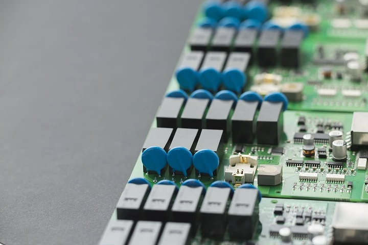
A blank PCB starts as just a board with copper pathways. Industrial Control PCB Assembly (PCBA) is the comprehensive process of transforming a bare board into a fully functional electronic control module.
Here’s what that involves in simpler terms:
- Making the Tough Board: First, the board itself is fabricated using strong, durable materials designed to withstand stress and heat.
- Adding the Components: Next, all the tiny electronic components (chips, resistors, connectors, etc.) are precisely placed onto the board and soldered into place. This requires high-precision machines and expert skill.
- Thorough Testing & Protection: This is the most critical part for the industry. The assembled board undergoes rigorous testing to make sure it works flawlessly. It’s also often coated with a protective layer to guard against moisture, dust, and corrosion.
- Programming & Integration: Finally, the software or firmware is loaded onto it, and it’s integrated into a protective case or the larger machine system.
Why Choose a “One-Stop” PCBA Solution?
For businesses building automation systems, managing all these different steps—design, sourcing parts, assembly, testing—with multiple vendors is complex and risky.
A true one-stop PCBA service handles everything from start to finish:
- Design & Planning Advice: Helping you design a reliable board from the start.
- Sourcing Trusted Parts: Procuring high-quality, traceable components.
- Precision Manufacturing: Assembling your board with advanced equipment.
- Rigorous Reliability Testing: Ensuring it will last in real-world conditions.
- Final Programming & Support: Delivering a fully functional module ready to install.
This approach saves you time, reduces hassle, minimizes errors, and gives you a single point of responsibility, ensuring you get a reliable, high-quality control system for your automation needs. Industrial Control PCBA is about building tough, smart electronic brains for machines. A one-stop service means you get a trusted partner to build, test, and deliver that complete “brain” ready to power your automated system reliably.
Typical Industrial Control Applications
Industrial control PCBs serve distinct application categories, each introducing unique environmental and reliability demands:
Programmable Logic Controllers (PLCs) and Remote I/O Modules form the foundation of discrete manufacturing systems and conveyor networks. These devices process hundreds of digital and analog input signals, execute complex logic sequences in real-time, and drive output actuators. The assembly requirements demand multi-layer stackups with isolated ground planes, high-current traces for relay driving circuits, and precise impedance control for communication networks.
Variable Frequency Drives (VFDs) and Servo Motor Drivers control rotational speed and position in pumps, compressors, and machine tools. These applications require power electronics boards managing hundreds of watts or kilowatts through high-power semiconductor devices. The PCBA manufacturing must address thermal management challenges, high-voltage isolation requirements, and robust current sensing architectures that survive motor fault conditions.
Industrial Automation Gateway and Protocol Converters enable communication between legacy equipment using Modbus or Profibus protocols and modern IT infrastructure supporting Ethernet, 4G/5G, and cloud connectivity. These devices operate in distributed locations with limited maintenance access, demanding exceptional reliability over 10-15 year lifecycles and tolerance for power supply variations.
Robot Control Systems and Motion Controllers guide precision positioning in collaborative manufacturing and assembly environments. These applications require deterministic real-time processing, often incorporating multiple processor cores, memory hierarchies, and specialized motion computation accelerators.
Industrial Power Supplies, Uninterruptible Power Supplies (UPS), and Charging Infrastructure deliver stable DC power to critical factory systems or manage rapid energy storage and conversion cycles. These assemblies incorporate high-power magnetics, complex isolated feedback networks, and protection circuitry that must withstand sustained electrical stress.
Industrial HMI Touchscreen Panels and Smart Sensors provide operator interfaces and distributed data collection. While often featuring consumer-grade display technology, the underlying control and communication electronics require industrial-grade reliability and environmental protection.
Each application class introduces specific environmental exposure patterns: PLC systems tolerate moderate temperature ranges but demand immunity to electrical transients from motor switching; VFD boards must dissipate substantial heat while managing voltage stresses up to 1200V; wireless gateway devices face thermal stress from continuous operation in harsh outdoor environments. Effective PCBA design and manufacturing must anticipate these diverse operational contexts during component selection, circuit layout, and production process optimization.

Key Requirements of Industrial Control PCB Assembly
High Reliability and Long Lifecycle Expectations
Industrial control systems represent substantial capital investments for manufacturing facilities. Unlike consumer products with three to five year product cycles, industrial control equipment frequently remains in service for 10-15 years or longer. Extended service life creates unique procurement and manufacturing challenges. Component obsolescence becomes inevitable—semiconductor manufacturers discontinue product lines, passive component suppliers consolidate or exit market segments, and connector manufacturers modify mechanical or electrical specifications.
Successful industrial control PCBA manufacturers establish component lifecycle management procedures that begin during the design phase. This includes second-sourcing strategies that identify qualified alternative devices meeting identical electrical and mechanical specifications. During manufacturing, traceability systems must track component batch codes, manufacturing dates, and supplier documentation. For long-lifecycle projects, manufacturers should maintain component inventory buffers or establish agreements with distributors to secure allocations of legacy components as production volumes decline.
Manufacturing facilities supporting industrial control applications typically maintain ISO 9001 certification frameworks and demonstrate familiarity with industry-specific standards including IPC-A-610 Class 2 and Class 3 acceptability criteria. Automotive-tier applications may require IATF 16949 compliance. Environmental compliance standards including RoHS and REACH restrict hazardous material usage. Some applications in regulated industries—pharmaceutical manufacturing equipment, medical devices, aerospace systems—demand additional certifications or audit compliance.
Design Considerations for Industrial Control PCBs
Industrial control PCB design must solve challenges from electrical noise, heat, and physical stress that are far more severe than in consumer electronics. Understanding these factors helps in evaluating a design’s readiness for the demanding factory environment before manufacturing begins.
1. Electromagnetic Compatibility (EMC) and Interference (EMI)
The Core Issue: Industrial facilities contain numerous high-power switching devices. Industrial equipment like motor drives and welders generates broadband electromagnetic noise. This can contaminate power supplies and signals, causing malfunctions. The design must ensure reliable operation amidst this interference.
Key Design Strategies:
- PCB Layer Stackup: Using dedicated ground and power planes inside the board creates low-impedance return paths. This contains signals and minimizes radiated emissions.
- Controlled Signal Routing: Communication lines (Ethernet, CAN bus) are routed as differential pairs with matched trace lengths and controlled impedance. This makes them resistant to external noise.
- Shielding & Filtering: Strategic use of filters, shields, and careful component placement prevents noise from entering or exiting the board.
2. Power Distribution & Integrity
The Core Issue: The board needs stable, clean voltage levels for different components, even during power transients common in industrial settings.
Key Design Strategies:
- Layered Energy Storage: Large capacitors at the power input provide bulk energy storage for supply transients. Many small ceramic capacitors distributed across the board provide high-frequency decoupling for individual ICs.
- Dedicated Power Layers: For boards drawing hundreds of watts, entire PCB layers are dedicated to primary voltage rails (like +24V). This ensures uniform current delivery and minimizes voltage drop.
3. High Current & Thermal Management
The Core Issue: Controlling motors and actuators requires switching high currents (10-50A+), which generates significant heat in power components and traces. This heat must be managed to prevent failure.
Key Design Strategies:
- Heavy Copper Traces: Traces carrying high current are sized based on cross-sectional area (e.g., 1-1.5A per mm²) to limit temperature rise. A 50A circuit may need a trace over 50mm wide.
- Strategic Component Layout: Heat-generating components are placed for optimal airflow and attached to heatsinks. Temperature-sensitive parts are kept away from hot spots.
- Thermal Simulation: Software models predict junction temperatures before manufacturing, validating the cooling design.
4. Protection Against Environmental & Mechanical Stress
The Core Issue: Factories expose boards to moisture, corrosive chemicals, dust, vibration, and thermal cycling, which can lead to corrosion and broken connections.
Key Design Strategies:
- Conformal Coating: A protective polymer layer (e.g., urethane, silicone) is applied over the assembled board to shield against moisture, dust, and corrosion.
- Potting/Encapsulation: For extreme protection, the assembly is encased in epoxy resin. This offers superior defense but makes repairs impossible.
- Mechanical Reinforcement: Solder joints and pads for heavy components (like large connectors or heatsinks) are designed with strain relief in mind. Mounting holes and extra supports stabilize components against vibration and thermal expansion.

Process and Quality Control in Assembly
Manufacturing industrial control PCBAs requires a level of rigor and inspection far beyond that of consumer electronics. Standard assembly facilities often lack the strict process control needed to meet the reliability demands of industrial automation.
The journey to a reliable board involves several critical stages of control:
1. Precision Soldering Process Control
Successful assembly starts with perfectly controlled soldering. This is managed through careful thermal profiling.
- Reflow Soldering: The entire board is heated in an oven. The temperature profile must be precise—hot enough to form strong solder joints but not so hot that it damages components. Using test coupons with embedded sensors, technicians record and adjust the peak temperature, time above liquidus, and heating/cooling rates. Large, complex boards may need multiple profiles for different areas.
- Wave & Selective Soldering: For through-hole parts and large components like transformers, wave soldering is essential. Modern systems use nitrogen atmospheres and pallets to improve joint quality. Selective soldering targets individual high-power components with a custom thermal profile for optimal results.
2. Comprehensive Visual & X-Ray Inspection
After soldering, multiple inspection layers catch defects.
- Automated Optical Inspection (AOI): High-resolution cameras scan the board, comparing it to a perfect reference. They flag issues like poor solder joints, misaligned parts, or missing components. A well-tuned AOI system can detect 80-90% of common defects.
- X-Ray Inspection: Some critical components, like Ball Grid Array (BGA) chips, have hidden solder joints underneath. X-ray systems see through the chip to reveal voids or poor connections, making this inspection non-negotiable for industrial boards using advanced processors.
3. Electrical Function Validation
Inspection confirms the board looks right; electrical testing confirms it works right.
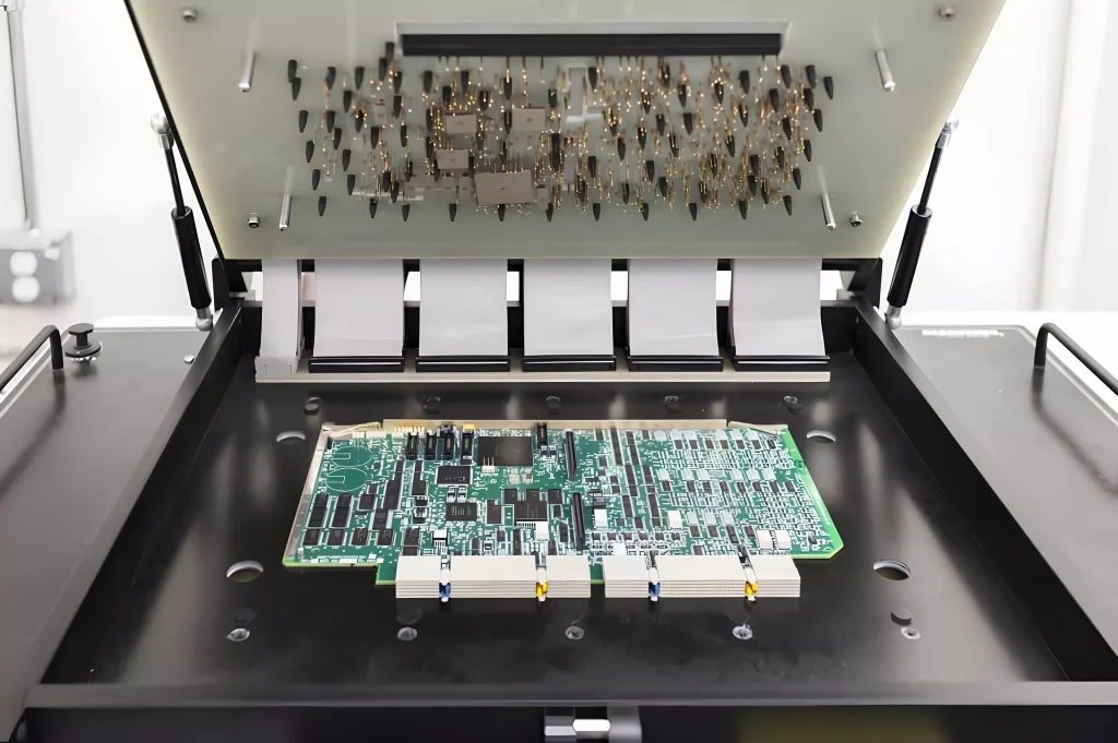
- In-Circuit Test (ICT): A “bed-of-nails” test fixture makes contact with hundreds of test points on the board. In seconds, it checks for shorts, opens, and verifies that each component has the correct value. It’s a fast, thorough check of the board’s basic health.
- Functional Circuit Test (FCT): This is the final exam. The board is powered up and tested under real operating conditions. For example, a motor drive board would be connected to a motor and put through start/stop cycles. This requires custom test fixtures and software but validates the board’s end-to-end performance.
4. Stress Testing for Long-Term Reliability
To ensure the board will last for years in the field, manufacturers simulate years of wear in a short time.
- Temperature Cycling: Boards are repeatedly cycled between hot and cold extremes (e.g., -10°C to +60°C for 50-500 cycles) to stress solder joints and materials.
- Operating Life & HALT Testing: Boards are baked at high temperatures (e.g., 85°C for 500-2000 hours) while running. Highly Accelerated Life Testing (HALT) combines extreme temperature swings with vibration to force any hidden weaknesses to fail before the board reaches the customer.


Industrial Control PCB Assembly Process Step by Step
1. Project Initiation & Design for Manufacturing (DFM) Analysis
A successful industrial PCBA project begins with a comprehensive exchange of technical documentation—including schematics, Gerber files, a detailed bill of materials (BOM) with approved manufacturer part numbers, centroid data, and test specifications. Before quoting, a thorough Design for Manufacturability (DFM) review is conducted to identify and mitigate risks related to fabrication, assembly, and long-term reliability.
The DFM process examines:
- Physical layout constraints, such as insufficient clearance between components and the solder paste stencil aperture, can affect paste release for fine-pitch devices.
- Documentation integrity, including misaligned reference designators or centroid files that could cause pick-and-place errors, and Gerber layer misassignment that may lead to fabrication defects.
- Pad geometry compliance with IPC standards to ensure proper solder joint formation and avoid bridges or insufficient fill.
Expert DFM feedback may include recommendations for trace width adjustment to meet fabrication capabilities, component repositioning to improve paste deposition, or alternate part suggestions to improve availability and cost. For legacy systems, reverse engineering services can generate accurate manufacturing documentation from existing hardware.
2. PCB Fabrication with Industrial-Grade Specifications
Although assembly is the core service, substrate quality dictates performance. Industrial PCBs often exceed consumer-grade specifications in several keys areas:
- Layer Stackup & Count: Designs commonly range from 4 to 16 layers, with high-complexity boards extending to 20+ layers. Stackups are engineered to provide dedicated ground planes for EMI control, power planes for low-impedance distribution, and signal layers with controlled impedance for high-speed communication.
- Material Selection: While FR-4 is widely used for its balance of cost and reliability, applications with high thermal loads—such as VFD controls dissipating 200+ watts—utilize high-Tg (glass transition temperature) materials like polyimide or enhanced epoxy for improved stability under thermal cycling.
- Copper Weight: Standard 1-ounce (35 µm) copper is sufficient for signal layers. 2-ounce (70 µm) copper is routinely specified for power distribution to increase current capacity. For very high-current applications (e.g., welding or battery charging systems), heavy copper (4-10 ounce) processes are employed to carry hundreds of amperes.
- Surface Finish & Solder Mask: Liquid Photoimageable (LPI) solder mask ensures precise feature definition. Surface finishes such as Immersion Silver, ENIG, or Lead-Free HASL are selected based on compatibility with RoHS-compliant lead-free assembly processes and required shelf life.
3. Component Sourcing, Verification & BOM Management
Reliable sourcing is critical, especially for extended-lifecycle products. Practices include:
- Procurement through authorized distributors and direct manufacturer channels to avoid counterfeit parts.
- Early BOM analysis to flag components with limited availability or approaching end-of-life.
- Maintenance of a strategic buffer inventory for long-lead-time industrial-grade components.
Incoming Quality Control (IQC) involves verifying component markings, electrical parameters, and physical condition. Full traceability documentation—including certificates of compliance and lot codes—is maintained for audit and failure analysis purposes.
4. SMT, THT & Mixed-Technology Assembly Processes
Industrial boards often integrate both Surface Mount Technology (SMT) and Through-Hole Technology (THT) components.
- SMT Assembly: High-precision chip shooters and placers handle components ranging from 01005 passives to fine-pitch BGA packages (0.4-0.5 mm pitch) with placement accuracy within ±100 µm. Solder paste is deposited using laser-cut or electroformed stencils, with volume carefully controlled to prevent bridging or insufficient solder.
- THT & Mixed Assembly: High-power devices, connectors, and transformers are often in through-hole packages. Automated insertion is used for high-volume standard parts, while manual insertion is employed for large or odd-form components.
- Soldering: SMT components are soldered in a controlled reflow oven with a thermally profiled ramp-soak-spike cycle. Wave soldering remains standard for THT parts, with modern systems using nitrogen inerting to reduce dross and improve wetting. For thermally sensitive assemblies, selective soldering provides localized, profile-controlled soldering of through-hole terminations.
5. Inspection, Testing, Programming & Systems Integration
A multi-tiered validation approach is employed:
- Automated Optical Inspection (AOI): Post-reflow, AOI systems compare board images to golden samples to detect defects such as tombstoning, bridging, or missing components, achieving 80-90% detection rates for common defects.
- X-Ray Inspection: Essential for hidden joints, such as those under BGA or QFN components, to identify voids, misalignment, or insufficient solder.
- In-Circuit Test (ICT): A bed-of-nails fixture verifies electrical connectivity, component value, and basic functionality at hundreds of test nodes within seconds.
- Functional Testing (FCT): The assembly is validated under simulated or real operational conditions—e.g., a motor drive board controlling a load—to ensure performance to specification.
- Programming & Configuration: Microcontrollers, FPGAs, and memory devices are programmed with customer firmware, often including secure boot loading and encryption.
- Box-Build / System Integration: The PCBA is installed into its enclosure, connected to wiring harnesses, and undergoes final system-level testing, delivering a turnkey solution.
6. Pilot Run & Ramp to Mass Production
A pilot run (typically 10-100 units) validates the entire manufacturing process before full-scale commitment. This phase:
- Confirms process stability, solder profile efficacy, and test coverage.
- Reveals design flaws or component issues that are less costly to correct at low volume.
- Establishes a baseline production yield. While a pilot yield of 85% may be acceptable for process debugging, mass production for industrial markets requires sustained yields above 95%.
- Informs final adjustments in tooling, operator training, and test software before high-volume release.
Common Challenges in Industrial Control PCBA Projects and How to Avoid Them
High Power and Thermal Management Issues
Industrial control applications handling 100+ watts of power dissipation present thermal challenges that dramatically impact reliability and lifespan. Poor thermal design results in component junction temperatures exceeding specification limits, accelerating semiconductor degradation and solder joint fatigue. Power semiconductor devices, including MOSFETs and diodes, commonly exhibit an inverse relationship between operating temperature and long-term reliability—a 10°C reduction in junction temperature can double device lifespan.
Effective thermal management begins with PCB design, addressing multiple mechanisms for heat dissipation. Power semiconductor mounting positions directly affect local PCB temperature. Mounting power devices near board edges or areas benefiting from airflow promotes heat dissipation. Mounting densities preventing adequate ventilation around heat-sink devices create thermal hotspots. Thermal simulation software during the design phase predicts temperature distribution and identifies thermal bottlenecks before manufacturing commitment.
Solder joint thermal management deserves specific attention. Power device solder joints experience cyclic temperature stress as semiconductor junctions heat and cool with device switching cycles. Insufficient solder volume under power packages creates high-stress solder joints prone to fatigue cracking after thousands of thermal cycles. Manufacturing process optimization ensures adequate solder paste under power device pads and validates through X-ray inspection that complete solder coverage exists before electrical testing.
Heat sink thermal resistance compounds junction temperature effects. A power MOSFET with 1°C/watt junction-to-case thermal resistance requires heat sink with case-to-ambient thermal resistance of 0.5°C/watt or lower to maintain acceptable operating temperatures at full power dissipation. PCBA manufacturing must ensure adequate thermal interface material—typically phase change pads or thermal grease—between the device case and the heat sink. Inadequate thermal interface material application increases thermal resistance and defeats heat sink performance.
Long-Term Reliability in Harsh Environments
Industrial environments subject control systems to temperature cycling, moisture, vibration, and electrical stress that do not significantly impact consumer products. Solder joint reliability under thermal cycling, moisture-induced corrosion, and mechanical fatigue represents primary concerns for long-lifecycle applications.
Temperature cycling stress results from thermal gradients between different PCB regions—power dissipation creates hotspots experiencing higher peak temperatures than surrounding areas, while overnight facility shutdown creates global temperature variations. Solder joints experience mechanical strain during thermal cycling as the PCB substrate and component bodies expand and contract at different rates. Thermal cycling testing as described above, predicts expected reliability and validates manufacturing process adequacy.
Moisture ingress accelerates corrosion of copper traces, solder joints, and component leads. Industrial facilities with humidity approaching 100% and temperature fluctuations create condensation cycles promoting moisture absorption into the epoxy PCB substrate. Conformal coating provides a protective layer preventing direct moisture contact with conductors and solder joints. Alternatively, potting—fully encapsulating the PCBA in epoxy compound—provides superior moisture protection but complicates field repair and reduces thermal dissipation capability.
Mechanical vibration in industrial environments including manufacturing equipment, vehicles, and mobile platforms stresses solder joints and component lead connections. Vibration testing quantifies anticipated operational stress and validates manufacturing process robustness. Large components including transformers and heat-sinked devices with poor mechanical support create high-stress solder joints prone to vibration-induced fatigue failure.
Electrical overstress and transient protection challenge industrial control designs operating in facilities with utility power disturbances and high-power switching equipment. Transient voltage suppressors and varistor devices protect sensitive inputs from electrical transients, while isolated power supplies prevent ground loop currents from damaging sensitive circuits. PCBA manufacturing must ensure proper grounding and decoupling capacitor placement to minimize transient voltage amplification.
Obsolescence and Component Shortages
Industrial control products designed for 10-15 year lifespans inevitably encounter component obsolescence as semiconductor manufacturers discontinue product lines. Design teams must establish obsolescence management strategies during the initial design phase rather than discovering supply challenges after the mass production ramp.
Proactive design practices specify devices with extended availability or identify qualified second sources during the design phase. Component manufacturers publish end-of-life (EOL) notifications years in advance of production termination, providing an opportunity for design modification or component inventory accumulation. Design teams should evaluate component manufacturer roadmaps and recommend design changes addressing known obsolescence risks before production commitment.
PCBA manufacturers support obsolescence management through BOM revision control and inventory programs. Qualified alternative component databases identify replacement devices meeting electrical and mechanical specifications. Bulk component purchasing and storage programs maintain an inventory of long-lead-time items, ensuring supply availability when primary sources deplete. For extended-lifecycle applications, IWDF Solutions and similar manufacturers maintain commitments to sustained production capability—including reserved inventory allocations and documented engineering change procedures ensuring product continuity throughout the contractual support period.

How to Choose an Industrial Control PCB Assembly Partner?
Selecting an appropriate PCBA manufacturing partner represents a strategic decision substantially impacting product development timelines, manufacturing cost, and field reliability. Technical capability and industry experience differentiate leading manufacturers from commodity assembly providers lacking specialized industrial control expertise.
| Selection Criterion | Generic PCBA House | Industrial Control-Focused Partner (IWDF Solutions) |
|---|---|---|
| Industry Experience | Comprehensive DFM analysis, thermal simulation, cost optimization, long-term lifecycle planning, and obsolescence management | 20+ years specializing in industrial automation, power electronics, automotive, and telecommunications |
| Certifications & Standards | Basic ISO 9001, limited advanced capability | ISO 9001, IPC-A-610 Class experience, RoHS/REACH compliance, IATF 16949 readiness, thermal profiling expertise |
| Service Scope | Assembly from customer-supplied BOM and Gerber | Integrated design, reverse engineering, PCB fabrication, component sourcing, assembly, testing, programming, box-build |
| Design & Engineering Support | Basic DFM checks, limited optimization | Proven expertise in high-power circuits, motor control, industrial communication protocols, and harsh-environment design |
| Industrial Application Knowledge | General manufacturing capability | AOI, X-ray, ICT, functional testing, stress screening, and environmental chamber validation |
| Quality Control Processes | Standard inspection (visual AOI) | Sustained production commitment, component inventory programs, documentation, archival, supply chain continuity |
| Long-Term Support | Limited commitment to extended production | Sustained production commitment, component inventory programs, documentation archival, supply chain continuity |
Manufacturers specializing in industrial control applications demonstrate commitment to extended customer support beyond initial production runs. Long-term partnership enables consistent quality, priority access to specialized components, and collaborative problem-solving when field issues emerge.
Why Global OEMs Choose IWDF Solutions for Industrial Control PCB Assembly
One-Stop Service from Design to Mass Production
IWDF Solutions provides integrated service delivery spanning the complete industrial control PCBA lifecycle. Customers presenting conceptual designs or prototype requirements receive design review, component recommendations, and manufacturing optimization recommendations before fabrication commitment. Established design-for-manufacturing (DFM) processes identify potential issues and optimize designs for manufacturing cost and reliability before production initiation.
PCB fabrication capability—with equipment supporting multi-layer boards, heavy copper processes, and controlled impedance requirements—eliminates dependency on external PCB suppliers and accelerates lead times. Integrated sourcing teams maintain relationships with global component distributors and direct suppliers, securing component allocations and managing supply chain continuity. Customers gain single-point accountability for design, fabrication, assembly, and test processes—reducing coordination overhead and enabling rapid issue resolution when challenges emerge.
One-stop service integration reduces customer operational burden particularly valuable for international customers. Rather than managing multiple supplier relationships across design consultants, PCB fabricators, component distributors, and assembly providers, IWDF Solutions coordinates all functions and delivers finished products ready for field deployment. Centralized quality control and documentation archival simplify compliance verification and facilitate future production ramps or product lifecycle support.
Industrial Control Project Experience and Engineering Team
IWDF Solutions maintains deep expertise across industrial control application domains accumulated through 20+ years of manufacturing experience. Engineering teams comprise 50+ professionals including hardware design engineers, manufacturing engineers, and quality specialists. This organizational depth enables technical problem-solving for complex industrial challenges and proactive identification of design improvements enhancing reliability or reducing cost.
Project portfolio spans 100+ countries and diverse industrial sectors including automation equipment, motor drives, renewable energy converters, industrial power supplies, and telecommunications infrastructure. Exposure to global industrial practices and regulatory requirements enables rapid assessment of customer applications and identification of potential manufacturing or compliance challenges. Established relationships with international logistics partners facilitate global shipping and supply chain management.
Quality, Traceability and On-Time Delivery
Industrial control applications demand consistent quality and reliable delivery schedules. IWDF Solutions implements comprehensive quality management systems addressing each stage of manufacturing: Incoming Quality Control (IQC) validates component specification and integrity before integration into assemblies; In-Process Quality Control (IPQC) monitors production processes ensuring adherence to established parameters; Final Quality Control (FQC) executes comprehensive testing before shipment. 100% Automated Optical Inspection (AOI) coverage, X-ray analysis for complex packages, and functional testing provide multi-layer quality assurance.
Material traceability programs document component sources, batch codes, and manufacturing dates—enabling rapid identification and resolution of component-related defects. Serialization of finished products and associated test data supports field diagnostics and root cause analysis when issues emerge after customer deployment.
On-time delivery performance reflects manufacturing excellence and supply chain management capability. IWDF Solutions targets 99.5% on-time delivery rates through capacity planning, supply chain buffering, and adaptive production scheduling. Customers gain confidence in receiving completed products within committed timeframes—critical for supply chain planning and customer commitments.
Case Study: Industrial Control PCBA Project from Prototype to Mass Production
A European industrial equipment manufacturer required a control module redesign for their motor speed regulation system. The legacy product utilized discrete analog circuitry with limited functionality and reliability issues in high-vibration applications. The customer sought to upgrade the control module, incorporating a modern microprocessor, advanced sensor interfaces, and industrial Ethernet communication capability while maintaining thermal performance within existing mechanical enclosures.
Project Challenges:
The redesigned control board integrated analog power management circuits, a microprocessor core with an LQFP package, motor current sensing with galvanic isolation, and CAN bus communication interface within a compact 150mm × 100mm footprint. The application environment included operating temperatures from -20°C to +70°C and motor starting transients generating electrical stress exceeding normal operating conditions. Existing customers required sustained product availability with no extended lead times for supply chain changes.
IWDF Solutions Approach:
Initial design review identified EMI susceptibility issues inherent in analog sensor circuitry and motor control switching. IWDF recommended digital signal conditioning for sensor interfaces and reinforced power supply filtering to mitigate noise coupling. Thermal simulation revealed inadequate heat sinking for the power semiconductor devices; IWDF engineers modified the substrate layout incorporating plated-through vias beneath power devices improving thermal conductance to the secondary heat sink surface. PCB substrate thickness increased from standard 1.6mm to 2.4mm accommodating heavy copper requirements for motor current switching traces.
Component selection incorporated second-source strategies addressing obsolescence risk for specialized motor control integrated circuits. Strategic inventory accumulation secured component allocations protecting against future supply disruptions.
Pilot Production Results:
Initial pilot production of 50 units achieved 92% first-pass yield. X-ray analysis revealed marginal solder coverage on selected BGA balls—reflow temperature profile adjustment increased peak temperature by 8°C ensuring complete wetting without exceeding component thermal limits. Functional testing executing motor speed regulation algorithms under simulated load conditions validated control performance and protective shutdown behaviors.
Production Ramp:
Subsequent production ramp achieved 98.5% yield with consistent quality metrics. 12-month production sustained 5,000 units monthly volume—well exceeding the customer’s 2,000 unit requirements. IWDF’s supply chain management prevented component supply disruptions despite semiconductor industry-wide shortages of motor control devices. End-to-end product delivery from design initiation to mass production achieved a 6-month schedule—meeting the customer’s competitive product launch timeline.
The customer reported 40% reduction in field failures compared to legacy analog control boards and commended IWDF’s collaborative approach to thermal management challenges and obsolescence planning.
How to Start Your Industrial Control PCB Assembly Project with IWDF Solutions?
What Files Do You Need to Prepare?
Successful PCBA projects begin with comprehensive technical documentation providing manufacturing teams with a complete context for cost estimation and production planning. Standard deliverables include:
Schematic Diagram: Complete circuit schematic in industry-standard electronic design automation (EDA) format (OrCAD, Altium, KiCAD) or PDF representation detailing all electrical connections, component values, and functional blocks. Schematics should clearly identify signal names and voltage references supporting the layout engineer’s verification of interconnect accuracy.
PCB Layout Gerber Files: Manufacturing-ready files defining copper trace layers, solder mask openings, silkscreen component identifiers, and drill coordinates in Gerber 274X format. Gerber files should include layer stackup definition and any mechanical features such as edge connectors or mounting hole locations.
Bill of Materials (BOM): Comprehensive component listing including reference designators, manufacturer part numbers, component descriptions, quantities per board, and supplier recommendations. Preferred format includes component datasheets or specifications enabling PCBA engineering teams to verify compatibility with manufacturing processes.
Assembly Coordinate File: Precise placement data (.xy or .csv format) specifying X and Y coordinates, rotation angle, and reference designator for each component requiring placement. Pick-and-place machine programming depends on accurate coordinate data—deviations of 0.1mm or greater can misalign fine-pitch components and compromise solder joint quality.
Test Specifications: Functional requirements and acceptance criteria defining behaviors expected from completed assemblies. Functional test specifications support custom test program development and enable validation that manufacturing processes achieve design intent.
Existing Product Samples (for reverse engineering): For applications where current documentation is incomplete or unavailable, IWDF Solutions accepts physical products for PCB reverse engineering. Engineering teams remove image components, trace copper paths on each layer, and reconstruct complete manufacturing documentation suitable for production ramp.
Simple Engagement Process
IWDF Solutions streamlines customer engagement through a five-step collaborative process:
Step 1 – Technical Submission & Initial Assessment (48-72 hours): Customer submits technical documentation, design files, and project requirements through web portal or email. IWDF technical team conducts an initial completeness review and identifies any missing information. Preliminary assessment identifies potential manufacturability challenges or component supply considerations requiring customer awareness.
Step 2 – Design-for-Manufacturability Analysis & Cost Estimation (3-5 business days): Comprehensive DFM analysis identifies design optimizations enhancing manufacturability or reducing cost without compromising functionality. Engineering recommendations address specific concerns identified during initial assessment. Detailed quotation includes material costs, labor, testing, and overhead allocations, enabling customer cost planning. Lead time estimates reflect current component availability and production capacity.
Step 3 – Design Refinement & Tooling Preparation (2-4 weeks): Customer reviews recommendations and approves quotation. IWDF technical teams finalize PCB artwork, including solder paste stencil design, component placement optimization, and test fixture design if custom testing is required. PCB fabrication orders are submitted, initiating manufacturing of test boards and production substrates.
Step 4 – Pilot Production & Validation (2-4 weeks): Initial pilot build of 10-50 units exercises all manufacturing processes and test procedures. Design validation testing ensures electrical functionality meets requirements. Minor design modifications or process adjustments identified during pilot production are implemented before mass production commitment.
Step 5 – Mass Production & Ongoing Support (4+ weeks): Production ramps to customer-specified monthly volume. Regular production reports document yield metrics, test results, and ongoing quality assurance activities. IWDF maintains product documentation and component traceability records supporting future production batches or field service requirements.
Final
Companies seeking a reliable industrial control PCB assembly partner enabling design innovation and manufacturing scale should initiate engagement with IWDF Solutions. Our integrated service model—spanning design consultation, component sourcing, precision manufacturing, comprehensive testing, and long-term supply commitment—provides risk mitigation and operational efficiency beyond traditional assembly providers.
Contact IWDF Solutions to schedule a technical consultation and receive a comprehensive quotation for your industrial control PCBA project.
Our technical team commits to providing an initial quotation and engineering assessment within 48 hours of documentation submission. Whether evaluating manufacturing viability for prototype designs or scaling production from thousands to tens of thousands of units monthly, IWDF Solutions provides the expertise, infrastructure, and collaborative approach driving project success and sustained field reliability.

