

Your high-speed board keeps failing SI or EMC tests. You trace the layout for hours and find no obvious error. The real problem is usually somewhere you did not look: uncontrolled trace impedance.
Impedance control in PCB design means building key traces so their characteristic impedance matches a required value — typically 50 Ω, 90 Ω, or 100 Ω — within a defined tolerance. For any board with USB, HDMI, DDR, PCIe, Ethernet, or RF signals, it directly determines whether the product works and passes compliance testing.
This guide is not about theory. It is about decisions. By the end, you will know when impedance control applies to your board, which values to use for each interface, which structure and material to choose, and exactly how to write a specification that your PCB manufacturer can build and verify.
What Is Impedance Control in PCB Design?
Impedance control in PCB design means that specific traces — together with their reference planes — form a transmission line with a defined characteristic impedance, in ohms (Ω). The goal is to keep that impedance matched to the interface requirement along the full signal path, so the signal travels without reflection or distortion.
Characteristic impedance is determined by three physical things: trace geometry (width and copper thickness), the distance from the trace to its reference plane, and the dielectric constant (Dk) of the PCB material between them. Change any one of these, and impedance changes.

For high-speed interfaces like USB, HDMI, PCIe, DDR, Ethernet, and RF above 100 MHz, a trace can no longer be treated as a simple wire. It behaves as a transmission line. The signal travels as a wave, and if it meets an impedance change at any point along the path, part of the energy reflects back. Those reflections collapse the eye diagram, cause bit errors, and increase EMI radiation.
When Does Impedance Control Start to Apply?
The practical trigger is this: when the trace length becomes significant compared to the signal’s rise time, transmission line effects begin. A commonly used rule is that if your trace exceeds one-third of the distance the signal travels during its rise time, treat it as a transmission line and control its impedance.
For modern interfaces with rise times in the nanosecond or sub-nanosecond range, this threshold is reached quickly — often at just a few centimeters. That is why impedance control is now standard practice on most high-speed digital boards, not just RF designs.
Which PCB Transmission Lines Need Impedance Control?
In real boards, the following line types most commonly require controlled impedance:
| Line Type | Description |
|---|---|
| Single-ended microstrip | Outer-layer trace over a single reference plane |
| Single-ended stripline | Inner-layer trace between two reference planes |
| Differential microstrip pair | Two outer-layer traces routed as a coupled pair |
| Differential stripline pair | Two inner-layer traces routed as a coupled pair |
| Embedded microstrip | Outer-like trace partially buried in laminate |
| Coplanar (single or differential) | Trace with ground copper on the same layer as side guards |
The rest of this guide covers every decision you need to make for these line types — from choosing a structure and material to writing a specification that a factory can build and test against.
When Does Your PCB Actually Need Impedance Control?
Not every board needs impedance control. Applying it where it is not needed adds cost. Missing it where it is needed causes failures. Here is how to make the right call quickly.
A PCB needs impedance control when it carries signals fast enough to behave as transmission lines. In practice, check the interface type, data rate, and trace length. If the board handles USB, HDMI, PCIe, DDR, Ethernet, or any RF path, those nets need controlled impedance.
Interface-Based Decision Table
| Signal / Interface | Typical Data Rate | Impedance Control? |
|---|---|---|
| GPIO, LEDs, slow buttons | < 10 MHz | No |
| Low-speed UART / SPI | < 10 MHz, short traces | No |
| SPI long runs / off-board | 10–50 MHz, > 50 mm | Yes |
| USB 2.0 High Speed | 480 Mbps | Yes |
| USB 3.x / USB4 | 5–80 Gbps | Yes |
| HDMI / DisplayPort | 3–48 Gbps | Yes |
| MIPI DSI / CSI | 1–4 Gbps per lane | Yes |
| DDR2 / DDR3 / DDR4 / DDR5 | Up to 6.4 GT/s | Yes |
| Ethernet 100M / 1G / 10G | All | Yes |
| PCIe Gen2 and above | 5 GT/s and above | Yes |
| RF paths | > 100 MHz | Yes |
If your board has at least one “Yes” row, design and order it as an impedance control PCB.
What Happens If You Skip It?
The consequences are concrete, not theoretical:
- Differential pairs lose noise rejection, causing intermittent link training failures
- Eye diagrams collapse, especially at temperature extremes or across board batches
- EMC pre-compliance fails at frequencies that trace lengths happen to resonate
- High-speed memory passes on some boards but fails on others from the same production run
- Re-spins cost three to five times more than the impedance control you skipped
What Impedance Value Should You Target for Each Interface?
Once you know your board needs controlled impedance, the next question is: which specific numbers do you put in the specification? Getting these wrong will fail compliance testing even if the fabrication is perfect.
Target impedance values come from interface standards — USB-IF, HDMI Forum, PCI-SIG, JEDEC, IEEE. The most common values are 50 Ω for single-ended RF and clock traces, 90 Ω for USB differential pairs, and 100 Ω for Ethernet, HDMI, and SATA. These numbers go directly into your fabrication drawing as the verified specification.
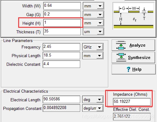
Standard Interface Impedance Reference
| Interface | Signal Type | Target Impedance | Tolerance |
|---|---|---|---|
| Single-ended RF / clock | Single-ended | 50 Ω | ±10% |
| USB 2.0 High Speed | Differential | 90 Ω | ±10% |
| USB 3.x | Differential | 90 Ω | ±10% |
| USB4 | Differential | 85 Ω | ±10% |
| HDMI 1.4 | Differential | 100 Ω | ±15% |
| HDMI 2.0 / 2.1 | Differential | 100 Ω | ±10% |
| Ethernet 100M / 1G | Differential | 100 Ω | ±10% |
| PCIe Gen3 | Differential | 85 Ω | ±15% |
| PCIe Gen4 / Gen5 | Differential | 85 Ω | ±10% |
| DDR4 data lines | Single-ended | 40–50 Ω | ±10% |
| SATA III | Differential | 100 Ω | ±10% |
Why 50 Ω, 90 Ω, and 100 Ω Dominate?
- 50 Ω is the compromise between minimum signal loss and maximum power handling for coaxial and single-ended transmission lines. It became the universal RF and single-ended high-speed standard because it balances both.
- 90 Ω was defined for USB differential pairs to minimize crosstalk in tight consumer electronics layouts while keeping signal levels within the USB specification.
- 100 Ω suits Ethernet and HDMI because differential signaling at higher impedance reduces driver output current demands and improves noise immunity across longer traces and cables.
For any high-speed signal that does not belong to a defined standard — for example, a local clock line — 50 Ω is the safest default.
What Factors Actually Control Trace Impedance?
Knowing the target value is not enough. You also need to understand what physical parameters produce that value on a real board, so you can review a manufacturer’s stack-up proposal and catch problems before production.
Seven physical parameters determine characteristic impedance: trace width, dielectric constant (Dk), dielectric thickness, copper thickness, stack-up arrangement, differential pair spacing, and solder mask. Every impedance calculator and field solver uses these same inputs. Understanding what each one does helps you communicate clearly with your manufacturer and avoid mismatches between simulation and real boards.
The Seven Factors and Their Effects
| Factor | Change | Effect on Impedance |
|---|---|---|
| Trace width | Wider | Lower |
| Dielectric constant (Dk) | Higher | Lower |
| Dielectric thickness (trace to plane) | Thicker | Higher |
| Copper thickness | Thicker | Lower |
| Differential pair spacing | Closer | Lower (differential Z) |
| Solder mask over trace | Present | Slightly lower |
| Temperature / humidity | Higher | Small decrease |
Three things are especially worth knowing in practice:
- A width change of just 0.025 mm can shift impedance by 5–6 Ω on a typical FR-4 stack-up. This is why your specification must include calculated widths, not default values from an EDA template.
- Standard FR-4 has a Dk of about 3.9–4.5 at low frequencies, but this drops to around 3.4–3.7 at 5 GHz. That shift quietly pulls impedance away from the target at high frequencies if the manufacturer uses a generic Dk number instead of real material data.
- Solder mask on outer-layer traces adds a thin extra dielectric layer. Most impedance calculators let you choose “with mask” or “without mask” — make sure the choice matches your actual board finish.
These seven factors are what every impedance calculation is built on. Two of them drive the most important early design choices: the transmission line structure and the substrate material. These are decisions you must make before routing begins, and before you can write a valid specification.
Microstrip or Stripline: How Should You Choose Your Transmission Line Structure?
Before you route a single high-speed trace, you need to answer one question: should these signals go on outer layers or inner layers? That choice sets your stack-up, your EMI behavior, and much of your cost.
Microstrip routes on outer layers above a single reference plane. Stripline routes on inner layers between two reference planes. Microstrip is wider, easier to manufacture, and easier to probe. Stripline offers better shielding and is preferred for very high speeds or noise-sensitive routes. Most real boards use both structures in different areas.
Microstrip vs Stripline Comparison
| Property | Microstrip | Stripline |
|---|---|---|
| Layer position | Outer (top / bottom) | Inner (buried) |
| Reference planes | One below | One above, one below |
| EMI shielding | Open on one side — more radiation | Fully enclosed — better shielding |
| Trace width for 50 Ω | Wider — easier to manufacture | Narrower — tighter process tolerance |
| Signal propagation speed | Faster (air lowers effective Dk) | Slower (full substrate Dk) |
| Post-fabrication accessibility | Easy to probe and rework | Not accessible after lamination |
| Typical use | USB / HDMI / Ethernet connectors, DDR bus | High-speed SerDes backbone, RF inner layer |

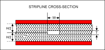
Practical Decision Rules
Use microstrip when interfaces are USB, HDMI, Ethernet, PCIe, or DDR and frequencies stay below about 5 GHz. It is lower cost and easier to probe during bring-up.
Use stripline when you need strong EMI shielding, when frequencies exceed 5 GHz, or when you are routing high-speed backbone traces across a large board where reference plane continuity is critical.
Use coplanar waveguide (CPW) for RF sections where the distance to the plane below is hard to control, for flex PCBs where stack-up depth varies, or when you need additional lateral shielding on an outer-layer RF path.
Once you have assigned signal groups to layers and chosen a structure for each, the stack-up framework is set. The next decision — which material to use — determines whether you can actually hold your impedance targets with that structure in volume production.
FR-4 or Rogers: What Substrate Material Should You Specify?
Many engineers default to FR-4 because it is familiar and cost-effective. That is the right call for many designs. At higher frequencies or with tighter tolerances, however, the wrong material makes reliable impedance control impossible.
The substrate material controls the dielectric constant (Dk) in every impedance calculation. Standard FR-4 works well for most designs below 3 GHz at ±10% tolerance. Above 3 GHz, or when ±5% or better is required, Rogers or similar low-loss materials provide more stable Dk and lower insertion loss across the frequency range.
Material Comparison Table
| Property | FR-4 Standard | FR-4 High-Tg | Rogers RO4003C | Rogers RO4350B | PTFE-based |
|---|---|---|---|---|---|
| Dk (typical) | 3.9–4.5 | 3.9–4.5 | ~3.38 | ~3.48 | 2.2–3.0 |
| Dk stability vs frequency | Poor above 3 GHz | Moderate | Excellent | Excellent | Excellent |
| Loss tangent (Df) | 0.020–0.025 | 0.018–0.022 | 0.0027 | 0.0037 | 0.0009–0.002 |
| Achievable impedance tolerance | ±10% | ±10% | ±5% | ±5% | ±5% |
| Cost | $ | $$ | $$$ | $$$ | $$$$ |
| Process compatibility | Standard | Standard | FR-4 compatible | FR-4 compatible | Specialized |
Three Selection Rules
- Highest frequency below 3 GHz and ±10% tolerance acceptable — use FR-4 or high-Tg FR-4.
- Frequency 3–10 GHz or ±5% tolerance required — use Rogers RO4003C or RO4350B. Both process on standard FR-4 equipment, so no special production line is needed.
- Frequency above 10 GHz or very low insertion loss needed — use PTFE-based materials. Cost and lead time will increase significantly.
The Hybrid Stack-Up Option
When a design combines RF sections with standard digital layers, a hybrid stack-up is often the best answer. Use Rogers or a high-frequency laminate on the outer layers for RF paths and antennas. Use standard FR-4 for inner power and lower-speed digital layers. This approach keeps cost in check while meeting performance where it actually matters.
With structure and material decided, you now have everything you need to translate your design decisions into a specification your manufacturer can execute without guesswork.
How to Specify Impedance Control Requirements Correctly to Your Manufacturer?
Most impedance failures do not happen during routing. They happen at the handoff to the factory. Vague or incomplete documentation forces the manufacturer to make assumptions — and assumptions produce boards that do not match your design.
A correct impedance specification includes four things: a stack-up table with layer materials and copper weights, an impedance table mapping target values and tolerances to specific layers, a transmission line type for each impedance class, and explicit testing requirements. Together, these give the manufacturer no room for guesswork.
Step 1: Define Your Stack-Up
Include a layer table in your fabrication drawing:
| Layer | Name | Type | Copper Weight | Dielectric to Next Layer | Material |
|---|---|---|---|---|---|
| L1 | Top | Signal | 1 oz | 0.10 mm to L2 | Prepreg FR-4 |
| L2 | GND | Plane | 1 oz | 0.20 mm to L3 | Core FR-4 |
| L3 | Inner 1 | Signal | 0.5 oz | 0.20 mm to L4 | Core FR-4 |
| L4 | Inner 2 | Signal | 0.5 oz | 0.20 mm to L5 | Core FR-4 |
| L5 | GND | Plane | 1 oz | 0.10 mm to L6 | Prepreg FR-4 |
| L6 | Bottom | Signal | 1 oz | — | — |
Add a note: “Manufacturer may adjust stack-up dielectric thicknesses to meet impedance targets, subject to customer approval before production.”

Step 2: Build an Impedance Table
This table is the core of your specification. Every row is one impedance requirement:
| ID | Type | Target (Ω) | Tolerance | Trace Width (mm) | Spacing (mm) | Layers | Reference Planes | Application |
|---|---|---|---|---|---|---|---|---|
| Z1 | Single-ended | 50 | ±10% | 0.20 | — | L1 | L2 GND | RF / clock nets |
| Z2 | Differential | 90 | ±10% | 0.15 | 0.18 | L1 | L2 GND | USB 3.x pairs |
| Z3 | Differential | 100 | ±10% | 0.14 | 0.20 | L3 | L2+L4 GND | Ethernet / HDMI |
If you have run your own simulation, include the trace widths. If not, leave them blank and let the manufacturer calculate from your target impedance and stack-up. Either way, the Target, Tolerance, Layer, and Reference Plane columns must always be filled.
Step 3: Specify Testing Requirements in the Fab Notes
Include these three lines in your fabrication notes:
- “Controlled impedance required for Z1, Z2, Z3 as per impedance table above.”
- “TDR test coupons required for each impedance class.”
- “Provide TDR report showing measured value, target value, tolerance, and pass/fail for each coupon. Report must accompany delivery.”
Without written testing requirements, many factories — especially on prototype quantities — will skip TDR testing entirely.
Step 4: Require Approval Before Any Stack-Up Change
Add one more note:
“If manufacturer proposes any change to stack-up, dielectric material, or trace widths to meet impedance targets, customer approval is required before production begins.”
This single line prevents the most common production surprise: boards that arrive built to a different stack-up than the one your routing was based on.
How Do Manufacturers Verify Impedance After Fabrication?
Writing a correct specification is necessary. But you also need to confirm that the manufacturer actually hit your targets. Here is what a proper verification looks like and what to check in the report.
Factories verify controlled impedance using TDR — Time Domain Reflectometry. They fabricate test coupons on the same production panel as your boards. These coupons copy your exact stack-up and trace geometry. A TDR instrument sends a fast pulse down the coupon trace and measures reflections to produce an impedance-vs-distance curve. The flat middle section of that curve is the valid reading zone.
What does a TDR Coupon contain?
A coupon is a small section on the production panel — typically about 200 mm × 30 mm. It contains straight trace segments for each impedance type you specified. It is built with the same copper weights, laminates, and prepregs as your real boards, processed in the same production run.
How to Read a TDR Report?
A complete TDR report should include:
- one measured value per coupon trace
- target impedance, tolerance range, measured value, and pass/fail status
- a waveform plot showing impedance along the trace length
- instrument model, calibration date, and test temperature
The valid reading zone in the waveform is the flat plateau in the middle of the trace. The first part of the curve reflects the probe contact, not the trace impedance — ignore it. The end of the curve reflects the termination — also ignore it.
If a coupon reading falls outside your tolerance, the correct action from the factory is to hold shipment, investigate the cause, and contact you before anything ships. Make this expectation explicit in your purchase order terms.
10 Practical Design Rules for Impedance Controlled PCBs
These rules are not general advice. Each one addresses a specific, repeatable failure mode that shows up in real production. Follow all ten and your impedance-controlled board has a much higher chance of passing TDR verification and signal integrity testing on the first build.
Rule 1: Make Controlled Impedance Traces Visually Different from Other Traces
If your controlled impedance traces use the same width as other non-critical traces on the same layer, your PCB manufacturer cannot tell them apart. The result is that the factory either controls impedance on the wrong traces, or asks you a string of engineering queries that delay production.
The fix is simple: use a width that is slightly different from any other trace on the same layer.
For example, if your standard signal traces are 5.0 mil, make your 50 Ω impedance traces 5.1 mil or 4.9 mil. The impedance difference is negligible. But the visual difference tells the factory exactly which traces are controlled.
A practical example of reserved widths for controlled impedance on a standard 6-layer FR-4 board:
| Layer | Structure | Type | Impedance Type | Target (Ω) | Reserved Trace Width | Spacing (diff) | Reference Plane |
|---|---|---|---|---|---|---|---|
| L1 | Microstrip | Signal | Single-ended | 50 | 5.1 mil | — | L2 GND |
| L1 | Microstrip | Signal | Differential | 90 | 4.1 mil | 5.6 mil | L2 GND |
| L1 | Microstrip | Signal | Differential | 100 | 3.6 mil | 6.1 mil | L2 GND |
| L2 | — | GND | — | — | — | — | — |
| L3 | Stripline | Signal | Single-ended | 50 | 4.3 mil | — | L2 + L4 GND |
| L3 | Stripline | Signal | Differential | 90 | 3.6 mil | 5.3 mil | L2 + L4 GND |
| L3 | Stripline | Signal | Differential | 100 | 3.1 mil | 5.8 mil | L2 + L4 GND |
| L4 | Stripline | Signal | Single-ended | 50 | 4.3 mil | — | L3 + L5 GND |
| L4 | Stripline | Signal | Differential | 90 | 3.6 mil | 5.3 mil | L3 + L5 GND |
| L4 | Stripline | Signal | Differential | 100 | 3.1 mil | 5.8 mil | L3 + L5 GND |
| L5 | — | GND | — | — | — | — | — |
| L6 | Microstrip | Signal | Single-ended | 50 | 5.1 mil | — | L5 GND |
| L6 | Microstrip | Signal | Differential | 90 | 4.1 mil | 5.6 mil | L5 GND |
| L6 | Microstrip | Signal | Differential | 100 | 3.6 mil | 6.1 mil | L5 GND |
Do not route any non-impedance signal with these reserved widths. This single discipline eliminates one of the most common communication failures between the designer and factory.
Rule 2: Agree on the Stack-Up with Your Factory Before You Route
Lock your stack-up with the manufacturer before you start detailed routing — not after.
Your EDA tool uses generic Dk values that do not necessarily match the real material your factory stocks. A 0.02 difference in Dk between your simulation and the real laminate can shift impedance by 4–6 Ω. If you route the entire board first and then discover the calculated widths do not match what is manufacturable, you face a full re-route.
The right sequence is: share your target impedances and layer count early, ask the factory to return a confirmed stack-up with real material data and confirmed trace widths, then route to those numbers. Never use your EDA tool’s default stack-up as the basis for final routing dimensions.
Rule 3: Keep a Continuous Reference Plane Under Every Controlled Impedance Trace
A controlled impedance trace is only controlled when it has a consistent, unbroken reference plane directly below or above it for the entire route length.
Slots, plane splits, dense via clusters, and power islands all break that reference plane. When the return current path is broken, three things happen simultaneously: local impedance shifts unpredictably, loop area increases and radiates EMI, and signal integrity degrades in ways that are very hard to debug because they do not appear as DRC violations.
Before routing, confirm that every high-speed signal layer has a solid, unbroken reference plane on the adjacent layer. If a plane split is unavoidable, place stitching capacitors of 10–100 nF directly across the split to give the return current a short, low-inductance crossing path.

Rule 4: Keep Differential Pair Geometry Constant From Pad to Pad
Differential impedance depends on two things: trace width and the spacing between the two traces. Both must stay constant for the full routed length — not just in the open areas between pads.
The most common failure point is around component pads and via fanouts, where spacing briefly widens. Each spacing change is a localized impedance discontinuity. Multiple small discontinuities accumulate and collapse the differential signal’s common-mode rejection at the receiver.
Route each pair with the same width and spacing from the driver pad to the receiver pad. Where a pad forces a geometry change, keep that section as short as possible and symmetrical on both traces. If a via is needed on one trace, place a matching via on the other trace at the same location.

Rule 5: Correct Intra-Pair Length Skew Close to the Source
In a differential pair, both traces must arrive at the receiver at the same time. A length mismatch converts part of the differential signal into common-mode noise and creates timing errors.
Each interface standard defines a maximum intra-pair skew:
| Interface | Max Intra-Pair Skew |
|---|---|
| USB 2.0 HS | 100 ps |
| USB 3.x | ~5 mil (< 1 ps practical) |
| PCIe Gen3 | 1.0 ps per inch recommended |
| HDMI 2.0 | 0.15 UI at the connector |
| DDR4 | ±1 ps within byte lane |
Where pin placement forces one trace to start longer, correct the mismatch by adding a small serpentine section to the shorter trace. Place the correction close to the source end of the pair, not spread along the full route. Keep the meander amplitude less than three times the trace width and the pitch tight — a loose, wide serpentine introduces its own impedance variation.

Rule 6: Treat Vias as Impedance Events, Not Just Connections
Most designers focus on trace geometry and overlook vias. A via is not electrically transparent. It introduces a local impedance discontinuity because its pad, anti-pad, and barrel geometry create a capacitive and inductive effect that is different from the trace on either side.
Two via-related problems appear most often on high-speed boards:
Via stubs. On a through-hole via, the unused portion below the exit layer acts as a resonant stub. At high data rates, this stub creates a notch in insertion loss. For PCIe Gen3 and above, SATA, 10G Ethernet, and USB 3.x, the stub resonance can fall inside the signal band and cause link failures.
Solutions in order of cost:
- Use blind or buried vias to eliminate the stub entirely
- Use back-drilling (controlled-depth drilling) to remove the stub after lamination
- If through-hole vias are unavoidable, minimize the stub length by choosing the shallowest exit layer possible
Missing return path vias. When a signal changes layers through a via, its return current must also find a path to the new reference plane. If there is no stitching via nearby, the return current takes a long detour through the plane, which increases loop area and creates an impedance bump at the transition.

Fix: always place at least two ground stitching vias within 0.5 mm of every signal via on a controlled impedance net.
Rule 7: Apply the 3W and 5W Rules to Prevent Crosstalk
Controlling your own trace impedance is not enough if a neighboring trace is electromagnetically coupled to it. Crosstalk introduces noise that changes the effective signal level seen by the receiver and cannot be fixed by impedance matching alone.
Two practical spacing rules apply:
3W rule for single-ended traces: the edge-to-edge spacing between two parallel single-ended traces should be at least three times the trace width. This keeps mutual coupling below approximately 10%.
5W rule for differential pairs: the edge-to-edge spacing between two separate differential pairs should be at least five times the trace width of a single trace. This prevents one pair from degrading the common-mode rejection of its neighbor.
In practice:
- Apply 3W spacing to all parallel single-ended impedance traces
- Apply 5W spacing between adjacent differential pairs
- Minimize the parallel run length between any two high-speed nets that cannot meet these rules
- Add a grounded guard trace between a high-speed signal and a sensitive analog line if spacing is unavoidable

Rule 8: Account for Solder Mask When Calculating Outer-Layer Impedance
Solder mask is a dielectric. When applied over an outer-layer trace, it adds a thin extra dielectric layer on top of the copper, which lowers impedance compared to a bare trace in air.
The shift is small but real: typically 2–5 Ω lower than a “no mask” calculation. On a 50 Ω target with ±10% tolerance, this shift eats 20–50% of your tolerance budget before you have measured anything.
Most field solvers and impedance calculators have a “with solder mask” option. Use it. Input the actual mask thickness (typically 0.01–0.03 mm) and its Dk (typically 3.3–4.0 depending on the mask product). The resulting trace width will be slightly different from a bare-trace calculation, and that difference is real.
If your outer-layer controlled impedance traces are in an area without solder mask coverage (for example, near a connector or under a component that requires a mask opening), calculate impedance separately for the masked and unmasked sections.

Rule 9: Use Your TDR Report as a Layout Debug Tool, Not Just an Acceptance Document
Most engineers treat the TDR report as a pass/fail certificate at delivery. It is actually more useful than that. The waveform plot in a TDR report shows you exactly where impedance changes along the trace — which means it can tell you where a layout or fabrication problem is physically located.
How to read it:
- A smooth, flat plateau in the middle of the waveform means the trace is well-controlled for that section
- A dip (lower impedance) in one zone means the trace is too wide, the dielectric is too thin, or solder mask is heavier in that area
- A peak (higher impedance) in one zone means the trace is too narrow, there is a plane void below it, or the dielectric is thicker in that region
- A sharp spike anywhere means a via, a pad, a plane split, or a geometry change is creating a discontinuity at that physical location
If your first prototype comes back with a TDR report that shows a peak in one specific region, that region corresponds to a real physical location on your board. You can calculate the approximate distance using the signal propagation speed for your material. Use that to identify whether the issue is a routing decision you can change or a fabrication variation the factory needs to address.
Rule 10: Validate Your Impedance Stack-Up Against Real Material Data, Not Just a Calculator Default
Every impedance calculator gives you a number. That number is only as accurate as the Dk and dielectric thickness values you put into it.
Standard FR-4 laminate has a nominal Dk of about 4.4 at 1 MHz, but the actual value depends on resin content, glass weave style, and measurement frequency. At 1 GHz, the same material may have a Dk closer to 4.0–4.2. At 5 GHz, it may be 3.8–4.0. If you calculate trace width using 4.4 at a frequency of 1 GHz, your trace will come out with higher impedance than expected because the real Dk is lower.
Practical steps:
- Ask your PCB manufacturer for the actual Dk vs. frequency curve for the specific material they plan to use, not just the datasheet nominal value
- If the material brand or grade changes between your prototype and production runs, ask the factory to reconfirm impedance calculations against the new material data
- For Rogers and other controlled-Dk materials, the datasheet Dk is much more reliable — but still confirm that the factory is using the same grade you specified, not a substitution
The goal is to ensure your EDA simulation and the factory’s field solver are using the same material numbers. When they match, the manufactured board matches your design intent.
Frequently Asked Questions About Impedance Control PCB
What is a standard impedance tolerance for PCB manufacturing?
For most commercial and industrial boards, ±10% is the standard. This corresponds to IPC Class 2, which covers the majority of consumer electronics, telecom, and industrial products. IPC Class 3 — used for medical, aerospace, and military applications — typically requires ±5%. For impedance values below 50 Ω, an absolute tolerance of ±5 Ω is often applied instead of a percentage.
Can a 2-layer PCB support impedance control?
Yes, but with real limitations. On a 2-layer board, you route the controlled impedance trace on the top layer and use the bottom layer as a solid ground reference. This works for basic single-ended microstrip. Differential pair control is harder because there is no buried layer for the return path. For any serious high-speed design, a 4-layer or higher stack-up gives you much better results and more routing flexibility.
How much does impedance control add to PCB cost?
Typically 5–15% above the base PCB price. This covers stack-up engineering, material selection, TDR coupon fabrication, testing, and the written report. In almost every case, this cost is lower than the cost of one unplanned re-spin caused by an impedance miss.
What files do I need to provide for an impedance control PCB quote?
You need Gerber or ODB++ files, a stack-up definition or your layer count and thickness constraints, an impedance table with target values and tolerances, identification of which layers carry controlled impedance traces, material preferences, and quantity with required lead time. The more complete your package, the faster the quote and the fewer engineering holds during production.
Can FR-4 be used for 5G designs?
For sub-6 GHz 5G paths, high-Tg FR-4 can work on less frequency-sensitive traces. For RF-critical paths at these frequencies, Rogers RO4003C or RO4350B is a safer choice. For 5G mmWave above 24 GHz, standard FR-4 is not suitable. Its Dk is too unstable at those frequencies. Rogers, Isola, or PTFE-based materials are the standard for mmWave work.
What is a TDR test coupon and do I always need one?
A TDR test coupon is a small trace section built on the same production panel as your boards. It replicates your exact impedance-controlled trace geometry and is used to measure whether your impedance target was actually achieved after fabrication. For any board where signal integrity matters — which means any board where you specified impedance control — always request TDR coupon testing and a written report. It is the only objective proof that your specification was met.
What is the difference between single-ended and differential impedance?
Single-ended impedance is measured from one trace to the ground plane reference. Differential impedance is measured between the two traces of a pair, with the ground planes as a shared reference. Single-ended 50 Ω applies to RF traces, clock lines, and individual high-speed signals. Differential 90 Ω or 100 Ω applies to interfaces that transmit data as complementary pairs — USB, HDMI, Ethernet, PCIe, and most modern high-speed serial buses.
How do I know if my manufacturer actually hit my impedance targets?
The only reliable way is a TDR report delivered with the boards. It should show the measured impedance for each coupon trace, the target value and tolerance, a clear pass/fail result, waveform plots, and equipment calibration records. If a manufacturer cannot provide a formal TDR report, their impedance control claim is unverified.
How early should I involve my PCB manufacturer when planning an impedance control design?
Before you start detailed routing. Once you know your target interfaces and have a rough idea of layer count, ask the manufacturer for a recommended stack-up and confirmed trace widths based on their real material inventory. This prevents you from routing a complete board only to discover that your chosen widths or clearances are not achievable in production.
What should I look for when choosing a PCB manufacturer in China for impedance control work?
Look for these specific capabilities: in-house impedance simulation tools (such as Polar Si9000 or equivalent), documented material Dk data per lot rather than just per datasheet, clear examples of TDR reports from previous production runs, the ability to handle both prototype and volume builds on the same stack-up, and engineering support that can review your stack-up and return a proposal before fabrication starts.
Conclusion
Impedance control in PCB design is not complicated — but it demands the right decisions in the right order: correct target values, a confirmed stack-up, a complete specification, and verified TDR results.
Skip any one of these steps and you are gambling on the outcome.
If you have a PCB design project that requires controlled impedance — from stack-up planning to TDR-verified production — feel free to contact the IWDF Solutions team. We are ready to help.
IWDF Solutions is a Shenzhen-based PCB factory providing one-stop services for PCB manufacturing, PCB design, PCB reverse engineering, PCB cloning, and PCBA production. If you are planning an impedance control PCB and need help with stack-up review, material selection, or specification writing, our engineering team will review your files and return a buildable proposal — at no charge — before you commit to production.

