

Your prototype is functioning properly, and the design has been successfully validated. The next step is to prepare for the production of 50,000 units. At that point, the questions on the table change completely — not because something went wrong, but because high volume PCB assembly runs on a different set of rules than prototype builds do.
Scaling from prototype to high volume PCB assembly is not just ordering more boards. It changes your design requirements, your testing strategy, your component sourcing, your quality standards, and your supplier relationships. Teams that understand these changes early avoid the most expensive mistakes in electronics manufacturing.
Some engineering teams hit this wall, the board works, and the PCB supplier can build it. But the moment volume climbs past a few hundred units, small problems become large ones fast. A 0.3% defect rate on 100 boards means 3 reworks. On 50,000 boards, it means 150 field failures. The rules change at scale — and this article explains what those rules are, when they apply, and what decisions you need to make before production starts.

What Is High Volume PCB Assembly?
High volume PCB assembly is the manufacturing of large quantities of printed circuit boards — typically 1,000 units or more per production run — using fully automated, high-speed processes. It relies on SMT (Surface Mount Technology) lines with pick-and-place machines, automated solder paste printing, reflow ovens, and layered inspection systems. Unlike prototype assembly, high volume production requires designs to be locked before manufacturing starts, components to be sourced in bulk from contracted suppliers, and quality to be controlled through statistical process systems rather than manual inspection.
How Volume Categories Differ in Practice?
The difference between prototype, medium volume, and high volume is not just a number. Each category operates under a different set of manufacturing priorities, cost structures, and process requirements.
| Factor | Prototype (1–99 units) | Medium Volume (100–999 units) | High Volume (1,000+ units) |
|---|---|---|---|
| Assembly method | Manual or semi-automated | Partially automated SMT | Fully automated SMT lines |
| Design status | Open — changes expected | Stabilizing | Frozen before production |
| Cost focus | Speed and iteration | Balance of cost and speed | Per-unit cost and yield rate |
| Quality system | Visual spot inspection | Basic AOI | SPC, IPC-A-610, full traceability |
| Component sourcing | Spot buy, open market | Small contracted lots | Bulk contracts, multi-sourcing, AVL |
| Testing approach | Flying probe, visual | Flying probe or basic AOI | ICT, FCT, AOI, X-ray |
| Lead time model | 24–72 hours fast turn | Weeks | Scheduled, forecast-driven |
A more practical way to measure production complexity is total component placements — not just board count. A board with 300 SMT components at 2,000 units represents 600,000 placements, which demands a different production setup than a simple 10-component board at 20,000 units, even though the latter has a higher board count.
Where Medium Volume Fits In?
If your production run sits between 100 and 999 units, fully automated SMT lines may not yet be cost-effective. But DFM rules, test point planning, and BOM formalization should already be in place. The decisions made at medium volume determine how smoothly the ramp to high volume goes. This is the stage where most teams either set themselves up for success — or quietly build their future problems.
Knowing which category your project sits in is the starting point. The harder question is whether your current design is actually ready for that volume. That is where most teams encounter problems they did not expect.
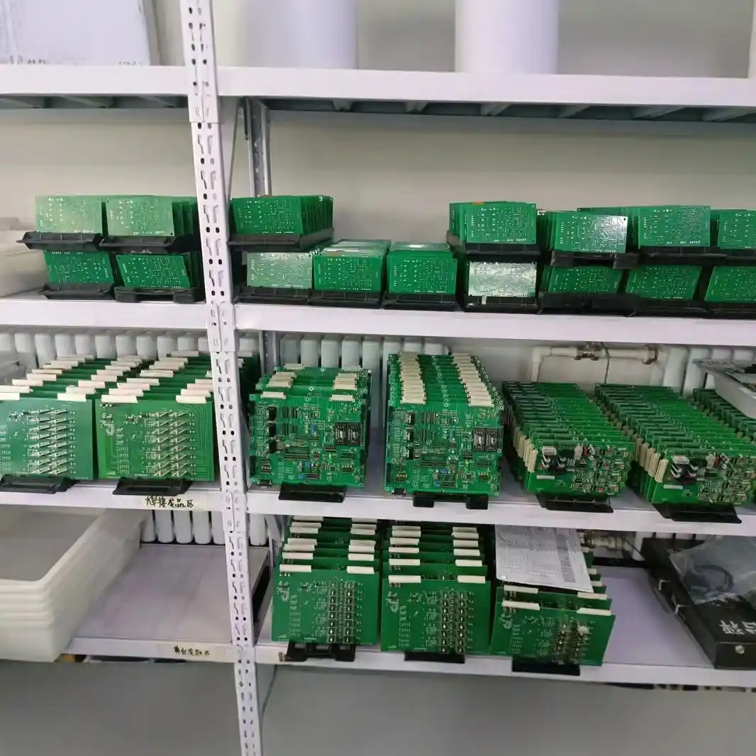
Why Do Designs That Work in Prototyping Break at Scale?
Prototype assembly is forgiving. A skilled technician compensates for pad size issues, corrects placements by hand, and applies judgment to every board. Automated production lines cannot do that. They execute the design exactly as specified — thousands of times — with no tolerance for ambiguity. When a design has hidden manufacturability problems, those problems do not disappear at scale. They multiply.
The two main reasons prototype designs fail at scale are DFM gaps and DFT gaps. DFM gaps cause the automated assembly process to produce defects. DFT gaps prevent those defects from being caught efficiently before shipment.
DFM Gaps: Why the Automated Line Produces Defects
DFM (Design for Manufacturability) is a structured review that checks whether your design can be built reliably on a real SMT production line. The following DFM problems are the most common root causes of defects in first production runs.
Layer count over-engineering. Adding layers to solve routing problems is easy at prototype stage. But moving from a 4-layer to a 6-layer PCB raises bare board cost by 30–50% in mass production. More importantly, every unnecessary layer adds process complexity that increases risk of delamination and via failure across thousands of thermal cycles.
Non-standard footprints. A technician can hand-solder a slightly inaccurate pad by eye. Pick-and-place machines need precise pad dimensions and centroid coordinates. A 0.1 mm footprint error that a technician corrects by feel becomes a systematic defect at 50,000 units — appearing on every board until the design file is corrected.
Tight component spacing. High-speed pick-and-place machines require defined clearance zones around each component. Inadequate spacing causes placement errors and limits camera access for AOI inspection after soldering. If the AOI camera cannot see a joint, that joint is not verified.
Stencil aperture mismatches. Solder paste volume is controlled by stencil aperture size. Incorrect apertures cause insufficient solder on some pads and bridging on others. At scale, this is not a random defect — it appears on every board, in the same location, until the stencil is corrected.
DFT Gaps: Why Defects Go Undetected Until the Field
DFT (Design for Testability) determines how efficiently a completed assembly can be electrically verified. A board with DFT gaps is not untestable — it is expensively testable. That difference matters enormously at high volume.
Flying probe testing can navigate almost any board design and requires no custom fixture. But it takes up to 15 minutes per board. ICT (In-Circuit Testing) with a bed-of-nails fixture completes the same test in approximately 1 minute. The fixture costs $2,000 to $10,000 to build — a one-time investment. At 50,000 units, the choice between 15 minutes and 1 minute per board is not a preference. It is a production capacity decision.
DFT review ensures that all critical signal nets have accessible test points, that BGA components include JTAG boundary scan capability, and that the board layout supports fixture pin access. A board that passes DFT review at DVT stage can be tested at ICT speeds during mass production.
The key decision: Schedule DFM and DFT reviews during DVT — with the same factory that will handle mass production. A factory reviewing designs it will assemble has a direct incentive to find problems before they become production defects.
DFM and DFT reviews can only fix problems if they happen at the right stage. A change made in early development costs hours. The same change made after production tooling is committed can cost tens of thousands of dollars. That cost gap is what the EVT–DVT–PVT framework is designed to manage.
EVT, DVT, PVT: When Is the Right Time to Fix Each Problem?
Every design has problems. The variable is not whether problems exist — it is at what stage you find and fix them.
A schematic revision in EVT takes a few hours of engineering time. The same change after PVT sign-off can mean $50,000 in scrapped inventory, re-tooled stencils, re-qualified processes, and delayed shipments. The three validation stages — EVT, DVT, and PVT — exist to define a clear window for each type of change, so teams fix the right things at the right time.
What Each Stage Is Actually For?
EVT — Engineering Validation Testing (3–50 boards)
EVT confirms that the design performs as intended under real operating conditions. Schematic changes, component swaps, thermal management revisions, and stack-up changes are all normal here. EVT ends when the board passes electrical and functional tests with no open design issues. This is the last stage where fundamental design changes are cheap.
DVT — Design Validation Testing (20–200 boards)
DVT is where the board gets industrialized. DFM and DFT reviews happen here — not before, and not after. Component footprints are finalized, regulatory certifications (CE, FCC, UL) are pursued, and the manufacturing partner joins the process. Any design changes after DVT sign-off should be minor adjustments only. The design is frozen at DVT.
This is also where ICT fixture design begins and panelization strategy is finalized — both in consultation with the production factory. Starting these in DVT means they are ready for PVT, not scrambled together during it.
PVT — Production Validation Testing (50–500 boards)
PVT runs boards using the exact production tooling, stencils, reflow profiles, and components that will be used in mass production. PVT does not validate the design — that was DVT. PVT validates the manufacturing process. A PVT pilot run achieving 98%+ first-pass yield is a green light. A PVT run with 15% rework identifies a process problem that must be corrected before committing to full volume.
| Stage | Quantity | Design Status | DFM/DFT Review | Primary Question |
|---|---|---|---|---|
| EVT | 3–50 units | Open | Not yet | Does the design work? |
| DVT | 20–200 units | Stabilizing | Yes — happens here | Can the design be manufactured at scale? |
| PVT | 50–500 units | Frozen | Complete | Does the production process hit yield targets? |
| Mass Production | 1,000+ units | Frozen | Complete | Can the factory sustain output at cost? |
The key decision: Do not compress or skip PVT under schedule pressure. A failed PVT is far cheaper than a failed production run. If PVT shows 95% first-pass yield, pushing to mass production means 5% of every board needs rework — across the entire volume. At 50,000 units, that is 2,500 rework events.
Fixing problems at the right stage keeps the design healthy. But once production begins at scale, a different system takes over: the quality control stack that runs continuously across every board on the line.
How Does Quality Control Change at Scale?
A prototype team checks boards by eye and corrects problems as they appear, but that method does not scale.
At high volume, quality control is a layered, automated defense system. Each layer targets a specific category of defect at the earliest possible point in the process — because the cost of correcting a defect rises with every step it travels down the production line uncaught.
SPI, AOI, and X-Ray: What Each Layer Does and When It Fires
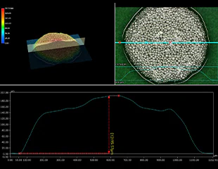
SPI — Solder Paste Inspection (fires before component placement)
SPI is the first inspection gate. A 3D machine measures paste volume, coverage area, and height at every pad immediately after solder paste printing — before any component is placed. Boards that fail SPI are pulled before the pick-and-place machine touches them.
This matters because most SMT defects — solder bridges, cold joints, insufficient solder, and component shifting during reflow — originate from incorrect paste deposition. Catching paste errors at SPI removes the root cause before any downstream process time is spent on a defective board.
AOI — Automated Optical Inspection (fires after placement and after reflow)
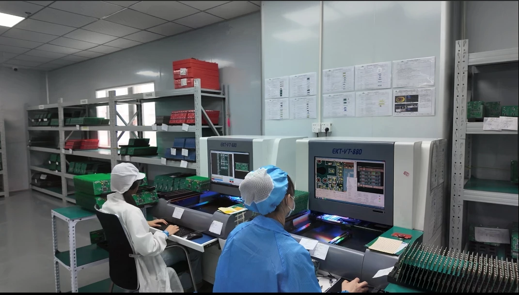
AOI uses high-resolution cameras to scan boards at two points: after component placement (checking position and polarity) and after reflow soldering (checking joint quality). It identifies missing components, reversed orientation, misaligned placement, solder bridges, solder balls, and insufficient fillets. A full AOI pass takes 10 to 20 seconds per board.
Manual visual inspection at 10,000 units per day is not viable. AOI is. And because AOI results feed back into the process — a trend of bridging on one component footprint triggers a stencil aperture review — it improves quality over time rather than just measuring it.
X-Ray Inspection (fires for BGA and QFN boards)
X-ray inspection targets solder joints that are physically hidden under package bodies — BGA balls, QFN pads, and CSP connections that no camera can see. X-ray imaging reveals voids, cold joints, bridges, and misaligned balls inside the package boundary.
In high volume production, X-ray inspection is applied to 100% of boards containing BGA or QFN components — not a sample. A missed BGA solder bridge that reaches the field generates warranty returns, root cause investigations, and customer confidence damage that costs far more than any production inspection overhead.

When to Apply Each Inspection Layer?
| Inspection Type | Trigger Point | What It Catches | When It Is Required |
|---|---|---|---|
| SPI | After paste printing | Paste volume, coverage, height errors | All high-volume SMT boards |
| Pre-reflow AOI | After pick-and-place | Component placement, polarity | Dense SMT boards |
| Post-reflow AOI | After reflow soldering | Solder joint quality, bridges, missing parts | All SMT boards |
| X-Ray (AXI) | After reflow | BGA/QFN internal joint defects | Any board with BGA or QFN components |
| ICT / FCT | After full assembly | Electrical opens, shorts, full function | High volume final verification |
Inspection catches what can be seen or imaged. But some boards pass every inspection step and still fail in operation — a misconnected net, a wrong component value, a firmware-level fault. Electrical testing is what catches these failures. The problem is that the test method used at the prototype stage becomes economically unworkable at high volume. Choosing the wrong method at scale either leaves defects undetected or creates a test bottleneck that slows the entire production line.
Which Testing Method Is Right for High Volume PCB Assembly Services?
Testing strategy is a cost decision as much as it is a quality decision. The method that works for 50 prototype boards rarely makes economic sense for 50,000 units.
Each test method has a different cost structure, a different coverage capability, and a different throughput rate. Choosing the wrong combination either leaves defective boards undetected — or destroys unit economics through test bottlenecks.
Flying Probe, ICT, and FCT: What Each One Actually Does
Flying Probe Testing
Flying probe testing uses movable electrical probes that navigate the board and contact test points without a custom fixture. It requires no upfront tooling and programs directly from CAD files. It is the correct choice for prototypes and low-volume NPI runs.
At high volume, it is not viable. One board takes up to 15 minutes. At 50,000 units, that is a single machine running for over a year of continuous test cycles — for one product. Flying probe is not a primary test method for high volume PCB assembly.
In-Circuit Testing (ICT)
ICT uses a bed-of-nails fixture — a custom-built test interface with spring-loaded pins that contact all designated test points simultaneously. A complete ICT test cycle takes approximately 1 minute per board. It verifies electrical opens and shorts, component values, JTAG boundary scan coverage, and functional sub-circuit performance.
The fixture investment of $2,000 to $10,000 is amortized quickly. At 10,000 units, a $5,000 fixture adds $0.50 per board. The time saving compared to flying probe at the same volume is enormous. ICT is the standard electrical verification method in high volume PCB assembly services worldwide.
Functional Circuit Testing (FCT)
FCT powers the assembled board and runs its actual operating firmware. It applies real input signals and measures output responses to verify that the board performs as the final product requires. No combination of ICT and AOI replaces this — ICT verifies electrical connections, but FCT verifies that the board works as a product.
FCT jig development requires input from both the engineering team and the production factory. The jig replicates the product’s actual operating interfaces. It takes time to develop, but it is the final and highest-confidence quality gate before shipment.
| Test Method | Cycle Time | Fixture Required | Volume Fit | What It Covers |
|---|---|---|---|---|
| Flying Probe | Up to 15 min/board | No | Prototype / Low volume | All nets, excellent coverage |
| ICT | ~1 min/board | Bed-of-nails ($2K–$10K+) | High volume | Opens, shorts, values, JTAG |
| FCT | Variable | Custom product jig | All volumes | Full product function |
| X-Ray (AXI) | ~30 sec/board | No (machine investment) | Medium–High | BGA/QFN internal joints |
The key decision: Build the ICT fixture during DVT, in parallel with regulatory certification testing. ICT fixture lead time is typically 2 to 4 weeks. Having it ready for PVT means test coverage is validated before mass production starts — not scrambled together after the first production run reveals gaps.
Testing strategy determines whether defective boards reach customers. But before any of this becomes relevant, the components on those boards have to actually be available — at the quantities and lead times the production schedule requires. That is the supply chain question, and it catches more teams off guard than any other part of the mass production transition.

What Happens to Your BOM and Supply Chain at Scale?
Component sourcing is where more production ramps fail than at any point in design or assembly. A BOM that handled 50 prototype boards cleanly can carry serious structural risk when it runs at 50,000 units.
BOM cost represents 60 to 70% of total PCBA cost in mass production. Component availability drives production schedule. Getting both right before production commits is an engineering and strategic decision — not a procurement afterthought.
How BOM Risk Grows With Volume?
Single-source components become schedule dependencies. A component with one manufacturer and a 20-week lead time is manageable at prototype scale. At mass production scale, it is a single point of failure that can stop an entire production line. Every single-source component needs either a pre-qualified alternate MPN or a contracted supply agreement before production starts.
Open-market sourcing introduces counterfeit risk. Prototype quantities are often sourced through brokers or spot-market traders. At high volume, this practice introduces counterfeit components — parts that pass incoming inspection but fail in the field. High volume production requires authorized distributors or incoming inspection processes, including X-ray and full electrical parameter testing.
Lead times are not predictable. Copper-clad laminate lead times extended to 16 to 20 weeks during recent supply disruptions. Certain semiconductor categories — microcontrollers, wireless modules, power management ICs — have carried allocation windows from 12 to 52+ weeks. A BOM that is fully available at 50 units may be allocation-constrained at 50,000 units.
BOM Readiness: Prototype vs. High Volume
| BOM Factor | Prototype Standard | High Volume Requirement |
|---|---|---|
| Part identification | Description + value | Manufacturer part number (MPN) required |
| Alternate parts | Not required | Pre-qualified AVL for all critical components |
| Sourcing channels | Open market acceptable | Authorized distributors only |
| Safety stock | Not required | 10% buffer on high-risk, long-lead components |
| Lead time tracking | Ad hoc | Active monitoring of allocation status |
| RoHS documentation | Optional | Required for all components |
Manufacturers that maintained 10% buffer stock on high-risk components reduced production downtime by 70% during shortage events. For a 50,000-unit run, a 10% buffer on a $0.50 component costs $2,500. An unplanned production stoppage waiting for allocation costs far more than that in a single day.
Supply chain risk determines whether production runs on schedule. Cost structure determines whether it runs at the margins your product needs. The two are connected — and both are shaped significantly by where production happens and who manages it.
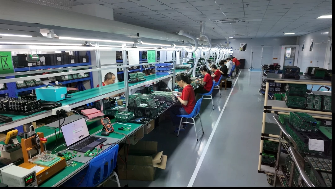
What Actually Drives Cost in High Volume PCB Assembly — and What Can You Control?
Cost per unit in high volume PCB assembly is not a number a supplier gives you. It is the output of engineering decisions, process choices, and procurement strategy — most of which are made before a single board is built.
Understanding what drives cost changes the questions you ask before accepting a quote. It also gives you real levers to pull — not just negotiation on margin.
The Three Cost Buckets
BOM Cost: 60–70% of total PCBA cost
Components dominate PCBA cost in mass production. Engineering decisions that reduce BOM cost include choosing standard commercial packages over proprietary formats, specifying multi-source components, and consolidating circuit functions to reduce component count. None of these changes is free at the prototype stage — but each one compounds in value across 50,000 units.
PCB Fabrication Cost
Layer count is the most powerful cost multiplier in board fabrication. Moving from 4 to 6 layers increases bare board cost by 30 to 50%. Adding HDI features — blind vias, buried vias, microvia stackups — increases cost further. DFM optimization at the minimum viable layer count has a direct, measurable cost impact at high volume.
Surface finish choices also affect both cost and quality. ENIG (Electroless Nickel Immersion Gold) provides reliable solderability for fine-pitch SMT and long shelf life, but costs more than HASL. The right finish depends on component mix and IPC class requirement — not a default preference.
Assembly and Test Cost
SMT assembly is highly automated and cost-effective at scale. Through-hole and mixed-technology boards cost more per unit because they require sequential processing. Testing cost — ICT fixture amortization, FCT jig investment, X-ray machine time — decreases per unit as volume increases. A $5,000 ICT fixture across 50,000 units is $0.10 per board.
Panelization: The Efficiency Multiplier Most Teams Overlook
Panelization groups multiple individual PCBs onto a larger substrate array for simultaneous processing through the SMT line. A panel of 6 boards reduces machine passes to one-sixth per board for every step from paste printing through reflow — directly reducing cycle time and per-unit cost.
Panelization must be designed, not assumed. V-scoring handles boards with straight edges. Tab routing handles irregular shapes. Fiducial markers, breakaway tab dimensions, and rail widths must match the production line’s conveyor specifications. The right time to finalize panelization is during DVT, in consultation with the production factory — not during PVT when tooling is already being committed.
Saving $0.05 per unit through DFM optimization at 50,000 units is a $2,500 reduction. Saving $0.20 per unit is $10,000. These numbers compound across product generations — which is exactly why front-loaded engineering investment in DFM pays back faster than any other cost reduction activity.
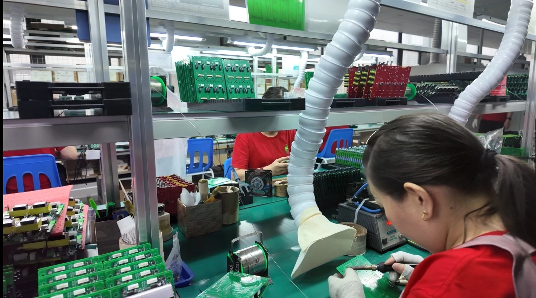
Why Do B2B Teams Choose a Shenzhen PCB Assembly Factory for Volume Production?
Choosing a manufacturing location for high volume PCB assembly is a strategic decision — not just a cost comparison. The right answer depends on what your design requires, what your supply chain needs, and what your quality standards mandate.
Shenzhen’s advantage in high volume PCB assembly is structural. It is built from 40+ years of integrated supply chain development — not just lower labor cost. Understanding what that means in practice helps procurement teams ask the right questions when evaluating suppliers.
What Shenzhen Offers That Other Locations Do Not Replicate at Scale
Component sourcing speed. Shenzhen hosts Huaqiang North, the world’s largest electronic components distribution center. Complete BOM sourcing that takes 22 hours in other global markets takes approximately 1 hour locally. This compression directly reduces production scheduling delays and material holding cost at high volume.
Manufacturing technology depth. Leading Shenzhen factories use LDI (Laser Direct Imaging) for fine-line circuitry, high-precision CNC drilling, full MES (Manufacturing Execution System) integration, and AI-assisted AOI inspection. These are not marketing claims — they are process capabilities that affect yield rates and lead times on complex, dense designs.
Cost competitiveness at industrial scale. Shenzhen PCB fabrication costs range from approximately $0.10 to $0.20 per square inch, compared to $0.30 to $0.60 per square inch in the United States. This reflects both labor and integrated supply chain advantages that remain even as overall manufacturing costs in China rise.
Certification coverage for regulated industries. Factories serving global B2B markets hold ISO 9001:2015 for general quality management, IATF 16949 for automotive supply chains, ISO 13485 for medical device manufacturing, and IPC-A-610 certified inspection personnel. These are audit requirements for regulated industries — not optional credentials.
China accounts for more than 50% of global PCB production capacity. Shenzhen is its primary manufacturing core. For high volume PCB assembly at industrial scale, Shenzhen is not merely competitive — it is the benchmark against which all other options are evaluated.
What About PCB Reverse Engineering for High Volume Production?
Not every high volume program begins with a new design. A significant number of B2B manufacturing programs start from a physical board — with no original engineering files available.
PCB reverse engineering is the process of converting a physical circuit board assembly into a complete set of production-ready engineering documents — Gerber fabrication files, a full BOM with current manufacturer part numbers, and a recovered schematic. The output is functionally identical to a clean-sheet design. It feeds directly into PCB fabrication and high volume PCBA production with no difference in the manufacturing workflow.
When Reverse Engineering Is the Right Path?
The most common scenarios where reverse engineering enables high volume production are:
Legacy industrial equipment. The original manufacturer no longer exists or no longer supports the product. Replacement boards are needed to keep installed equipment running. Reverse engineering provides fabrication and assembly files to produce replacement boards from any qualified factory.
Acquired product lines. A company acquires a product range but the engineering files were not part of the transaction. Reverse engineering reconstructs the full technical package from physical hardware.
Obsolete component re-specification. The original design used components that are now end-of-life. The reverse engineering and BOM reconstruction phase identifies currently available equivalent parts and rebuilds the BOM for production using modern components.
| Reverse Engineering Output | Description | How It Enters Production |
|---|---|---|
| Gerber files | Layer-by-layer PCB fabrication data | Direct input to PCB fabrication line |
| BOM with MPNs | Full component list with current part numbers | Procurement and assembly line programming |
| Schematic | Recovered circuit diagram | Design review and modification capability |
| Centroid file | Component placement coordinates | Pick-and-place machine programming |
| Firmware (if required) | IC data extracted from programmable devices | Functional duplication of original board |
FAQ: High Volume PCB Assembly
What is the minimum quantity for high volume PCB assembly?
Most factories define high volume as 1,000 units or more per production run. Some set the threshold at 10,000 units. The more meaningful measure is total component placements — volume that justifies dedicated ICT fixtures, custom stencils, and automated line programming falls into the high volume category regardless of exact board count.
When should I freeze my PCB design before mass production?
The design should be frozen at the end of DVT — before PVT begins. Changes after PVT sign-off require re-qualification of production tooling, re-testing, and potentially scrapping produced inventory. Changes during EVT and DVT are normal. Changes after PVT are expensive.
Is flying probe testing acceptable for high volume PCB assembly?
Flying probe is appropriate for prototypes and low-volume NPI runs. For production runs above 1,000 units, ICT with a bed-of-nails fixture is the standard choice. Flying probe takes up to 15 minutes per board. ICT takes approximately 1 minute. The economic difference at scale is not a preference — it is a production capacity constraint.
What certifications should I verify before selecting a PCB assembly services provider?
At minimum: ISO 9001:2015, IPC-A-610 certified inspection personnel, and RoHS compliance documentation. For specific industries: IATF 16949 for automotive, ISO 13485 for medical, AS9100D for aerospace. Confirm certifications are current and subject to annual third-party audit — not just historical claims on a company profile page.
How does a one-stop PCB assembly partner reduce production risk?
When design, fabrication, component sourcing, SMT assembly, and testing are managed by one team, engineering changes propagate through all process stages simultaneously. DFM issues found during review are corrected by the same team that will run production. Accountability for first-pass yield is unified — not distributed across multiple vendors with competing priorities.
What makes a BOM ready for high volume production?
A production-ready BOM must include manufacturer part numbers (MPN), approved alternative part numbers (AVL), reference designators that exactly match the PCB layout, package and footprint specifications, RoHS compliance status, and quantity per board. A BOM with only descriptions and values is adequate for prototyping. It is not adequate for high volume procurement and automated assembly line programming.
What is the role of PCB reverse engineering in high volume production?
Reverse engineering converts a physical board into Gerber files, BOM, and schematic — the full engineering package needed for PCB fabrication and PCBA assembly. Once complete, the output enters the standard production workflow with no difference from a new design. It is the required pathway for legacy hardware, acquired product lines, and boards whose original engineering files no longer exist.
IWDF Solutions — Shenzhen, China | One-Stop PCB Design, Reverse Engineering, PCB Manufacturing & High Volume PCB Assembly Services
Contact us to discuss your production requirements.

