

Reverse Engineering can be applied to most PCB types—from single-layer and double-layer boards to many multilayer designs—but complexity, cost, and risk increase significantly as layer count, density, and special materials increase. This guide explains which boards are realistic to reverse engineer, what to expect in terms of effort and timeline, and when to partner with a professional factory like IWDF Solutions.
What Is PCB Reverse Engineering?
PCB reverse engineering is the step-by-step process of working backwards from a finished circuit board to figure out exactly how it was designed and how it works. Think of it like reverse-baking a cake: you have the final cake (the physical PCB), and you carefully analyze it to recreate the recipe (the design files and documentation).
It’s more than just copying. It’s a full investigation to recover the original designer’s intent and create a clear, usable set of instructions for building or, more commonly, repairing it again.
Here’s how it’s done, step by step:
- Parts Inventory: First, you identify and write down every single component on the board (chips, resistors, connectors, etc.), like making a detailed parts list.
- Trace the Map: Then, you carefully follow all the copper traces on the board to see how every part is connected. This is like tracing all the roads on a map to understand how cities are linked.
- Draw the Schematic: Using that connection map, you draw the circuit diagram (schematic) from scratch in computer software. This is the “blueprint” or the instruction manual of how the circuit functions.
- Rebuild the Layout: Next, you recreate the physical board itself in design software—where each part sits and how the copper pathways are routed between them.
- Test and Confirm: Finally, you build a prototype from your new design and test it to make sure it works exactly like the original board.


Why do companies and individuals actually do this?
In the real world, reverse engineering most often starts with a simple, urgent problem: a critical piece of equipment breaks down, but the manufacturer has stopped making it or supporting it. Buying a new, different machine could cost a fortune or disrupt operations. Reverse engineering provides a solution.
Beyond that core need, it solves three common business problems:
- Fixing and Supporting “Unsupported” Equipment: This is the most frequent reason. When a machine fails and you can’t get spare parts, original schematics, or help from the original maker, reverse engineering lets you open the “black box.” You can figure out the failure, rebuild the broken board, and get the equipment running again for a fraction of replacement cost.
- Keeping Old Products Alive: Sometimes the original design files are lost, the company that made it doesn’t exist anymore, or critical parts are no longer sold. Reverse engineering rebuilds the documentation so you can repair, support, or manufacture the product again.
- Improving an Old Design: Instead of designing a whole new board, you can start with a reverse-engineered version of an old one. Then you can upgrade it—swap in newer parts, fix known issues, or improve its performance—saving huge amounts of time and money.
- Moving Production: When a product needs to be manufactured in a new factory (especially in a different country), the new factory needs perfect instructions. Reverse engineering creates those instructions, ensuring the new factory can build an identical product.
What Types of PCB Boards Can Be Reverse Engineered Successfully?
Almost any PCB can be reverse engineered in theory, but in practice, the effort, tools, equipment requirements, and risk profile differ dramatically between single-layer boards, basic double-layer PCBs, and dense multilayer or HDI designs.
Single-Layer PCBs – Low Cost, Low Risk
Single-layer boards are the straightforward reverse engineering target. All copper traces are visible on one surface; components are through-hole mounted on the opposite side. A high-resolution photograph, continuity testing with a multimeter, and basic CAD work can recover the complete netlist and layout within days. These projects typically cost low and take 3–7 working days. Suitable for rapid board recreation when documentation is missing.

Double-Layer PCBs – Still Very Feasible
Double-layer boards require more detailed two-sided photography, methodical tracing, and careful layer mapping, but remain highly cost-effective reverse engineering candidates. With plated through-holes connecting both surfaces, standard industrial control boards and consumer electronics fall into this category. Projects typically run middle cost with 1–3 week timelines. Most manufacturers’ bread-and-butter work includes double-layer boards for industrial applications.

Simple Multilayer (4–6 Layers) – Feasible with Professional Tools
Four-to-six-layer boards with moderate component density and common materials (FR-4, standard blind/buried via counts) can be reverse engineered, but require non-destructive X-ray inspection or destructive delayering, specialized test equipment, and deeper analysis. Internal layers must be mapped through layer-by-layer imaging. Costs escalate to higher than double-layer pcb reverse; timelines extend to 3–8 weeks depending on complexity. These represent the threshold where professional factory infrastructure becomes necessary.

Complex Multilayer & HDI – Case-by-Case Assessment Required
Boards with 8+ layers, dense BGA packaging, multiple blind/buried via patterns, high-speed differential routing, controlled impedance requirements, or specialized materials (RF substrates, thick copper, flex/rigid-flex) can be reverse engineered, but require detailed feasibility evaluation. Success depends on technical feasibility, legal compliance, customer expectations regarding design fidelity, and risk tolerance. Costs highest; timelines extend 8–16+ weeks. Requires an explicit go/no-go decision by both the customer and the manufacturer.

Single-Layer PCBs: When Reverse Engineering Is Straightforward
Typical Characteristics
Single-layer PCBs consist of a single copper trace layer laminated to a substrate, with components soldered primarily through plated through-holes on the opposite side. Trace widths are typically 8–10 mils or wider; spacing between traces is usually generous. These boards rarely incorporate vias except as component mounting holes. Component density is deliberately low, making traces easy to follow visually or with basic continuity testing.
Why Single-Layer Boards Are Easy to Reverse Engineer?
Straightforward visibility is the primary advantage. Unlike multilayer designs where internal routing is hidden, every trace on a single-layer board is directly accessible to visual inspection and tracing. The netlist can be reconstructed by photographing the board, identifying component connections, and validating continuity using a simple multimeter.
Modern smartphone cameras produce photographs with sufficient resolution (8–12 megapixels) to capture trace width, component pad positions, and routing clearly. Combined with basic measurement tools and free PCB CAD software, a competent technician can complete schematic extraction manually in a single working day for boards with fewer than 100 components.
Typical Use Cases
Single-layer boards commonly appear in consumer appliances (microwave timers, refrigerator control modules), small LED drivers, simple power supplies, basic industrial sensors, communication interface modules, and legacy industrial equipment where replacement inventory has dried up. Many of these products were designed 10–20 years ago, when multilayer boards were unnecessary for their electrical requirements.
What IWDF Solutions Does for Single-Layer Projects
For single-layer reverse engineering, IWDF Solutions follows a streamlined process: initial board analysis and documentation, high-resolution multi-angle photography, manual netlist extraction and schematic recreation using industry-standard CAD tools, BOM compilation with modern component cross-references where original parts are obsolete, and Gerber file generation for prototype fabrication. Typical turnaround is 5–10 working days. The reconstructed design then moves directly to prototype PCB fabrication and basic functional testing (power-on, signal continuity, thermal operation if applicable). Upon validation, boards proceed to small-lot production (10–500 units) or full manufacturing scaling. This one-stop-shop approach eliminates vendor handoff delays and communication gaps that plague customers trying to coordinate multiple service providers.
Double-Layer PCBs: The “Sweet Spot” for Reverse Engineering
What Makes Double-Layer Boards Different?
Double-layer PCBs feature conductive copper on both the top and bottom surfaces, connected by plated through-holes (vias). Components are typically mixed: surface-mount devices on one side (often the top), through-hole components on the other. This allows significantly higher component density than single-layer designs while maintaining manufacturing simplicity and cost.
Traces can now route around obstacles by transitioning between layers, increasing design flexibility. Internal power and ground planes become feasible, though not yet common, in basic double-layer work. Via patterns indicate layer transitions and provide key clues to the designer’s intent.
Reverse Engineering Workflow for Double-Layer PCBs
The process begins with multilateral board documentation: high-resolution photographs of both the populated and bare board (after component removal), note-taking on component placement, orientation, and any visible markings or rework areas. Second, external layer analysis: tracing top-layer copper, identifying via locations and designators, and recording all connections to component pads. Third, bottom-layer tracing: repeating for the bottom side, carefully noting which traces connect to vias linking to the top layer.
Fourth, layer connectivity mapping: using a multimeter’s continuity function to validate connections assumed and probe critical nets (power rails, ground returns, signal lines). A continuity tester typically emits an audible tone when two probed points are connected by a trace, speeding validation during manual tracing. Fifth, schematic reconstruction: drawing the complete circuit in CAD, cross-referencing component datasheets to validate pin assignments and functional logic.
Finally, BOM and Gerber generation: compiling a final bill of materials with designators, footprints, and modern component substitutes; exporting layered PCB layout as Gerber files for prototype fabrication.
Common Challenges and How Professionals Solve Them
Challenge 1: Ground and Power Distribution
Modern double-layer boards often include poured copper ground zones or partial ground planes for current return paths. These large copper regions are difficult to trace visually or with a continuity tester because the copper itself has near-zero resistance. Professional factories address this by photographing at extreme angles to reveal trace boundaries, using trace-width measurements and design heuristics (e.g., “larger copper often indicates power or ground”), and referencing test points or via patterns that hint at plane locations. X-ray inspection is not yet necessary, but high-resolution photography with controlled lighting is essential.
Challenge 2: Buried Vias and Via Masking
Some manufacturers solder-mask over vias, making them invisible to the naked eye. A multimeter probe will not register them reliably. Solution: Remove the solder mask chemically or mechanically (careful abrasion with fine sandpaper or specialized chemical strippers), then photograph or probe. This is destructive but necessary if the via pattern is unclear.
Challenge 3: Component Package Identification
Surface-mount resistors and capacitors often lack readable markings, especially tiny 0402 packages. Many parts have been obsoleted or replaced. Professional engineers maintain extensive component libraries indexed by footprint and schematic context (e.g., “capacitor between Vcc and ground, near IC pin 32 → likely a bypass capacitor, probably 0.1 µF”). They cross-reference datasheet pinouts, voltage ratings, and circuit topology to narrow candidates. When exact part numbers are unreadable, they substitute modern equivalents with identical or superior specifications.
Challenge 4: Incomplete or Reworked Traces
Production rework (added wires, scratched traces, resoldered joints) leaves an ambiguous board state. Solution: Accept that the physical board may be a variant or rework build and document it as such. Cross-reference with component BOM to infer the “intended” state. If multiple boards are available, compare them to reconstruct the production baseline.
When Double-Layer Projects Are a Good Fit for IWDF Solutions?
Double-layer reverse engineering is IWDF Solutions’ bread-and-butter offering for industrial clients needing legacy board support. Whether you’re an OEM whose supplier closed, an equipment refurbisher seeking cost-effective parts, or an engineer upgrading an aging control system, double-layer boards represent an ideal cost-to-feasibility ratio. IWDF has completed hundreds of such projects for industrial automation, power supplies, sensors, and telecommunications equipment. The typical project cost ($1,200–4,000) and two-to-three-week timeline fit comfortably within most product-support budgets. IWDF’s integration of design, prototyping, and small-batch manufacturing means you can move from reverse engineering to production-ready inventory without external vendor coordination.
Standard Multilayer PCBs (4–6 Layers): Feasible with the Right Tools
What Counts as a “Standard” Multilayer Board
Four-to-six-layer boards are the industry standard for modern industrial control electronics, automotive subsystems, communications modules, and intermediate-complexity consumer devices. They employ common FR-4 glass epoxy substrate, standard copper weights (1–2 ounces per square foot), plated through-holes for power and signal, and a small number of blind or buried vias concentrated around high-density BGA packages or fine-pitch component areas.
Impedance control may be present (defined trace widths and spacing near high-speed digital signals), but is not yet mission-critical as it would be in RF or high-speed memory applications. Power distribution uses dedicated ground planes and often a power plane, reducing EMI and improving current delivery.
Why Reverse Engineering Gets Harder
The fundamental challenge: inner layers are invisible. Unlike single or double-layer boards, where all copper is directly accessible, a 4-layer board contains two or more internal copper layers hidden within the substrate laminate. Visual inspection and simple continuity testing cannot reach them.
Internal routing must be inferred or extracted using mechanical or imaging techniques. A 4-layer stack-up might look like: top layer (signals/components), inner layer 1 (power plane), inner layer 2 (ground plane), bottom layer (signals/components). Without breaking the board apart, you cannot directly see the routing on inner layers 1 and 2.
Additionally, signal integrity considerations (impedance, crosstalk, propagation delay) become important. Trace widths and spacing are no longer arbitrary but carefully controlled. Ground and power plane purity (unbroken copper with minimal via cutouts) is critical. Simply copying layout dimensions without understanding these constraints risks design failure.
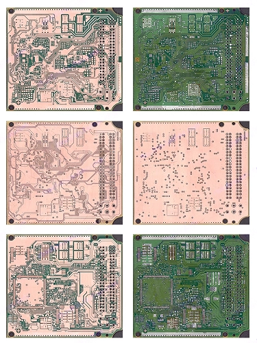
Techniques Professionals Use
Non-Destructive X-Ray Imaging
X-ray tomography (3D X-ray or CT scanning) captures the internal layer structure without disassembly. Equipment shoots X-rays through the board from multiple angles, collecting 2D radiographic images. Mathematical reconstruction algorithms assemble these 2D images into a 3D model showing layer positions, via holes, BGA ball attachments, and internal routing.
Professional-grade X-ray systems cost $50,000–300,000 but are now common in PCB failure analysis laboratories and contract manufacturers. Scanning a typical 4-layer board takes 15–45 minutes; image processing and reconstruction add another hour. Output is a 3D point cloud or volumetric dataset that technicians can examine layer by layer.
Advantages: non-destructive (board survives), reveals internal details at micrometer resolution, no hidden traces. Disadvantages: high equipment cost (outsourcing to a service lab costs $500–1,500 per scan), exterior components must be removed if they obscure internal vias, very high-density boards (8+ layers, tight via patterns) can produce ambiguous reconstructions if pixel resolution is insufficient.

Destructive Delayering
Alternative technique: physically remove material between layers while photographing each layer. Solder mask is removed chemically or mechanically. The board is then precisely ground down by 10–50 mils, photographed at high resolution, and grinding is repeated to expose the next layer.
Methods include: manual sandpaper (very slow, ~1 layer per day, high waste risk), CNC surface grinder (20–60 minutes per layer, precise depth control), or abrasive jet (waterjet or powder-jet abrading, 30–90 minutes per layer, gentler on copper).
After each layer exposure, a high-resolution scanner (3200+ DPI) captures the copper traces, via pads, and component footprints. Technicians compile the layer-by-layer images into a complete PCB model.
Advantages: reveals routing with maximum clarity, exposing hidden vias, trace widths, and connections directly. Disadvantages: destructive (board cannot be reused), time-consuming (4 layers = 4–8 hours of machine time plus manual work), material waste, risk of substrate cracking if controlled improperly, requires a second board sample for functional testing.
Hybrid Approach: X-Ray + Targeted Delayering
Many professional labs combine both techniques. X-ray provides the overall layer plan and via positions. Selective delayering is then applied only to areas of interest (e.g., around a BGA, near high-speed traces) where routing is unclear from X-ray alone. This reduces time and risk compared to full delayering.
Risk Factors
- Component obsolescence: parts may be 5+ years old and discontinued. Substitution must maintain footprint, pinout, and electrical compatibility.
- Incomplete documentation: if a board is a prototype, engineering sample, or production variant, the “final” design may be unclear. Multiple board samples help clarify revisions.
- Rework or design changes: many boards in the field have been modified. Reverse engineering captures the physical state, not necessarily the original intent.
- Validation complexity: once the design is reconstructed, prototypes must be built and functionally tested. Signal integrity or EMI issues may require iterative design tuning.
IWDF Solutions approaches these risks by requesting multiple board samples (minimum 2–3 for complex projects), conducting preliminary X-ray assessment before committing to delayering, engaging customer technical teams early to clarify design intent, and budgeting prototype validation as a separate phase before production sign-off.
When 4–6 Layer Projects Are a Good Fit for IWDF Solutions?
Industrial customers with aging control systems, automotive electronics manufacturers facing end-of-life support, telecommunications OEMs migrating production, and equipment makers needing cost-effective legacy part inventory often turn to 4–6 layer reverse engineering. The level of technical depth—requiring X-ray labs, precise CAD expertise, and manufacturing infrastructure—makes this work suitable for established factories rather than freelance designers. IWDF has completed projects for PLC controllers, power supplies, sensor modules, and communication adapters, typically requiring 4–8 weeks and costing $5,000–15,000 from reverse engineering through first-article samples. Customers benefit from integrated design validation and manufacturing readiness, avoiding the bottleneck of coordinating separate design and prototyping vendors.
Complex Multilayer, HDI, RF, and Special Boards: When Is Reverse Engineering Realistic?
Boards That Are Technically Possible but Challenging
Reverse engineering remains theoretically possible for boards with 8+ layers, dense BGA (Ball Grid Array) packages, multiple blind and buried via patterns, high-speed differential pair routing, controlled impedance requirements, or specialized materials (RF substrates, polyimide flex, metal-core for thermal management). However, “possible” does not always mean practical or cost-effective.
Blind Vias are through-holes that start at an outer layer and terminate in an inner layer, with one end open. Buried Vias connect only inner layers, completely hidden from outside view. These structures are common in high-density boards to maximize signal routing and minimize layer count. Tracing them requires either an X-ray capable of micrometer resolution or complete destructive delayering.
BGA Packages present extreme density challenges. Hundreds of solder balls arranged in a grid under a plastic package make it impossible to visually trace connections to internal board routing. X-ray is essential, but the sheer number of interconnections (300–1000+ balls on large BGAs) multiplies the netlist extraction effort.
Controlled Impedance means trace widths, spacing, and layer stack-up are precisely engineered to maintain specific electrical impedance (e.g., 50 Ohm differential pairs for high-speed serial buses, or 75 Ohm single-ended for video). Copying the physical layout without understanding the impedance stack-up often fails because the original board’s dielectric thickness, copper weight, or material properties may not be available and cannot be inferred from Gerber files alone.
High-Frequency RF Boards (2+ GHz) require attention to trace routing, via placement, and ground connectivity at levels that far exceed what visual inspection can capture. Antenna coupling, transmission line effects, and shielding become critical. Reverse engineering can map the physical layout, but reproducing RF performance often requires tuning and measurement by RF specialists.
Flex and Rigid-Flex Boards add material complexity: polyimide substrate, dynamic flex regions, adhesive layers, and specialized solder masks. Delayering destroys the flex material properties, making destructive reverse engineering unsuitable.

Key Constraints
Equipment and Infrastructure
Micrometer-resolution X-ray (micro-CT or nano-CT) costs $200,000+. Outsourcing to specialized labs adds $2,000–5,000 per scan, plus weeks of scheduling. Automated layer imaging (CNC grinding + high-speed scanning) requires capital investment that many factories lack. Specialized test equipment (RF probes, impedance meters, time-domain reflectometers) is required for validation.
Cost Escalation
Comprehensive reverse engineering of an 8-layer BGA board can easily exceed $20,000–50,000 or more. If board complexity requires iterative design cycles (prototypes, validation, tuning), the total project cost may reach $75,000–150,000. These figures are sustainable only if production volumes justify the engineering investment (typically 1,000+ units annually).
Feasibility Uncertainty
As complexity increases, perfect reproduction becomes theoretically impossible. A complex HDI board may have been designed using proprietary simulators, fine-tuned through measurement and iteration over months. Reverse engineering captures the final physical state but may not capture all design intent, optimization details, or failure-mode protections that were iterated away during original development. The reconstructed design may be functionally equivalent but not electrically identical in all operating conditions.
How Professional Factories Decide “Go” or “No-Go”?
IWDF Solutions uses a structured feasibility assessment for complex projects:
Step 1: Compliance and Intent Review
Is the reverse engineering request aligned with legitimate business needs (legacy support, end-of-life manufacturing, internal redesign)? Are there patent or trade-secret concerns? This conversation with the customer is non-technical but legally essential.
Step 2: Technical Feasibility Audit
- Board layer count and via complexity: how many internal layers, blind/buried via density, via aspect ratios?
- Component packaging: BGA ball count and pitch, number of discrete components, package size distribution.
- Special materials or processes: RF substrate, flex regions, thick copper, exotic finishes?
- Availability of reference documentation: do you have partial schematics, BOM, design notes, or only the physical board?
- Quantity of samples available: can we sacrifice boards for delayering, or must we rely on non-destructive X-ray?
Step 3: Cost-Benefit Analysis
- Estimated reverse engineering cost (based on complexity, method, and timelines).
- Estimated production volume (to assess amortization of engineering cost).
- Customer’s budget and timeline constraints.
- Risk factors (component availability, design validation cycles, potential rework).
Step 4: Technical Decision
IWDF may recommend:
- Full Go: Complete reverse engineering with both X-ray and delayering, full design validation, and confidence in first-article samples. Typical for boards with 4–6 layers, moderate density, and clear customer commitment.
- Conditional Go: Reverse engineering of primary signal nets and power distribution, with simplified handling of secondary features or analog sections. Design validation is more extensive. Suitable for boards where 80% fidelity is acceptable (e.g., refurbishment use cases where 100% performance matching is not critical).
- Redesign Instead: Recommend that the customer provide functional specifications instead of insisting on 100% layout replication. IWDF designs a new board from scratch that meets the performance target, potentially with cost and form-factor improvements. Often faster and more cost-effective than complex reverse engineering.
- No-Go: Recommend against the project due to cost-benefit misalignment, technical risk, IP concerns, or inadequate sample availability. This is infrequent but honest assessments protect both factory and customer from cost overruns or failed projects.
When You Should Consider Redesign Instead of One-to-One Cloning
Redesign becomes attractive in several scenarios:
Legacy Architecture with Obsolete Components
The original board uses discontinued ICs, outdated discrete transistors, or EOL connectors. Rather than painstaking reverse engineering followed by part substitution, a ground-up redesign using current-generation components often costs 30–40% less and delivers superior performance, thermal management, and reliability.
Thermal Performance Issues
Older boards often have suboptimal thermal layouts or inadequate heatsinking. Reverse engineering and exact replication preserve the thermal limitation. Redesign allows copper-area optimization, thermal via placement, and potential use of aluminum-core or copper-core substrates for improved heat dissipation.
Compliance or Safety Upgrades
Boards designed 10–15 years ago may not meet current EMC directives, RoHS/WEEE requirements, or electrical safety standards. Reverse engineering produces a compliant variant (switching to lead-free solder, removing restricted substances), but redesign allows optimization for modern standards during layout (e.g., improved grounding for EMC, better isolation for safety-critical circuits).
Cost Reduction Opportunity
A working board from 2010 may have been expensive to design and manufacture then. Today’s PCB processes, component costs, and EDA software often enable equivalent functionality on a simpler board (fewer layers, smaller form factor, cheaper materials). Redesign trades engineering cost against recurring manufacturing savings.
In each case, IWDF’s engineering team engages with customers to clarify whether the goal is true legacy replacement (1:1 reproduction for spares inventory) or functional equivalent upgrade (improved derivative). This conversation sets realistic scope and cost expectations.
Key Factors That Decide Reverse Engineering Difficulty
A decision framework for assessing your board and understanding its reverse engineering profile:
| Factor | Impact | Assessment |
|---|---|---|
| Layer Count | Single/double layer = easy; 4–6 = moderate; 8+ = complex | Check the board cross-section or X-ray. Blind/buried vias increase RE effort by 3–5×. |
| Via Types | Through-hole vias = visible; blind/buried = hidden. | The presence of BGA dramatically increases X-ray need. |
| Component Density | Sparse = easy to trace; high-density = difficult. | Measure component-pad area vs. board area. >70% coverage suggests complexity. |
| BGA Packages | Review PCB markings or ask the customer about max signal frequencies. >100 MHz suggests controlled impedance. | Count BGA packages and ball count. Single 400-ball BGA = 2–3 days of X-ray + image processing. |
| High-Speed Signals | Low-speed digital or analog = simple; GHz-range differential = complex. | Review PCB markings or ask customer about max signal frequencies. >100 MHz suggests controlled impedance. |
| Controlled Impedance | Not controlled = straightforward routing; controlled = design intent matters. | Presence of controlled trace widths, ground fills, or via stitching suggests impedance control. |
| RF or Analog Circuits | Digital-only = straightforward; RF = complex. | Presence of shielded sections, specialized connectors, or balun symbols indicates RF. |
| Material Specialty | Standard FR-4 = common; polyimide, metal-core, high-Tg = complex. | Check substrate color, markings, and supplier specs. Exotic materials limit replaceability. |
| Documentation Available | Complete schematic/BOM = easiest; physical board only = hardest. | Request any existing documentation. Even partial schematics reduce RE time by 30–50%. |
| Sample Availability | Multiple identical samples = safer; single unique board = risky. | Confirm you can sacrifice board(s) for delayering if X-ray is insufficient. Minimum 2 samples recommended for complex projects. |
Scoring Approach: For each factor, rate complexity as Low, Moderate, or High. If 6+ factors are “High,” the project moves into the complex-feasibility category. If 3–5 factors are “High,” the project is moderate but doable with professional infrastructure. If fewer than 3 factors are “High,” the project is straightforward and suitable for rapid turnaround.
What a Professional Reverse Engineering Project Looks Like (End-to-End)
Understanding the workflow demonstrates how IWDF Solutions adds value at each step:
Phase 1: Feasibility Assessment and Quotation (3–5 Days)
Customer Initiation
You submit physical board sample(s), high-resolution photographs, any partial documentation (schematic, BOM, design notes), and a statement of intended use (spares inventory, redesign basis, cost optimization, etc.).
IWDF Solutions Preliminary Analysis
The engineering team performs visual inspection, layer-count estimation (cross-section examination if needed), component identification, and a preliminary X-ray or delayering cost estimate.
Feasibility Report and Quote
Delivery of detailed feasibility report covering: identified board characteristics (layer count, component package types, materials), estimated reverse engineering method and timeline, itemized cost breakdown (X-ray, CAD labor, prototype fabrication, testing), risk factors and mitigation approaches, and recommended alternatives (full RE vs. partial RE vs. redesign).
Quote validity: typically 30 days, subject to no changes in project scope.
Phase 2: Data Capture and Documentation (10–30 Days)
Physical Board Preparation
- Detailed multi-angle photography of populated and bare boards.
- Selective component removal if they obscure via patterns or layer transitions.
- Careful solder-mask documentation (markings, test points, text labels).
- Serial number and revision tracking to distinguish board variants.
Non-Destructive Imaging
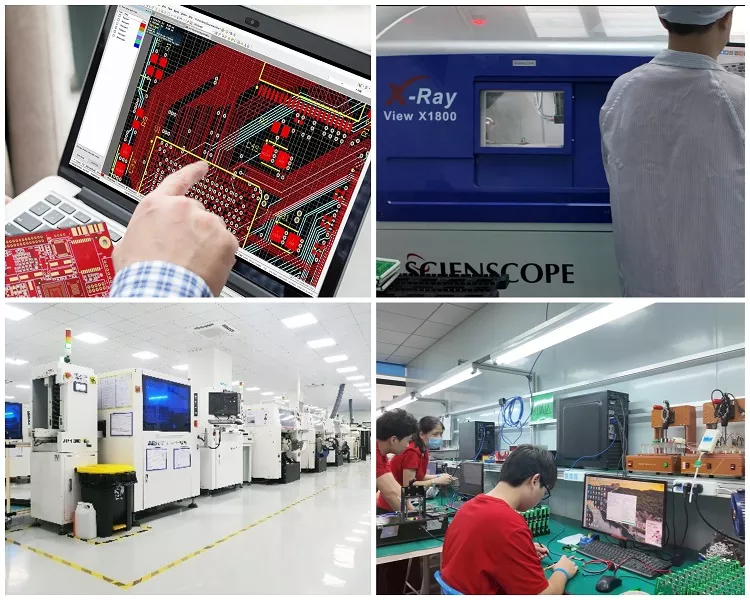
If X-ray analysis is planned, boards are analyzed using our in-house X-ray equipment. They are scanned at an appropriate resolution for layer visualization and via mapping. The resulting 3D reconstructed images are then delivered to the IWDF design team.
Destructive Delayering (if applicable)
If full internal routing visibility is required and X-ray is insufficient, CNC grinding is performed incrementally, layer-by-layer photography at 3200+ DPI follows each grinding pass, and copper trace continuity and via position are documented for each layer.
Component Identification
All ICs, connectors, and large discrete components are identified by part number. Datasheets are fetched from manufacturer sites or a cached library. Pinout mapping is documented. Obsolete parts are noted, and modern substitutes are researched (footprint compatibility, electrical equivalence, lead time, cost).
Netlist Extraction
Layer-by-layer tracing, via-connection mapping, and net-by-net documentation. For multilayer boards, each signal name (CLK, DATA, GND, VCC, etc.) is assigned to physical traces and validated against component pinouts and functional logic.
Schematic Creation
CAD drawing of complete circuit, organized by function (power, clock generation, processor section, memory, I/O, etc.). Component designators (U1, C5, R23, etc.) match physical board. Cross-referencing ensures no dangling nets or unconnected pins.
Output Deliverables
- PDF schematic diagram (professional format, suitable for documentation).
- CAD source files (e.g., PSPICE netlist, LTspice schematic).
- BOM spreadsheet: designator, component description, footprint, original part number, modern equivalent, sourcing notes, unit cost.
- Layer-by-layer photographs or X-ray/delayering documentation.
- Design notes and assumptions (e.g., “power plane assumed on inner layer 2 based on via pattern”; “C23 marking illegible, substituted with equivalent 10µF 16V ceramic”).
Phase 3: Prototyping, Testing, and Design Improvements (7–21 Days)
PCB Fabrication
Gerber files are generated from the schematic and layout and submitted to the PCB vendor (IWDF can fabricate in-house or outsource, depending on board complexity). Prototype batch: typically 5–10 units. Lead time: 5–10 working days, depending on layer count and complexity.
Component Procurement
BOM is cross-referenced against distributors (Digi-Key, Mouser, WYLE, and local Asian suppliers). Long-lead items (e.g., rare semiconductors, custom connectors) are flagged. Substitutions are validated against pinout and electrical ratings. Procurement begins in parallel with PCB fabrication to minimize the overall timeline.
PCBA Prototyping
Components are assembled onto a prototype batch using pick-and-place (SMD) and hand-soldering (through-hole, if mixed assembly). Electrical inspection (X-ray or 3D AOI) for solder joint quality. Component polarity and orientation verification.
Functional Testing
- Visual power-on test: supply power, measure input current (to detect shorts), verify no overheating.
- Signal continuity: multimeter probing of key test points to verify routing integrity.
- Functional operation: if possible, connect the board to its intended system (e.g., connect the control PCB to machinery or interface with a test harness). Verify expected behavior (LEDs illuminate, communication packets flow, sensor readings are plausible).
- Limited stress testing: thermal cycling, if time permits, to detect cold-solder joints or component failures.
Design Validation Report
Documentation of test results, any discrepancies found, and corrective actions taken (e.g., if a net was misidentified during reverse engineering and required trace correction). Customer sign-off on prototype performance.
Iterative Improvements (if needed)
If functional testing reveals issues (signal integrity, EMI, thermal problems, or minor design errors), IWDF’s engineering team proposes targeted improvements: trace routing refinement, added bypass capacitors for stability, thermal via arrays for heat dissipation, etc. Modified Gerber files are generated, and a second prototype iteration may be warranted. This is common for complex boards and adds 1–2 weeks and 15–25% to the project cost.
Phase 4: Mass Production and Lifecycle Support
Design Release and DFM (Design for Manufacturing) Review
Final Gerber files, BOM, assembly drawings, and test specifications are compiled and approved for production. Manufacturing engineering reviews for: board fabrication constraints (minimum trace widths, via aspect ratios), PCB supplier capability, component availability and lead times, assembly risk (high-pin-count BGAs, fine-pitch passives), and test strategy (in-circuit test, functional test, burn-in).
First-Article Inspection (FAI)
Initial production batch undergoes enhanced inspection: electrical continuity testing (ICT—in-circuit test) to verify every net, functional testing under operating conditions, and physical inspection (layer count, thickness, copper weight, solder quality) to confirm manufacturing specifications are met.
Volume Production
Boards are manufactured in target quantities (100–100,000+ units, depending on customer need). Lead times vary by PCB complexity and component availability. Typical: 2–4 weeks for PCBs, 1–3 weeks for component assembly, quality inspection, and packaging.
Lifecycle Documentation and Support
IWDF delivers final manufacturing documentation (Gerber, BOM, assembly files, test procedures), maintains CAD source files for any future design adjustments, and provides technical support for 12–24 months (typical warranty period). If component obsolescence or supply disruption occurs, IWDF’s engineering team evaluates replacement strategies and provides design change notices (ECOs—Engineering Change Orders) to maintain compatibility.
Traceability and Compliance
If boards serve regulated industries (automotive, medical, industrial safety), IWDF Solutions maintains full traceability records: component batch numbers, PCB manufacturing dates, test results, and any design changes. Compliance documentation (RoHS certification, UL approval if applicable, IPC-A-610 workmanship standards) is archived.
How to Choose a PCB Reverse Engineering Partner?
Evaluating your reverse engineering partner is crucial to project success. Below is a practical decision matrix:
| Evaluation Factor | Why It Matters | What a Strong Partner Offers |
|---|---|---|
| Multilayer & HDI Experience | Reduces failure risk; indicates tools and expertise for complex projects | Portfolio of 4–10 layer projects; case studies; customer references in your industry |
| In-House X-Ray or Delayering Lab | Eliminates handoff errors, reduces communication overhead, and simplifies scheduling | On-site X-ray equipment or partnership with local labs offering <48hr turnaround; CNC grinding capability |
| One-Stop Design to PCBA | Eliminates handoff errors, reduces communication overhead, simplifies scheduling | Owns design tools, PCB fabrication capability, component sourcing, assembly, and test infrastructure |
| Quality & Security Certifications | Ensures design documentation is handled confidentially; validates manufacturing standards | ISO 9001 certification; ISO 13485 if medical projects; formal NDA process; clean-room or secure storage for confidential boards |
| Design Validation Capability | Prototypes caught issues before mass production, reducing scrap and rework | Access to functional test benches, signal analyzers, thermal cameras; documented test procedures; design review expertise |
| Project Communication | Transparency reduces surprises; clear status keeps you informed | Dedicated project manager; weekly status updates; escalation path for technical issues; clear change-order process for scope changes |
| Transparent Pricing | Avoids budget overruns and hidden fees | Itemized quotes breaking down X-ray, labor, CAD tools, fabrication, assembly; clarity on per-iteration costs if rework is needed |
FAQ: Quick Answers for Common Questions
Q1: Can multilayer PCBs really be reverse engineered?
A1: Yes, but it requires professional tools and expertise. 4–6 layer boards with moderate component density are routinely reverse engineered. 8+ layer or high-density HDI boards require careful feasibility assessment and often cost-benefit analysis to justify the engineering investment.
Q2: How many layers are still practical to reverse engineer?
A2: Practically, 6–8 layers is the threshold where reverse engineering becomes economically viable only if production volumes justify the cost. Beyond 8 layers, redesign is often cheaper than reverse engineering unless you have a strong requirement for exact layout replication (rare in industrial applications).
Q3: Do you always need an X-ray for reverse engineering?
A3: No. Single and double-layer boards can be reverse engineered with photographs and a multimeter. 4–6 layer boards often benefit from X-ray to avoid destructive delayering, but may be feasible with careful delayering if the budget is tight. High-density or complex HDI boards essentially require X-ray, or they become impractical.
Q4: What documents will I get at the end of a project?
A4: Deliverables typically include: professional schematic PDF and CAD source files, bill of materials (CSV or Excel), Gerber files (PCB manufacturing data), PCB assembly drawings, manufacturing test specifications, layer-by-layer documentation or X-ray images (to prove traceability), and design notes explaining assumptions and any substitutions made.
Q5: Is it legal to reverse engineer a PCB?
A5: Yes, in most jurisdictions, provided the reverse engineering supports legitimate business objectives (spares manufacturing, internal redesign, end-of-life product support). Unauthorized copying for commercial resale without consent is not permitted. Always consult your legal team and ensure the project complies with local IP laws and export regulations (relevant for cross-border manufacturing).
Q6: How long does a typical reverse engineering project take?
A6: Single-layer: 5–10 days. Double-layer: 10–20 days. 4–6 layer (X-ray): 20–35 days. 4–6 layer (destructive delayering): 25–45 days. Complex projects with rework or limited sample availability: 40–70+ days. Speed varies based on component availability, design complexity, and validation thoroughness.
Q7: Can you help redesign or optimize the board instead of just copying it?
A7: Absolutely. IWDF Solutions can use reverse engineering as a starting point and then propose design improvements: component obsolescence resolution, thermal optimization, EMC enhancement, cost reduction, form-factor changes, or integration of new features. This approach often delivers better results than 100% exact replication and can reduce project cost and timeline if you’re open to evolution of the design.
Conclusion
Reverse engineering is a powerful technique for recovering lost design documentation, supporting legacy products, and enabling cost-effective cross-border manufacturing. Single-layer and double-layer boards are straightforward and affordable; 4–6 layer boards are feasible with professional tools; 8+ layer and high-density HDI boards require detailed feasibility analysis and often justify redesign alternatives.
The key to successful reverse engineering is clear communication about project intent, realistic cost and timeline expectations, and partnership with a manufacturer that has invested in both tools (X-ray, delayering, CAD) and experience. IWDF Solutions brings 20+ years of experience in PCB reverse engineering, design validation, and manufacturing integration, helping global customers move from physical boards to production-ready inventory with confidence.
If you have a PCB you need reverse engineered—whether a single-layer control board or a complex multilayer module—reach out to IWDF Solutions. Send clear photographs and a brief description of your intended use. Our engineering team will provide a detailed feasibility assessment and transparent quotation within 3–5 business days. We’re here to turn legacy designs into modern, reliable products.
Contact IWDF Solutions for your PCB reverse engineering project. Let’s discuss your project and find the right solution.

