

The hardest part of a flex PCB project is not the layout — it is the decisions made before it. Get those wrong, and manufacturing cannot save you.
Flexible PCBs are bendable, lightweight circuits built on polyimide film that fold, twist, and conform to spaces rigid boards cannot reach. Used in smartphones, medical wearables, EV battery systems, and aerospace sensors, they eliminate connectors, reduce weight, survive mechanical fatigue, and enable compact designs that rigid boards make impossible.
Flex PCB demands more deliberate decisions than any other PCB type — on materials, design rules, assembly process, and supplier selection. The engineers who ship successful flex PCB products are not always the most experienced. They are the ones who define their requirements early and work with a manufacturing partner who reviews files before accepting them. The sections below go through each decision in the order it needs to be made.
What Is a Flexible PCB?
A flexible PCB is a circuit built on polyimide film, with patterned copper traces and a flexible coverlay for surface protection. Unlike rigid FR4, it bends and conforms to three-dimensional spaces without fracturing. It replaces connectors, reduces weight, and survives repeated mechanical stress — used wherever rigid boards cannot physically fit or would fail under cyclic loading.
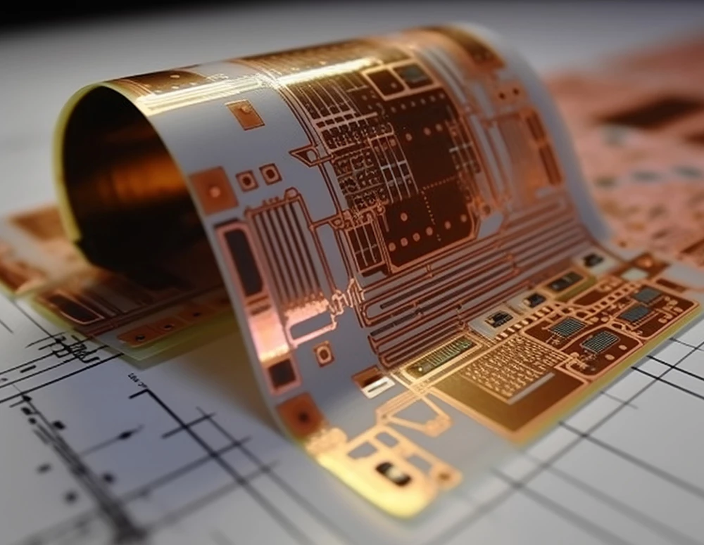
What Makes It Structurally Different
The substrate is polyimide film, not glass-fiber epoxy. Polyimide has a low Young’s modulus — it deforms elastically under bending rather than cracking. The copper on a flex circuit must do the same. That is why copper treatment — rolled annealed versus electrodeposited — matters more to service life than copper thickness. Coverlay replaces liquid solder mask for the same reason: polyimide film bends with the circuit, while solder mask cracks at the first bend.
The fabrication sequence is also different from rigid boards. Flex PCBs require individual sheet handling, pre-bake cycles to remove moisture absorbed by the hygroscopic polyimide substrate, and dedicated tooling for complex non-rectangular shapes. These are not optional steps. The material demands them — and a supplier who skips or compresses them is cutting corners that will show up as yield problems or field failures.
Why Does Flexible PCB Matter Now?
Flexible PCB has been in production for decades. But the scale and sophistication of current demand is different in kind, not just degree.
The global flexible PCB market reached approximately USD 21.8 billion in 2023 — around 30% of total PCB industry revenue — and is projected to grow to USD 27 billion by 2029 at a compound annual growth rate of 8–9%. Four forces are driving this simultaneously: the expansion of 5G infrastructure, the acceleration of EV development, the growth of wearable health devices, and the emergence of foldable consumer electronics. Each sector places demands on circuit design that rigid boards cannot satisfy at scale.
What This Means for Engineers and Buyers Sourcing from China
The practical consequence of this growth is that flexible PCB manufacturing in Shenzhen has matured significantly. More factories now have dedicated flex lines, laser drilling capability, and engineers who understand IPC-2223 design standards. At the same time, product complexity has increased in lockstep — Class 3 medical wearables, automotive BMS interconnects, and foldable phone hinges are now high-volume, not niche, requirements.
For buyers sourcing from China, the gap between capable and incapable suppliers has widened. Basic volume and surface quality are no longer differentiators. DFM engineering depth, material traceability, and validated assembly process control are now the variables that determine whether a supplier can actually execute your project — or just accept the purchase order.
With that context established, the first technical decision is configuration. Which of the four flex PCB types matches what you are building?
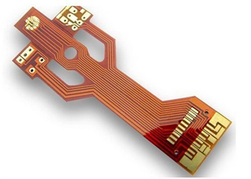
Flexible PCB Types: Which Configuration Fits Your Application?
Choosing the wrong configuration early is expensive. It can force a complete stack-up redesign after tooling has been made — not a file correction, a respin.
The four configurations in current production each have a different cost structure, different mechanical ceiling, and different assembly requirements. The selection is a technical decision based on routing density, bend cycle count, layer count, and total budget — not a preference for simplicity or sophistication.
| Configuration | Layer Count | Best Use Case | Dynamic Flex | Relative Cost |
|---|---|---|---|---|
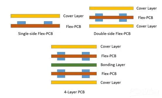
| Single-sided flex | 1 | Ribbon cables, sensor leads, display tails | High | Lowest |
| Double-sided flex | 2 | IoT devices, medical monitors, industrial controls | Moderate — PTHs outside bend zones only | Medium |
| Multilayer flex | 3–8 | Smartphones, cameras, satellites, hearing aids | Low — ≤ 2 flex layers only | High |
| Rigid-flex | 2–10+ | Medical implants, avionics, foldable devices | Selective per zone | Highest |
Single-Sided and Double-Sided Flex
Single-sided flex carries copper on one side of the polyimide film only. It is the most widely used flex configuration in volume production — not because it is a compromise, but because it is the correct solution for a large proportion of real applications. Double-sided flex adds a second copper layer connected through plated through-holes (PTHs). Routing density increases, but so does the constraint: PTHs must stay completely outside every bend zone. PTH barrel walls crack under repeated bending. This is a mechanical failure mode with a predictable outcome, not a guideline to weigh against cost.
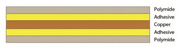
Multilayer and Rigid-Flex
Multilayer flex adds three or more copper layers between flexible dielectric layers. It is specified when routing complexity exceeds what two layers can carry. The mechanical trade-off is direct: each added layer increases total stack thickness, which raises the minimum achievable bend radius. Four-layer and above flex is generally not suitable for dynamic bending applications. Multilayer flex is a routing solution, not a bending solution — and that distinction matters before the design begins.
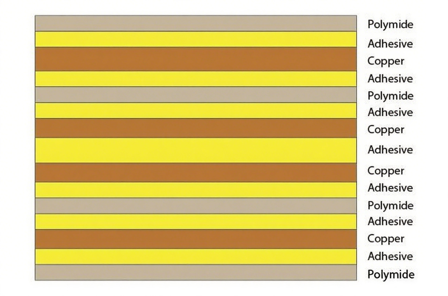
Rigid-flex bonds FR4 rigid zones directly to flex sections within a single board. Components mount on the rigid zones. Flex sections route between them with no board-to-board connectors. The per-board price is the highest of any configuration. Total system cost — once connectors, mating hardware, and assembly labor are removed from the calculation — is frequently the lowest. Rigid-flex is the standard in medical implantables, military electronics, and aerospace avionics because reliability over the product lifetime is the design constraint, not unit board price.
With the right configuration selected, the next decision is the most consequential one in the entire project: the materials that make up the stack-up.
Flexible PCB Material: The Foundation of Every Design Decision
Every performance characteristic of a flex circuit — thermal rating, bend cycle life, signal integrity, and IPC class eligibility — is set by material decisions made before a single trace is routed. Most engineers write “polyimide” in the spec and assume the rest is handled by the factory. That covers roughly 10% of the material decision. The remaining 90% — laminate construction and copper treatment — determines whether the board survives its application.
Three material decisions matter most: substrate type, laminate construction, and copper treatment.
Substrate: Polyimide Is the Standard — Understand Why
Polyimide (PI) is the correct substrate for any flex PCB application involving reflow soldering, elevated operating temperatures, Class 2 or Class 3 IPC requirements, or more than a few hundred bend cycles. The properties that matter in practice:
- Thermal stability: Decomposition temperature above 500°C — compatible with standard lead-free reflow profiles
- Low CTE: Dimensional stability under thermal cycling protects solder joint integrity over the product lifetime
- Dielectric consistency: Stable Dk values across frequency ranges support controlled impedance routing for RF and high-speed digital signals
- Chemical resistance: Resists solvents, acids, and cleaning agents used throughout fabrication and assembly
- FDA biocompatibility: Approved for direct skin contact — a baseline requirement in medical wearable design
PET (polyester) costs less and is appropriate for disposable biosensors, single-use test strips, and low-temperature promotional electronics. Outside that narrow category, PET is the wrong material. Failures do not appear in prototype testing — they appear after the product is in service.
Adhesive vs. Adhesiveless Laminates
Standard flex laminates bond copper to the PI film with an epoxy or acrylic adhesive layer. Adhesiveless laminates deposit copper directly onto the PI film, eliminating that intermediate layer. The performance difference is more significant than it appears on a datasheet:
| Property | Adhesive Laminate | Adhesiveless Laminate |
|---|---|---|
| Cost | Lower | ~20–40% premium |
| Layer thickness | Greater | Thinner — tighter achievable bend radii |
| Dimensional tolerance | ±0.20 mm | ±0.10 mm |
| High-frequency performance | Moderate | Better — no adhesive dielectric variation |
| IPC Class 3 eligibility | Class 1–2 only | Required for Class 3 |
For Class 1 or Class 2 applications, adhesive laminates are cost-appropriate and fully capable. For Class 3 — medical devices, aerospace, defense — adhesiveless is not an upgrade option. It is the required baseline.
Laminate construction defines how the layers bond together. But what those layers are made of — specifically the copper itself — is an equally important decision, and one that most engineers leave unresolved until a failure forces the conversation.
Rolled Annealed vs. Electrodeposited Copper: The Decision Most Engineers Defer
This is where the most undiagnosed flex PCB field failures originate. It is also the material variable most frequently left to manufacturer default.
Electrodeposited (ED) copper is plated onto a carrier drum. Its grain structure runs perpendicular to the foil surface — columnar and brittle under cyclic bending stress.
Rolled annealed (RA) copper is mechanically rolled and heat-treated. Its grain structure runs parallel to the foil surface — layered and ductile. Under repeated bending, RA copper distributes strain across many grain boundaries rather than concentrating it at a few weak points.
The rule is direct: any flex zone that bends more than 100 times over the product’s lifetime requires rolled annealed copper. ED copper is acceptable only for static flex — bend once during installation, fixed for the product’s life. Using ED copper in a dynamic application is a design defect that passes prototype validation and fractures in the field between 30,000 and 80,000 cycles — inside the warranty window, after the product has shipped at volume.
With all three material decisions made, the design layout can begin. The next section covers the rules that govern what can and cannot exist inside a bend zone — and why violating them produces failures that prototype testing will not catch.
Flexible PCB Design Rules: What Your Layout Must Get Right
Design errors cause approximately 78% of flex PCB field failures — not manufacturing defects. The same mistakes appear in the same locations on every failed board, and they share a common origin: bend zones where the physics of repeated bending were not respected during layout.
The core discipline of flex PCB design is stress management. Every trace, via, and component placement either distributes mechanical stress across the structure or concentrates it at a point. Concentrated stress causes fatigue cracking — not during prototyping, but after the product has accumulated cycles in the field.
Flex PCB design is governed by five categories of rules: bend zone classification, minimum bend radius, trace routing geometry, restricted features, and surface protection. Miss any one of them, and the failure will not appear during prototyping — it will appear in the field. The following sections cover each category in the order your layout process should address them.
Static vs. Dynamic: Classify Every Bend Zone Before You Route Anything
Before placing a single trace, classify every bend zone in your design as static or dynamic. This classification changes the minimum bend radius, copper type requirement, via placement strategy, and layer count ceiling for that zone.
Static flex (bend-to-install): Fewer than 100 lifetime bends. The board is bent during assembly and stays fixed for the product’s life. Examples: fixed-equipment panel interconnects, hinged enclosure ribbons, cable replacements.
Dynamic flex (continuous operation): More than 100 bends during the product’s operating life — often exceeding 100,000 cycles. Examples: foldable phone hinges, wearable sensor interconnects, robotic arm wiring, printer head cables.
A single board can have both static and dynamic zones. Each must be classified and managed independently. Applying static rules to a dynamic zone is a guaranteed late failure.
With every bend zone classified, the next step is translating that classification into a specific dimensional constraint — the minimum bend radius the design must meet throughout each flex region.
Minimum Bend Radius Per IPC-2223
IPC-2223 is the governing design standard for flexible and rigid-flex PCBs. Its minimum bend radii are pass/fail thresholds under controlled laboratory conditions — not design safety margins. Always design with at least 20% clearance above the IPC minimums. Real products see temperature variation, humidity, assembly tolerance accumulation, and cumulative fatigue that lab testing does not replicate.
| Layer Count | Approx. Stack Thickness | Static Min. Radius | Dynamic Min. Radius |
|---|---|---|---|
| 1 layer | ~0.15 mm | 1.5 mm (10× thickness) | 15 mm (100× thickness) |
| 2 layers | ~0.25 mm | 2.5 mm | 37.5 mm |
| 4+ layers | ~0.50 mm | 10 mm | Not recommended |
Meeting the minimum radius is necessary, but it is not sufficient. Inside that bend zone, how traces are oriented and routed determines whether the copper survives its cycle count — or fractures long before it should.
Trace Routing Inside Bend Zones
All traces in a bend zone must run perpendicular to the bend axis. Traces running parallel experience direct tensile and compressive loading with every cycle. Fatigue failure rates for parallel-routed traces in dynamic applications run approximately three times higher than for perpendicularly oriented traces.
Beyond orientation, apply these rules consistently across every bend zone:
- Use smooth arcs for all direction changes — not 45° chamfers, and never 90° corners
- Remove copper fills and pours from bend zones — they raise local stiffness and shift the neutral mechanical plane
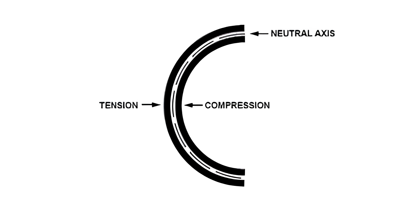
- Position all signal traces at the neutral plane of the stack-up — the layer experiencing neither tension nor compression
- Where current capacity permits, slightly reduce trace width within the bend zone to preserve cross-sectional flexibility
Beyond trace orientation, certain design features must be kept out of bend zones entirely. No amount of correct trace geometry can compensate for a via or through-hole positioned where bending stress will find it.
Features That Must Never Appear Inside a Bend Zone
| Feature | Permitted? | Consequence |
|---|---|---|
| Plated through-holes (PTH) | Never | Barrel walls crack under cyclic bending |
| Surface-mount components | Never | Create local rigidity; stress concentrates at component edges |
| Via-in-pad | Never | Cannot be reliably resin-plugged on flex; solder wicks into via |
| Standard vias | Avoid | Relocate to stiffened or rigid areas |
| 90° trace angles | Never | Stress concentration at corner causes fatigue cracking |
| Copper fills / pours | Avoid | Raise local stiffness; displace the neutral plane |
With prohibited features relocated, the final design layer decision is surface protection and mechanical support — coverlay specification and stiffener placement. Both must be defined in the fabrication files, not communicated verbally.
Coverlay, Solder Mask, and Stiffeners
Coverlay — a polyimide film laminated with adhesive over the copper traces — is the correct surface protection for all flex regions. Liquid photoimageable (LPI) solder mask cracks under bending. LPI is acceptable only in the rigid zones of a rigid-flex board, or in proven static areas. Do not use it on any dynamic flex region.
Stiffeners are FR4 or stainless steel plates bonded to the underside of the flex circuit in connector areas and SMD component zones. Use FR4 for standard SMD zones and ZIF connector areas. Use stainless steel where mechanical load is high or repeated mating is expected.
Define stiffener zones on a dedicated mechanical Gerber layer. Specify material, thickness, and bond method — pressure-sensitive adhesive or thermally cured epoxy. Silkscreen notations do not transfer reliably through a manufacturing workflow. If it is not in the files, it will not be built consistently into the product.
Design rules are locked. Before routing is finalized, surface finish must be selected — because that choice affects both assembly yield and long-term mechanical reliability in flex-specific ways.
Flexible PCB Surface Finishes: A Decision With Assembly Consequences
Surface finish for flex PCBs carries more consequence than for rigid boards. The mechanical demands of flex applications create finish-specific failure modes. The wrong finish in a dynamic bending application does not fail during assembly — it fails in service, after the product has shipped.
Three surface finishes are relevant for flexible PCB applications: ENIG, OSP, and immersion silver.
ENIG: High Performance, With a Dynamic Flex Caveat
ENIG provides a nickel barrier layer and immersion gold surface that deliver low contact resistance — typically under 50 mΩ — excellent corrosion resistance, and compatibility with multiple reflow cycles. It is the standard choice for RF connector pads, fine-pitch SMD components, and any application requiring long shelf life.
The limitation in dynamic flex: the nickel layer introduces stiffness and brittleness at the copper-nickel interface. In tightly wound, high-cycle dynamic applications, micro-cracking at this interface is possible. Specify ENIG where the circuit is predominantly static or low-cycle dynamic, and where ENIG-finished traces do not pass through the most demanding bend zones.
OSP: The Right Call for High-Cycle Dynamic Flex
OSP is an ultra-thin organic coating — under 1 micron — applied to bare copper pads. It costs 50–70% less than ENIG. More importantly for dynamic flex, it adds no rigidity to the copper surface. For wearable electronics, foldable device circuits, and any flex PCB that bends continuously in service, OSP is frequently the technically correct choice — not just the economical one.
The constraint is shelf life. The organic film degrades with humidity and repeated thermal exposure. OSP-finished boards require controlled storage and should be assembled within the manufacturer’s specified window. Multiple reflow cycles or extended pre-assembly storage raise solderability risk.
Immersion Silver: The Dynamic Flex Alternative
Immersion silver provides excellent pad flatness for fine-pitch placement, better shelf life than OSP, and avoids the nickel rigidity concerns of ENIG. It is the right choice when dynamic flex performance and corrosion resistance both matter. The limitation is susceptibility to sulfide tarnishing in high-sulfur environments without sealed packaging.
| Surface Finish | Cost | Flex Compatibility | Shelf Life | Best For |
|---|---|---|---|---|
| ENIG | High | Good (static / low-cycle flex) | Excellent | Medical, RF, precision SMD, multi-reflow |
| OSP | Low | Excellent (high-cycle dynamic flex) | Limited — controlled storage required | Wearables, foldables, high-volume consumer |
| Immersion Silver | Medium | Very good (dynamic flex with corrosion concern) | Good — 12+ months sealed | Dynamic flex with environmental exposure |
| HASL (lead-free) | Low | Poor — uneven surface, thermal stress risk | Good | Not recommended for flex PCB |
With every specification now defined, the complete picture of what happens in the factory can be understood — and where flexible PCB manufacturing cost actually accumulates.
Flexible PCB Manufacturing: What Happens in the Factory
Understanding the fabrication sequence matters because it explains where cost accumulates, where yield risk concentrates, and what questions to ask when comparing suppliers.
Flexible PCB fabrication follows a defined sequence: material preparation and pre-baking → circuit patterning and etching → drilling and plating → coverlay lamination → surface finish application → electrical testing and final inspection. Each step depends on the one before it. A problem introduced in the first step — moisture retained in the substrate — will not be visible until the final step, by which point the board is fully processed and the cost of the defect is at its maximum. The sections below go through each stage in order.
Material Preparation and Pre-Baking
Polyimide is hygroscopic — it absorbs moisture from the atmosphere readily. Before any fabrication process begins, copper-clad polyimide laminates are baked to remove that moisture. Pre-bake duration runs from 2 to 10 hours depending on layer count and stiffener configuration. Skipping or compressing this step is a primary cause of delamination and coverlay bubbling in downstream processing. A supplier who does not pre-bake before fabrication is not following the process the material requires.
Circuit Patterning and Etching
The circuit layout is transferred to the copper surface through photolithography: photosensitive resist is applied, exposed through precision artwork film under UV light, developed to reveal the circuit pattern, then chemically etched to remove unwanted copper. Fine-line capability is a meaningful differentiator between manufacturers. Experienced flex PCB factories achieve trace and space down to 0.075 mm (3 mil) as standard. Leading-edge processes reach below 0.05 mm for high-density designs.
Drilling, Plating, and Coverlay Lamination
Through-holes and vias are CNC or laser drilled, then electroplated to establish inter-layer electrical continuity. Laser drilling is required for blind vias and microvia designs. After plating, coverlay films are cut to precise dimensions, aligned to the circuit, and laminated under controlled heat and pressure. Coverlay window registration accuracy — typically ±0.15 mm at qualified manufacturers — must be confirmed before finalizing pad geometry, especially for fine-pitch designs. Misaligned coverlay windows that encroach on pads cause soldering defects at assembly that are difficult to diagnose without knowing the fabrication tolerance.
Surface Finish Application, Electrical Testing, and Final Inspection
Surface finish is applied after coverlay lamination. For ENIG, the process involves palladium activation, electroless nickel deposition, and immersion gold — each step requiring precise chemistry control to avoid black pad defects (nickel corrosion beneath the gold layer) that destroy solderability invisibly. Per IPC-6013 and IPC-9257, all flex PCBs undergo electrical continuity and isolation testing before shipment. Advanced protocols include flying probe testing for prototypes and low-volume orders, bed-of-nails fixture testing for production runs, HiPot dielectric withstanding voltage testing, and peel strength testing to validate copper-to-substrate adhesion. Boards that fail these tests at the factory do not reach the customer — but boards from factories without these controls do.
Manufacturing quality defines what arrives at the assembly line. Assembly is where most flex PCB projects underestimate the complexity that follows — and where process gaps in the supply chain become visible for the first time.
Flexible PCB Assembly: Where Most Projects Underestimate Complexity
Flex PCB assembly is not standard SMT on a different board shape. The substrate behaves differently under heat. The board cannot support itself on a conveyor. Component placement requires different equipment settings. Each difference has a direct consequence for yield and long-term reliability that not every PCBA shop is equipped to manage.
Pre-Bake and Incoming Inspection
Unlike the pre-bake in fabrication — which removes moisture before processing the raw laminate — the pre-bake at assembly removes moisture that the finished flex PCB has absorbed during shipping and storage. Polyimide continues to absorb moisture after fabrication. If that moisture is not driven out before reflow, it vaporizes during soldering and causes delamination between the coverlay and substrate — a defect called popcorning that destroys the board. Pre-bake before assembly is not optional. It is a process step that must be scheduled into the production plan.
Incoming inspection simultaneously checks coverlay registration, surface finish condition, dimensional conformance, and component moisture sensitivity levels. Fabrication defects that enter the assembly process undetected become assembly defects — and eventually field failures with no clear cause.
Carrier Jigs, Stencil Printing, and Pick-and-Place
Flex PCBs require custom carrier jigs — typically aluminum or thick FR4 — to hold them flat and dimensionally stable during solder paste printing and component placement. Stencil alignment references the carrier, not the flex circuit edge, because flex material does not hold the dimensional precision of rigid FR4 under production conditions. Stencil thickness for flex paste printing typically runs 0.10–0.12 mm — thinner than standard rigid board stencils. Paste volume control is critical: overfilling pads causes bridging; underfilling leaves mechanically weak solder joints that fail early.
Automated placement machines require recalibration for flex carriers. Z-height must be set precisely to avoid nozzle force on the compliant substrate. Fine-pitch BGA, QFN, and 0201 components on flex circuits require placement accuracy of ±0.025 mm or better — a specification not all assembly shops can reliably achieve on flex substrates.
Reflow Profile Management
This is where the most assembly damage occurs in flex PCB production. Flex circuits have lower thermal mass than rigid boards, and polyimide transmits heat differently than FR4. A standard rigid-board reflow profile applied to a flex assembly produces delamination, substrate warpage out of the carrier, and solder joint stress cracking.
Correct flex reflow profiles use slower ramp rates of 1–2°C per second, extended soak zones for thermal uniformity, and controlled cooling. For lead-free processes, peak temperature at the board surface should hold at 245–255°C for 20–30 seconds, never exceeding 260°C at the component body. Rigid-flex assembly adds one further variable: the rigid and flex sections have different coefficients of thermal expansion. During reflow, they expand at different rates, generating stress at the transition zones. Managing this requires zone-specific heating profiles and engineers who have qualified the process on the actual stack-up — not estimated it from general experience.
Post-Assembly Inspection and Testing
After reflow, flex assemblies undergo AOI to detect solder defects, component misalignment, and missing parts. Because flex circuits take a three-dimensional form after assembly, some AOI systems require dedicated flattening fixtures or 3D inspection capability for accurate results. For Class 3 applications, IPC-A-610 Class 3 workmanship standards apply, including solder joint cross-section analysis to verify fill height, void content, and intermetallic layer integrity. Functional testing — applying operating voltages and signals to verify actual circuit performance — should be the final gate before shipment.
With design, materials, surface finish, fabrication, and assembly all understood, the complete cost model can now be built accurately.
Flexible PCB Cost: What You Are Actually Paying For
Flexible PCB manufacturing cost is higher than equivalent rigid PCB cost. The comparison that matters is system cost — not board cost alone. The connectors, wire harnesses, assembly hardware, and warranty exposure that flex circuits replace must be included. When they are, the economics frequently look different from the raw board price.
Primary Cost Drivers
Substrate and laminate specification is the largest single cost variable. Adhesiveless polyimide with rolled annealed copper and ENIG finish on a four-layer stack costs multiples more than adhesive PI with ED copper and OSP on a single layer. The specification must match the application — neither choice is wrong in its correct context, but the decision must be made deliberately.
Layer count and via complexity scale cost directly. Each added layer compounds material, process time, registration risk, and yield pressure. Blind and buried vias add laser drilling and sequential lamination steps that raise per-unit cost significantly beyond through-board PTHs.
Panel utilization affects cost because flex material is processed in fixed panel sizes. Irregularly shaped designs with poor utilization raise effective cost per board. A manufacturer’s engineering team reviewing panel layout during DFM can reduce this significantly.
Order volume is the most impactful per-unit cost variable. Prototypes of a 6-layer flex PCB from Shenzhen typically run USD 80–150 for 5 pieces. Volume production pricing can reduce per-unit cost by 60–80% at scale. Flex PCB economics are highly volume-sensitive because setup and tooling costs amortize across the order.
Lead time directly affects price. Standard Shenzhen production runs 5–7 working days for prototype volumes. Expedited 24–72 hour turnarounds carry a premium. China’s domestic material supply chains, automated production lines, and established logistics infrastructure give Shenzhen manufacturers a structural cost advantage on standard lead times that is difficult to match elsewhere at equivalent quality.
Where Legitimate Cost Savings Are
| Lever | Why It Works |
|---|---|
| Reduce layer count through better routing | Each removed layer has compounding savings on material, drilling, plating, and yield |
| Use standard bend radii | Non-standard radii may require custom forming tooling; standard radii reuse existing tooling |
| Maximize panel utilization | Boards sized to standard panels reduce effective material cost per unit |
| Match surface finish to actual requirements | Defaulting to ENIG where OSP is sufficient adds avoidable cost without performance benefit |
| Share NPI panels | Shared-panel prototyping at many Shenzhen factories significantly cuts prototype unit cost |
With cost understood, the final step before file submission is confirming that every specification decision is locked and documented. Unresolved decisions at the time files are submitted are the primary cause of production delays and DFM hold notifications.
What to Decide Before You Send Your Files
When your Gerber files arrive at a manufacturer’s engineering desk, the DFM review begins immediately. Every ambiguity generates a hold. The seven decisions below are the ones IWDF Solutions’ engineers ask about most frequently — resolving them before submission eliminates the most common delay sources.
1. Is each bend zone classified as static or dynamic?
Include a dedicated Gerber layer marking all bend zones and their classification. Without this, DFM cannot verify bend radius compliance or copper type suitability.
2. What IPC performance class does your application require?
State Class 1, 2, or 3 explicitly in your fabrication notes. Class 3 requires adhesiveless laminates, rolled annealed copper, tighter tolerances, and more rigorous testing. Misspecifying this in either direction has direct cost and reliability consequences.
3. What substrate and copper type are specified?
Specify PI film grade and thickness, copper weight (0.5 oz, 1 oz, 2 oz), copper type (ED or RA), and laminate construction (adhesive or adhesiveless). Do not leave any of these as manufacturer defaults.
4. Are stiffener zones on a dedicated mechanical Gerber layer?
Specify stiffener material, thickness, and bond method. Silkscreen notations do not transfer reliably through a manufacturing workflow.
5. What surface finish does your assembly process require?
If you are handling assembly yourself, confirm that your paste, reflow process, and storage conditions match the specified finish. If IWDF Solutions is managing full PCBA turnkey, our assembly engineers advise on finish selection during quoting.
6. What are your coverlay window tolerances?
Standard registration is ±0.15 mm. Fine-pitch pads may require tighter tolerances. Confirm the manufacturer’s achievable accuracy before finalizing pad geometry.
7. What is your target volume and production scaling timeline?
A 6–12 month forecast lets your manufacturing partner plan material sourcing, panel optimization, and capacity — and gives you an accurate cost model beyond prototype-only pricing.
Flexible PCB Applications: Where These Decisions Have the Most Impact
Understanding how flex PCB design and manufacturing decisions play out across industries clarifies why the details in this article are not optional. They are the difference between a product that qualifies and ships, and one that does not.
Medical Devices and Wearables
Medical flex PCB applications carry the strictest requirements of any sector. Implantable sensors, wearable monitors, surgical instruments, and imaging equipment require Class 3 IPC performance, adhesiveless substrates, ENIG or immersion silver finish, and full material traceability. The polyimide substrate used in wearable sensors has FDA approval for direct skin contact — a requirement that eliminates most alternative substrate materials. Flex circuits allow medical devices to be smaller, lighter, and conformable to anatomical geometry in ways rigid boards cannot replicate.
Automotive and New Energy Vehicles
Automotive flex PCBs must operate from -40°C to +125°C, survive IATF 16949 vibration profiles, and maintain performance across the vehicle’s full service life. The EV transition is a significant driver for flexible PCB manufacturing demand. Battery management system flex circuits monitor and balance individual cells across large, curved battery arrays — a routing challenge that rigid boards and connectors cannot solve as reliably or as compactly in volume production.
Consumer Electronics and Foldable Devices
Smartphones, tablets, earbuds, and cameras use single-sided and double-sided flex circuits for display interfaces, battery connections, antenna routing, and camera modules at volume. Foldable smartphones represent the most demanding consumer flex application: the central hinge circuit must survive 200,000 or more fold cycles at very tight bend radii. This requires adhesiveless PI with RA copper and typically demands OSP surface finish to avoid micro-cracking at the ENIG nickel layer under extreme dynamic bending.
Aerospace and Defense
Aerospace flex circuits must survive thermal cycling from -55°C to +125°C and beyond, radiation exposure, and shock and vibration per MIL-STD specifications, over service intervals with no maintenance access. Weight reduction from replacing wire harnesses with integrated flex circuits has a direct and calculable fuel cost impact — which is why even marginal weight savings justify the cost premium of flex PCB in this sector.
Industrial Automation and IoT
Robotics joints, sensor arrays, motor control feedback circuits, and industrial IoT interconnects increasingly rely on flex circuits for the mechanical degrees of freedom that rigid boards cannot accommodate. The growing sensor density in smart manufacturing drives demand for compact, vibration-tolerant flex solutions in confined machine geometries where rigid board architectures cannot compete.
Why the Manufacturing Partner You Choose Matters as Much as Your Design
A technically correct flex PCB design submitted to the wrong manufacturer produces the wrong outcome. The gap between a generalist PCB shop and a specialist flexible PCB manufacturer is wider than most buyers expect until they encounter it during DFM review or qualification testing.
The questions that determine whether a supplier can actually deliver your requirements are:
| Evaluation Area | What to Ask |
|---|---|
| Fabrication capability | Minimum trace/space? Laser drill for blind vias? PI film thicknesses stocked? Coverlay registration tolerance guaranteed? |
| Assembly infrastructure | Dedicated flex carrier jigs? Flex-specific reflow profiles — documented and measured, not estimated? |
| Quality certifications | ISO 9001 current? ISO 13485 for medical? IATF 16949 for automotive? RoHS/REACH declarations available? |
| IPC compliance | Does the factory inspect to your specified IPC class? IPC-6013 test coupons and reports available? |
| Engineering engagement | Written DFM feedback before order acceptance, or files processed as submitted? |
| Vertical integration | Fabrication and assembly under one roof? Single accountability point across both processes? |
A manufacturer that processes your files without DFM review is accepting your design risk as a production problem. A manufacturer that reviews files, flags issues, and proposes solutions before order placement is delivering engineering value — and is far more likely to produce a reliable product on the first build.
At IWDF Solutions, engineering review starts at the first inquiry. Whether your project begins with a new flexible PCB design, a reverse-engineered existing circuit, or a requirement to reduce flexible PCB manufacturing cost on a current design, our team of 50+ engineers engages at the technical level complex flex projects require. Our services span flexible PCB design, PCB manufacturing, PCB assembly, functional testing, and prototype-to-volume scaling — from Shenzhen to your address, with a single point of accountability.
Conclusion
A flexible PCB project is defined by decisions made in the first few weeks — not by what happens in manufacturing. Material specification, bend zone classification, IPC class selection, copper type, surface finish, and assembly process planning: none of these can be safely deferred without adding risk, time, and cost.
The engineers who get flex PCB right are the ones who ask the right questions early, document answers clearly, and work with a manufacturing partner who engages technically from day one. If you are evaluating a flexible PCB project and want a technical review from an experienced Shenzhen manufacturing partner, contact IWDF Solutions. We provide DFM consultation, design services, prototype fabrication, volume manufacturing, and full PCBA turnkey — with the engineering depth that complex flex projects require.
Frequently Asked Questions
What is a flexible PCB and how does it work?
A flexible PCB is a circuit built on polyimide film that bends and conforms to three-dimensional geometries. Copper traces are patterned on the film, components are soldered to the surface, and a polyimide coverlay protects the circuit. The completed board can fold, twist, and flex repeatedly without fracturing — making it suitable for applications where rigid boards cannot fit or would fail under mechanical fatigue.
What material is used in flexible PCB manufacturing?
The standard substrate is polyimide (PI) film. Copper is laminated onto the PI film using either adhesive bonding (suitable for Class 1–2 applications) or adhesiveless direct deposition (required for Class 3). Copper foil is either electrodeposited (ED) for static applications or rolled annealed (RA) for dynamic bending applications. PET (polyester) is used only in low-temperature, low-cycle consumer applications.
When should I specify rolled annealed copper instead of electrodeposited copper?
Specify rolled annealed (RA) copper for any flex zone that bends more than 100 times over the product’s lifetime. ED copper is acceptable only for static flex — bend once during installation, then fixed. Using ED copper in a dynamic application is a design defect that passes prototype testing and fractures in the field between 30,000 and 80,000 cycles.
What causes flexible PCBs to fail after the product ships?
Approximately 78% of flex PCB field failures trace back to design errors. The most common are: bend radius violations, ED copper used in dynamic applications, traces routed parallel to the bend axis, PTHs placed inside bend zones, and LPI solder mask applied where coverlay is required. Most pass prototype testing and appear only after the product has accumulated cycles in service.
What does flexible PCB manufacturing cost from a Shenzhen factory?
A prototype run of a 6-layer flex PCB typically costs USD 80–150 for 5 pieces. Volume production reduces per-unit cost by 60–80%. Standard lead time is 5–7 working days; expedited 24–72 hour turnarounds carry a premium. The correct cost comparison includes the connectors, harnesses, and assembly labor the flex circuit replaces — on that basis, flex frequently reduces total system cost.
How do I choose between ENIG and OSP surface finish for my flex PCB?
Use ENIG for corrosion-sensitive applications, multiple reflow cycles, fine-pitch connectors, long shelf life, or RF pads — where the circuit is predominantly static or low-cycle dynamic. Use OSP for high-cycle dynamic flex such as wearables and foldables, where avoiding the rigidity of the nickel layer matters and controlled pre-assembly storage is feasible. Use immersion silver when both dynamic flex performance and corrosion resistance are required.
What should I verify before choosing a flexible PCB manufacturer in China?
Verify minimum achievable trace/space, laser drill capability for blind vias, coverlay registration tolerance, whether dedicated flex carrier jigs exist for assembly, whether flex reflow profiles are documented and validated, and which IPC class the factory inspects to. Ask for written DFM feedback before order placement. A manufacturer that processes files without DFM review is not providing engineering value — they are accepting your design risk as their production problem.

