

Printed Circuit Board Assembly (PCBA) represents the critical bridge between conceptual design and market-ready products. Every electronic device that reaches consumers—from industrial control systems to medical monitors—depends on PCBA as the foundation for performance, reliability, and manufacturing scalability. The PCBA process directly influences your product’s ability to meet performance specifications, survive real-world environmental stress, and achieve cost-effective mass production. Understanding PCBA is no longer optional for engineers, procurement professionals, and project managers; it is essential for making informed decisions that impact project timelines, budgets, and product success. This guide provides the comprehensive knowledge you need to select the right PCBA approach for your specific application and industry requirements.
What Is PCBA?
PCBA is the complete assembly of electronic components onto a printed circuit board, followed by rigorous testing and quality verification to ensure the finished board meets functional and reliability specifications. This definition distinguishes PCBA from its often-confused counterpart—the PCB itself, which is only the substrate onto which components are mounted.
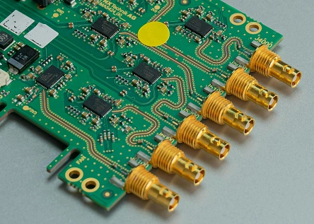
The distinction is fundamental: a PCB is the bare foundation—copper traces etched onto a laminated substrate with drilled holes and finished surfaces. A PCBA takes that foundation and transforms it into a functional, tested, production-ready assembly. The PCBA process encompasses component sourcing, automated and manual soldering, inspection, environmental testing, and packaging.
What PCBA Includes:
- Component sourcing and procurement — sourcing all active and passive components according to your BOM (Bill of Materials), including lead-time management and alternative component selection.
- Surface Mount Technology (SMT) — using automated pick-and-place machines to position and solder thousands of tiny components in seconds.
- Through-Hole Technology (THT) — manual insertion and wave soldering for components requiring mechanical strength or high-current handling.
- Reflow soldering — controlled thermal profiling to achieve consistent, reliable solder joints that meet IPC-A-610 standards.
- Automated Optical Inspection (AOI) — using advanced cameras to detect placement errors, solder bridges, and component misalignment.
- Electrical testing — ICT (In-Circuit Testing) and FCT (Functional Circuit Testing) to verify electrical continuity and functional operation.
- Environmental stress testing — thermal cycling, humidity resistance, and vibration testing for mission-critical applications.
- Traceability and documentation — generating assembly records, test data, and serial tracking for regulatory compliance.
PCBA vs PCB: Why PCBA Is Closer to Your Final Product
Understanding the relationship between PCB and PCBA is crucial for anyone managing electronics projects. While these terms are sometimes used interchangeably in casual conversation, they represent distinctly different stages of product development.

From a decision-making perspective: PCB design addresses the structural and electrical architecture of the board—layer stackup, trace routing, via placement, and impedance control. PCBA selection, by contrast, addresses manufacturability, reliability, cost, and supply chain execution. A beautifully designed PCB can become a problematic PCBA if component selection is poor, assembly processes are inadequate, or testing is insufficient.
From a project management perspective: Engaging a PCBA partner involves coordinating multiple supply chain elements simultaneously—component sourcing across global distributors, managing lead times that vary by market conditions, negotiating component alternatives when original selections become unavailable, and ensuring assembly quality under tightly controlled processes. A PCBA partner must also maintain inventory management, quality documentation, and traceability systems that go far beyond what PCB fabrication alone requires.
The practical consequence is that PCBA decisions made early in your project—component selection, assembly strategy, testing plan—have cascading effects on your ability to ramp production, achieve cost targets, and maintain quality consistency across manufacturing runs.
| Aspect | PCB (Bare Board) | PCBA (Assembled & Tested) |
|---|---|---|
| Scope | Substrate, copper traces, vias, drilled holes | Complete functional assembly with components, solder, testing |
| Primary Focus | Electrical connectivity and board structure | Manufacturability, component integration, functional verification |
| Quality Metrics | IPC-6012 (board specifications) | IPC-A-610 (assembly acceptance criteria) |
| Supply Chain Complexity | Single fabrication partner | Multiple suppliers (components, assembly, testing, logistics) |
| Time to Delivery | 2-4 weeks (fabrication only) | 4-12 weeks (including component sourcing and assembly) |
| Risk Factors | Complete functional assembly with components, solder, and testing | Component obsolescence, supplier availability, assembly yield, testing coverage |
This table illustrates why PCBA partnership is fundamentally more complex than PCB fabrication partnership—and why choosing the right PCBA provider is one of the highest-impact decisions in your product development cycle.
Key PCBA Process Flow: From Files to Functional Boards
The PCBA process follows a well-defined sequence that every electronics professional should understand. Each step represents both an opportunity for quality assurance and a potential risk point that can affect your final product.
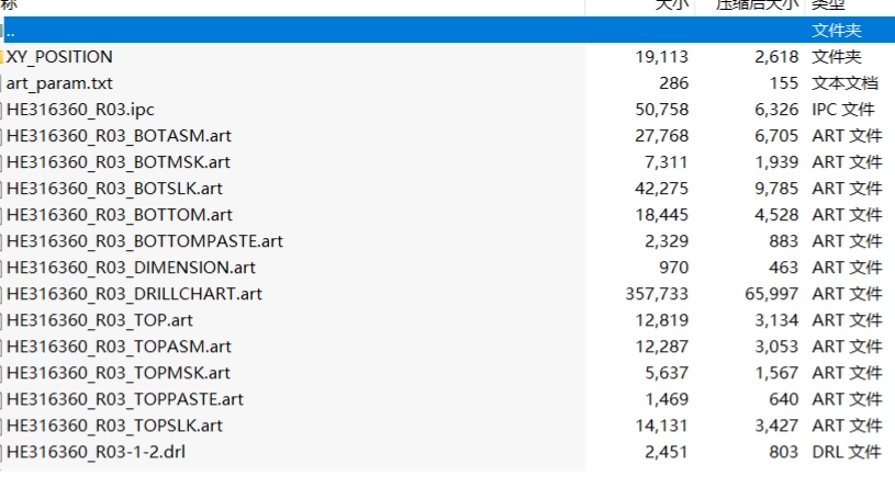
Step 1: DFM/DFA Review and BOM Validation
Before any physical assembly begins, your design files and Bill of Materials enter a critical review phase. DFM (Design for Manufacturability) and DFA (Design for Assembly) analysis examine whether your PCB design is actually feasible within the capabilities of modern manufacturing equipment.
A comprehensive DFM/DFA review identifies issues such as trace widths too narrow for reliable etching, component spacing too tight for pick-and-place accuracy, via placements that interfere with component pads, and thermal relief patterns that may cause assembly failures. This analysis also validates your BOM against current market availability—determining whether specified components are in stock, evaluating lead times, and identifying alternative components if originals become unavailable.
Why this matters to B2B buyers: A manufacturer that skips or minimizes DFM/DFA review will discover problems during assembly, leading to yield loss, schedule delays, and cost overruns. One-stop PCBA partners perform rigorous DFM/DFA before quoting, which prevents expensive surprises during production.

Step 2: Component Sourcing and Lifecycle Management
Component sourcing is far more complex than simply ordering parts from a distributor. A reliable PCBA partner maintains relationships with multiple authorized distributors, monitors component availability across global markets, and anticipates obsolescence issues that could impact your product roadmap.
Component sourcing includes checking lifecycle status (active production, mature, obsolescence notice, or end-of-life), confirming RoHS compliance if required, verifying authenticity against counterfeiting risks, and managing lead times that can range from 2 weeks to 6+ months depending on market conditions. For applications requiring traceability—automotive, medical, aerospace—component sourcing also involves batch tracking and certification documentation.
Why this matters to B2B buyers: Unexpected component unavailability is one of the leading causes of manufacturing delays and cost overruns. Experienced PCBA partners actively manage this risk by maintaining alternative source lists, negotiating strategic component agreements, and communicating proactively when supply disruptions occur.

Step 3: SMT Programming and Stencil Preparation
Before the first component is placed, PCBA facilities program their pick-and-place machines with precise coordinates extracted from your PCB design files. This programming includes component-to-pad alignment, rotation angles, placement speed, and pressure profiles optimized for each unique component type.
Stencil preparation—laser-cutting metal stencils that control solder paste application—requires precision to within ±0.05mm. Stencil design must account for component pad sizes, solder paste volume requirements for different pad geometries, and aperture openings that prevent solder bridges while ensuring sufficient paste for reliable joints.
Why this matters to B2B buyers: Programming errors or stencil design flaws cause widespread assembly defects affecting hundreds or thousands of boards. Manufacturers with rigorous process controls catch these issues before they reach the production line.

Step 4: Reflow Soldering and Wave Soldering
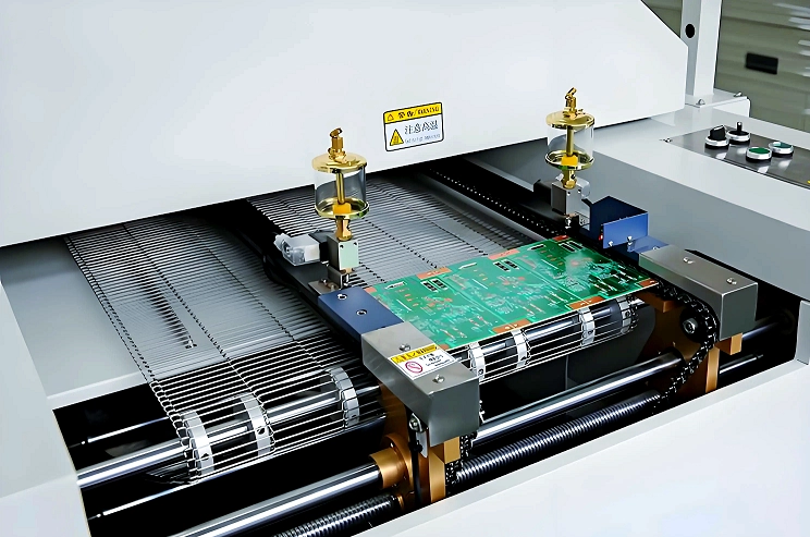
Reflow soldering is the core assembly process for surface-mount components. Solder paste—a mixture of solder powder, flux, and thickening agents—is applied to PCB pads through the stencil. Components are then placed by pick-and-place machines, and the entire assembly is passed through a controlled reflow oven.
The reflow profile is precisely managed: the assembly rises through a pre-heat zone (150-200°C), a thermal soaking zone where flux activates (200-220°C), a reflow peak where solder melts (240-260°C for lead-free solder), and a controlled cool-down zone. Incorrect thermal profiles cause cold solder joints, component damage, and warping.
For through-hole components requiring additional structural strength or high-current connections, wave soldering applies molten solder across component leads in a single pass. This process requires careful board orientation, flux selection, and thermal management to prevent thermal damage to sensitive components.
Why this matters to B2B buyers: Solder joint quality directly impacts product reliability. Manufacturers with advanced thermal profiling, in-process AOI verification, and rework capabilities achieve first-pass yields exceeding 99% for complex assemblies.
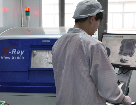
Step 5: AOI, X-ray, ICT/FCT, and Reliability Testing
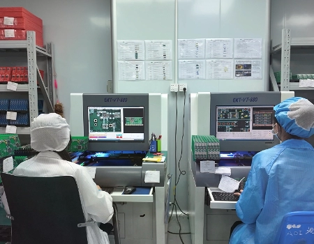
Post-assembly inspection uses multiple verification techniques to detect defects before boards leave the factory:
- Automated Optical Inspection (AOI) examines every solder joint under high-magnification cameras, detecting missing components, incorrect placements, solder bridges, insufficient solder, and component rotation errors.
- X-ray inspection penetrates opaque components like BGAs (Ball Grid Arrays) to verify internal solder ball connections that optical inspection cannot reach.
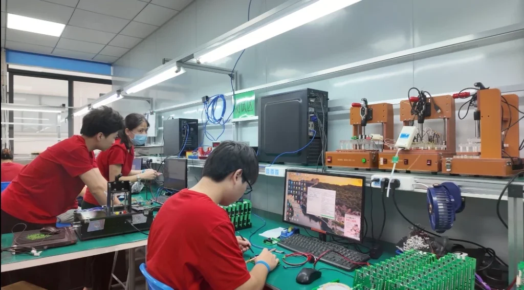
- In-Circuit Testing (ICT) applies electrical signals to probe points, verifying voltage levels, continuity, and component functionality without powering the full board.
- Functional Circuit Testing (FCT) powers the complete assembled board and executes test programs to verify that all functions operate as specified.
For mission-critical applications (automotive, medical, aerospace), additional environmental stress testing includes thermal cycling (-40°C to +125°C repeatedly), humidity/moisture exposure (85°C/85%RH for extended periods), and vibration testing simulating transport and operational conditions.
Why this matters to B2B buyers: Comprehensive testing eliminates defects before they reach your customers. Test coverage typically exceeds 95% for IPC Class 2 assemblies and reaches 100% for IPC Class 3 (high-reliability) assemblies. This investment in testing prevents field failures, warranty claims, and reputation damage.
Step 6: Packaging, Labeling, and Shipment for Mass Production
Final PCBA boards are carefully packaged to prevent electrostatic discharge (ESD) damage and mechanical stress during transit. Professional packaging includes ESD-protective bags, desiccant packets for moisture-sensitive applications, and rigid packaging for assemblies that cannot tolerate flexing.
Labeling includes lot numbers, assembly dates, test records, serial numbers (if required), and certifications (RoHS, lead-free solder, etc.). For large production runs, PCBA partners often maintain kitting services—pre-packaging boards with associated components, accessories, or documentation to accelerate your assembly or distribution processes.
Shipment logistics to your facilities, OEM partners, or distribution centers are managed with full traceability documentation, allowing your quality team to correlate field issues back to specific manufacturing lots and corrective actions.
Why this matters to B2B buyers: A professional PCBA partner treats packaging and logistics as integral to quality assurance, not as an afterthought. This attention to detail ensures boards arrive in perfect condition and documentation is complete for regulatory compliance.
How to Customize PCBA for Your Industry: A Practical Checklist
The ability to customize PCBA is what separates generic contract manufacturers from strategic partners who understand your specific industry requirements. This section provides the practical framework for specifying a custom PCBA that aligns with your application needs.
Define Your Application and Environment
Before contacting a PCBA manufacturer, clearly articulate the environmental and operational context in which your assembly will function. Different industries have radically different PCBA requirements because they operate under different stress conditions.
Consumer Electronics & IoT typically operate in controlled environments (room temperature, standard humidity). PCBA requirements emphasize cost efficiency, rapid time-to-market, and reliability for 3-5 year product lifecycles. Component selection prioritizes commercial-grade parts with standard lead times.
Industrial Automation & Control face temperature extremes (-10°C to +60°C), chemical exposure, electromagnetic interference, and 24/7/365 operation expectations. PCBA requirements include extended operating temperature ranges, conformal coating for chemical resistance, and robust shielding for EMI immunity. Components must be rated for industrial temperature ranges and long-term availability.
Automotive Electronics demand the highest reliability standards. Operating temperature ranges extend to -40°C to +125°C. Thermal cycling (repeated heating/cooling), vibration, moisture intrusion, salt spray exposure, and 10-15 year lifespan expectations mean that every component selection, solder joint specification, and assembly process must comply with AEC-Q200 (components), IPC-6012 Class 3 (PCB), and IPC-A-610 Class 3 (assembly) standards. PCBA partners serving automotive must be AEC-Q101 certified.
Medical Devices require biocompatible component materials, rigorous traceability, FDA or CE Mark compliance pathways, and reliability assurance through accelerated life testing. IPC-A-610 Class 3, IPC-6012 Class 3, and ISO 13485 quality system certification are non-negotiable. Beyond assembly itself, medical PCBA includes specific cleaning requirements (aqueous or no-clean solder residue per IPC standards) and material certifications demonstrating the absence of substances that could react with biological fluids.
Telecommunications & Networking equipment often operates continuously at elevated temperatures (typical ambient + heat generation). Reliability requirements span 7-10 years with minimal maintenance access. PCBA specifications typically require Class 2 or Class 3 assembly, advanced thermal management (thick copper layers, thermal vias), and rigorous environmental stress testing.
Critical guidance: When contacting a PCBA partner with your project, include these environmental parameters: operating temperature range, humidity exposure (sealed vs. exposed), mechanical stress (vibration levels, shock events), chemical exposure (moisture, salt spray, solvent exposure), and expected product lifespan. These specifications drive every PCBA decision downstream.
Prepare Complete Design Data and BOM
A detailed, accurate BOM and complete design file package accelerates PCBA quoting and eliminates costly iterations during production.
Required design files include:
- Gerber files (PCB fabrication data in standard RS-274X format) or ODB++ files (more advanced format containing all design and fabrication information in a single database)
- Drill files (Excellon format) specifying hole locations and sizes
- Pick & Place files (CSV or standard formats) containing X/Y coordinates, rotation angles, and component references
- Assembly drawings showing component placement, reference designators, and critical notes
- Test point documentation identifying which nets/nodes require ICT or FCT probe points

The BOM must specify:
- Component reference designator (R1, C2, U3, etc.)
- Part number (manufacturer part number, not distributor SKU)
- Component description and specification (1K ohm resistor 1/4W, 100uF 16V capacitor, etc.)
- Quantity required
- Preferred supplier or multiple authorized sources
- RoHS compliance status
- Lead-free solder compatibility
- Any special requirements (matched pairs, thermal matched components, etc.)
Critical practice: Specify components that are readily available from multiple global distributors (Digi-Key, Heilind, Wyle Electronics, Arrow Electronics). Avoid single-source components unless necessary, as they create supply chain risk and lead-time uncertainty. When specifying components, confirm that the part number references the correct package size and lead count—many parts have multiple package variants (e.g., 0603 vs. 1206 resistors).
A comprehensive BOM with multiple authorized suppliers and clear specifications reduces PCBA quoting time from weeks to days and prevents costly design revisions during assembly due to component misinterpretation.
Decide on Assembly Strategy: Prototype, Small Batch, Mass Production
PCBA strategies differ significantly across three production phases, and each phase has distinct cost structures, lead times, and quality considerations.
Prototyping (1-10 units) focuses on rapid validation and design verification. Prototyping PCBA typically accepts longer lead times (4-8 weeks including component procurement), higher per-unit costs ($50-500 per board, depending on complexity), and manual quality processes. The objective is not cost optimization but speed-to-market for design verification. Prototyping PCBA is typically produced through “split panels”—multiple different designs assembled on shared PCB panels to distribute fixed setup costs.
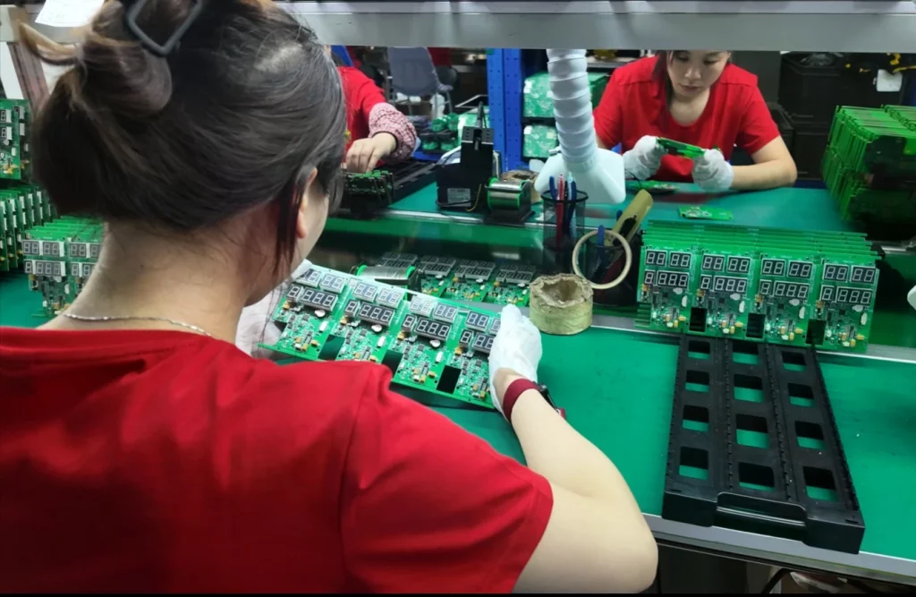
Small Batch Production (10-500 units) represents transition production for small production runs or limited market releases. Small batch PCBA still uses semi-manual processes but begins incorporating automated equipment for efficiency. Lead times compress to 2-4 weeks, per-unit costs drop to $5-50 range depending on complexity, and quality processes begin incorporating AOI and partial functional testing. A small batch is ideal for market entry products, pilot programs, or niche applications.
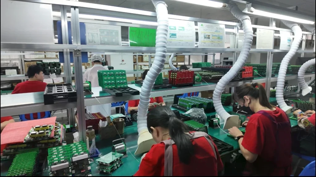
Mass Production (500+ units) optimizes for cost, efficiency, and consistency. Mass production PCBA uses fully automated assembly lines, advanced testing (100% AOI, 100% functional testing), and supply chain optimization through volume purchasing agreements. Lead times stabilize at 1-3 weeks once production ramp begins, per-unit costs drop dramatically ($1-20 for complex assemblies), and quality metrics target 99.5%+ first-pass yield.
The economic implications are significant: producing 100 prototype units costs $5,000-50,000; producing those same boards at mass production scale might cost $500-5,000. However, reaching mass production efficiency requires minimum order quantities that vary by manufacturer and assembly complexity (typically 500-1,000 units minimum).
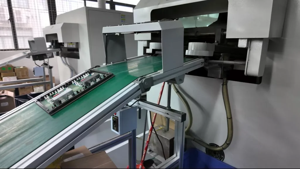
| Parameter | Prototype (1-10 units) | Small Batch (10-500 units) | Mass Production (500+ units) |
|---|---|---|---|
| Lead Time | 4-8 weeks | 2-4 weeks | 1-3 weeks |
| Cost per Unit | $50-500 | $5-50 | $1-20 |
| Setup Costs (NRE) | $1,000-5,000 | $5,000-15,000 | $10,000-50,000 (amortized across volume) |
| Assembly Process | Semi-manual with some automation | Mixed manual/automated | Fully automated assembly line |
| Testing Coverage | Sample-based (20-30% boards) | Partial automated (AOI + sample FCT) | 100% automated (AOI + 100% FCT) |
| Quality Target | First-pass yield 70-85% | First-pass yield 90-95% | First-pass yield 99%+ |
| Typical Application | Design validation, proof-of-concept | Product launch, market entry | Volume production, mature products |
Strategic insight: Plan your PCBA strategy as part of your overall product roadmap. A prototype design might be optimized for rapid iteration and minimum cost, while the same design might be substantially redesigned for mass production to achieve 30-40% cost reduction through component standardization and layer count reduction. Manufacturers offering “design-to-manufacturing” services help bridge this gap by suggesting design modifications in the prototype phase that will dramatically improve mass production economics.
Quality, Testing, and Certification Requirements
Quality standards in PCBA fall into several hierarchical levels, and your application determines which level is appropriate:
IPC-A-610 Class 1 applies to consumer electronics where cosmetic defects are acceptable, and board failures do not create safety concerns. Class 1 assemblies are produced with lower cost processes, less stringent inspection, and baseline testing. This level is appropriate for personal electronics, non-critical IoT devices, and products with short lifecycles where cost is the primary driver.
IPC-A-610 Class 2 applies to industrial equipment, professional-grade electronics, and products where board failure creates economic loss but not safety risk. Class 2 assemblies receive comprehensive AOI inspection, thermal profiling verification, and functional testing of all critical circuits. This level is standard for manufacturing equipment, telecommunications infrastructure, and consumer products with warranty expectations exceeding 3 years.
IPC-A-610 Class 3 applies to mission-critical and safety-critical applications: automotive electronics, medical devices, aerospace/military systems, and critical infrastructure. Class 3 specifies zero defect tolerance for cosmetic and functional issues, 100% visual and automated inspection, 100% functional test coverage, and extensive environmental stress testing (thermal cycling, humidity, vibration, corrosion resistance). Class 3 also mandates full traceability—every component, solder joint, and test result is documented and traceable to specific manufacturing lots.
Beyond IPC standards, your industry may impose additional requirements:
- Medical devices require ISO 13485 quality management system compliance and often FDA 510(k) clearance or CE Mark validation demonstrating safety and effectiveness.
- Automotive electronics require AEC-Q200 component qualification and IATF 16949 manufacturing process certification.
- Aerospace and military require MIL-PRF (Military Performance Specifications) compliance, which specifies component selection, assembly processes, and testing requirements more rigorous than IPC Class 3.
Cost implication: Moving from Class 1 to Class 2 assembly increases PCBA cost by 10-15% due to additional inspection and testing. Upgrading to Class 3 adds another 15-25% due to 100% inspection, extensive testing, and comprehensive documentation. However, this investment is essential for applications where field failures create safety or liability concerns.
Choose the Right PCBA Partner: What to Check
Selecting a PCBA partner is one of the most important supply chain decisions you will make. A poor choice results in quality issues, schedule delays, and cost overruns that cascade throughout your product development cycle. Use this evaluation checklist to assess potential PCBA partners:
- Process Capability and Equipment Capability — Does the manufacturer operate modern SMT lines with specifications matching your board complexity? Can they handle your board size, component density, BGA pitch, and layer count? Do they have through-hole capability if your design requires it? Can they perform specialty processes (HDI, thick copper, high-frequency impedance matching) if your application requires them?
- Testing and Inspection Capability — Do they operate AOI systems? Do they offer X-ray inspection for BGA assemblies? Can they perform ICT and FCT to your specifications? Do they have environmental stress testing capability (thermal chambers, vibration tables, humidity chambers) for reliability validation?
- Quality Certifications — Are they ISO 9001:2015 certified (quality management baseline)? Do they hold IPC-A-610 training certifications for inspection personnel? For automotive applications, are they AEC-Q101 certified? For medical applications, are they ISO 13485 certified? Do they hold UL recognition for PCB materials used in their processes?
- Component Supply Chain Capability — Do they maintain relationships with authorized distributors globally? Can they source components and manage obsolescence issues? Do they proactively communicate when supply disruptions occur? Do they offer alternative component sourcing when preferred parts become unavailable?
- Design Support and NPI (New Product Introduction) Capability — Do they provide DFM/DFA review during quoting? Will they work with your design team to optimize for manufacturability? Can they manage prototyping through to mass production ramp with consistent quality?
- Communication and Project Management — Are they responsive to technical questions? Do they provide regular project status updates? Can they escalate issues quickly if problems occur during production? Do they provide detailed inspection and test reports?
- Traceability and Documentation — Can they provide full genealogy documentation linking components to specific boards and manufacturing dates? Do they maintain long-term records (typically 7-10 years) for regulatory compliance? Can they support root-cause analysis if field issues arise?
- Industry Experience and Case Studies — Have they successfully assembled products in your target industry? Can they reference customers (with confidentiality agreements) who can speak to their capabilities? Do they understand the specific quality and regulatory requirements of your industry?
Practical approach: Request detailed quotes from 2-3 manufacturers for a representative sample of your PCBA design. Compare not only price but also quoted lead times, DFM recommendations (indicating depth of analysis), test coverage proposals, and communication responsiveness. Interview their project managers. The lowest bidder is rarely the best choice—the manufacturer offering the best combination of quality, technical support, and reliability is almost always the superior long-term partner.
Custom PCBA Considerations for Different Industries
Each industry operates under distinct environmental, regulatory, and reliability constraints that shape PCBA customization decisions. Understanding these industry-specific requirements is essential for specifying appropriate PCBA from the outset.
Consumer Electronics & IoT
Consumer electronics prioritize cost, rapid time-to-market, and competitive feature parity. Environmental conditions are typically benign (room temperature, controlled humidity), and product lifecycles are short (2-3 years for rapidly evolving IoT, 3-5 years for mature consumer electronics).
Key PCBA considerations:
- Component selection emphasizes widely available, cost-optimized parts with established supply chains. Single-source components are avoided unless the cost-benefit is substantial.
- Lead-free solder is standard; some legacy products might accept leaded solder, but commercial pressure has largely standardized lead-free processes.
- Packaging and thermal management are minimalist—cost pressure is extremely high.
- Quality target is typically IPC-A-610 Class 1 or borderline Class 2, with 90%+ first-pass yield being acceptable.
- Environmental stress testing is often limited or eliminated entirely, as warranty expectations are typically 1-3 years and failure rates can be absorbed through warranty replacement programs.
When selecting a PCBA partner for consumer electronics:
- Confirm they can meet aggressive cost targets through high-volume automated processes and established supply chain relationships.
- Verify they maintain extensive experience with similar product categories—commodity consumer electronics manufacturers have optimized processes specifically for this market segment.
- Understand their component sourcing capability, as lead-time management is critical for competitive launch windows.
Industrial Automation & Control
Industrial equipment operates continuously in harsh environments (temperature extremes from -10°C to +60°C, vibration, electromagnetic noise, dust exposure) and demands exceptional reliability over 10-15 year product lifespans.
Key PCBA considerations:
- Temperature range expansion requires component selection from industrial-grade suppliers (typically operating -40°C to +85°C minimum). Component costs are 2-3x higher than commercial equivalents.
- Conformal coating (silicone, urethane, or acrylic polymers) is often applied post-assembly to protect against moisture and chemical exposure, adding 5-10% to PCBA cost.
- EMI/EMC considerations require controlled impedance traces, shielded components, and ferrite shielding on critical signals to meet regulatory requirements in industrial environments.
- Thick copper layers (2-3 oz copper) are common to manage high currents and improve heat dissipation.
- Quality target is typically IPC-A-610 Class 2, with environmental stress testing (thermal cycling, humidity cycling, vibration testing) required for critical products.
When selecting a PCBA partner for industrial equipment:
- Confirm they have extensive experience with industrial-grade component suppliers and can manage temperature-rated component sourcing.
- Verify they offer conformal coating capability and have expertise in coating material selection for your specific chemical exposure concerns.
- Confirm their environmental testing capability matches your reliability requirements.
Automotive Electronics
Automotive PCBAs operate under the most demanding conditions in mainstream manufacturing: -40°C to +125°C temperature ranges, thermal cycling stresses (heating/cooling cycles reaching thousands over the vehicle lifespan), vibration exposure, moisture intrusion risk, corrosion potential in salt-spray coastal environments, and 10-15 year reliability expectations without maintenance access.
Key PCBA considerations:
- IPC-A-610 Class 3 assembly is non-negotiable; automotive manufacturers also expect AEC-Q200 component qualification and IATF 16949 process certification.
- Component selection is restricted to AEC-Q200 qualified parts with extended temperature ratings. Automotive-grade components are significantly more expensive than commercial equivalents—often 3-5x the cost.
- 100% component traceability is required—every component tracked from procurement through assembly, enabling root-cause analysis if field issues arise.
- Accelerated life testing is typically required: thermal cycling (-40°C to +125°C repeated 50+ times), moisture resistance testing (IPC-TM-650 moisture absorption/desorption cycles), vibration testing per automotive specifications (MIL-STD-810 or equivalent), and salt spray testing for corrosion resistance.
- Plating specifications are often restricted to immersion silver or ENIG (Electroless Nickel Immersion Gold) rather than cheaper HASL (Hot Air Solder Leveling) to minimize corrosion risk.
- RoHS and REACH compliance is mandatory.
When selecting a PCBA partner for automotive applications:
- Absolutely confirm AEC-Q101 certification and IATF 16949 manufacturing certification—negotiable for any automotive supplier.
- Verify they maintain relationships with automotive-qualified component suppliers and understand component lifecycle management in the automotive supply chain.
- Confirm their environmental testing capability specifically includes automotive-relevant stress profiles (thermal cycling to -40/+125°C extremes, humidity cycling per IPC standards, mechanical vibration per military specifications).
- Understand their PPAP (Production Part Approval Process) capability—automotive OEMs require PPAP documentation for every production run, including FAI (First Article Inspection) reports.
Medical Devices (Non-Implantable)
Medical device PCBA must support patient safety and clinical efficacy. Regulatory pathways (FDA 510(k), CE Mark) impose rigorous quality assurance requirements. Product lifespans extend to 5-10 years, and environmental conditions range from benign (office-based diagnostic equipment) to harsh (patient monitors in ICU environments with thermal extremes, humidity, and chemical exposure from cleaning/disinfection agents).
Key PCBA considerations:
- ISO 13485 quality management system certification is mandatory—this standard specifies design controls, supplier management, traceability, and post-market surveillance requirements.
- IPC-A-610 Class 3 assembly is the baseline; many medical manufacturers require enhanced visual inspection specifications beyond Class 3.
- Material selection must consider biocompatibility—component materials, solder residues, and conformal coating materials must be screened for reactivity with biological fluids and cleaning agents.
- Cleaning requirements are stringent: aqueous cleaning to remove ionic flux residues is typically required (as opposed to no-clean solder processes acceptable in other industries). Post-cleaning processes remove moisture before final packaging.
- Environmental stress testing includes both thermal cycling and moisture absorption/desorption cycles (IPC-TM-650 procedures) to simulate the shelf-life and in-use environment.
- Full traceability extends to lot-level component tracking and long-term retention of manufacturing records (typically 7-10 years minimum).
- Component obsolescence management is critical—medical devices cannot abruptly change component suppliers or introduce design modifications that might affect regulatory clearance.
When selecting a PCBA partner for medical devices:
- Confirm ISO 13485 certification and FDA QSR (Quality System Regulation) compliance knowledge.
- Verify they have experience with medical device PPAP-equivalent documentation (Design History Files, risk management reports, etc.).
- Confirm their understanding of biocompatibility requirements and material screening processes.
- Understand their cleaning process expertise—aqueous cleaning for medical-grade PCBA is distinctly different from consumer electronics processes.
Telecommunications & Networking
Telecommunications equipment operates continuously (24/7/365) in varied environments—from air-conditioned server rooms to field-mounted equipment exposed to temperature extremes and weather. Reliability expectations span 5-7 years with minimal maintenance access, and regulatory requirements often include FCC compliance (electromagnetic emissions/immunity) and sometimes international certifications (CE Mark, etc.).
Key PCBA considerations:
- The temperature operating range typically specifies 0°C to +50°C, but thermal design must account for internal heat generation—component selection often specifies commercial-grade parts rated to +70°C or higher to maintain margin.
- Controlled impedance traces are standard—network equipment operates at high signal speeds (gigahertz frequencies in modern systems) where impedance control is critical for signal integrity.
- Dense component placement is common to minimize board size and cost. BGA (Ball Grid Array) components are prevalent, requiring X-ray inspection to verify internal solder connections.
- EMI shielding and EMC compliance require careful PCB design and component placement to meet FCC Part 15 or equivalent international standards.
- Quality target is typically IPC-A-610 Class 2, with representative environmental testing (thermal cycling, humidity resistance).
When selecting a PCBA partner for telecommunications:
- Confirm their controlled impedance capability and experience with high-speed signal integrity requirements.
- Verify they have expertise with BGA components and X-ray inspection capability.
- Confirm their EMI shielding and grounding design expertise.
Cost Drivers of Custom PCBA and How to Optimize Them
PCBA cost is driven by multiple interconnected factors. Understanding these cost drivers enables you to make strategic decisions that deliver cost reduction without compromising quality or reliability.
Primary Cost Components
PCB substrate cost (15-25% of total PCBA cost) is determined by board area, layer count, material selection, and special processes. A 2-layer PCB is dramatically cheaper than a 10-layer high-density PCB because layer count drives material consumption, fabrication tool hours, and scrap rates. Material selection impacts cost—standard FR-4 (fiberglass-reinforced epoxy) is the cheapest, while high-Tg FR-4 (resisting higher temperatures before delamination), polyimide, and specialty materials cost more. Special processes (blind/buried vias for HDI, thick copper for power applications, controlled impedance traces) add 20-50% to base PCB cost.
Component cost (40-60% of total PCBA cost) is dominated by active components—microprocessors, FPGAs, application-specific ICs—which often account for 80%+ of total component cost. Passive components (resistors, capacitors, inductors) are cheap in isolation but expensive in aggregate when quantities reach tens of thousands per board. Component cost is volatile, driven by supply/demand dynamics, semiconductor manufacturing capacity, and market cycles. During shortage periods, component costs can double or triple.
Assembly labor and machine cost (10-20% of total PCBA cost) depends on assembly complexity, component count, and production volume. SMT machine programming and stencil fabrication are one-time “NRE” (non-recurring engineering) costs that are amortized across production volume. For prototype quantities, NRE dominates cost. For mass production quantities, amortized NRE becomes negligible. Manual assembly steps (through-hole insertion, specialty component placement, conformal coating application) add significantly to labor cost.
Testing and inspection cost (5-10% of total PCBA cost) includes AOI machine time, X-ray inspection for BGAs, in-circuit testing (ICT) probe development and execution time, functional testing software development, and environmental stress testing. Class 3 high-reliability PCBA includes 100% testing coverage; Class 1 consumer PCBA might include only 10-20% sampling inspection.
Packaging, documentation, and logistics (3-7% of total PCBA cost) include ESD-protective packaging, desiccant packets, label design and printing, testing report documentation, and freight to your facilities or downstream assembly partners.
Key Variables That Influence Price
| Variable | Impact | Optimization Strategy |
|---|---|---|
| PCB layer count | 2-layer costs ~$5; 6-layer costs ~$15; 10-layer costs ~$30+ per board for 100-unit volume | Minimize layers through careful routing—eliminate unnecessary layers; consolidate signals onto fewer layers where possible |
| PCB board area | Cost scales roughly with area—doubling board size doubles material cost | Minimize board footprint through aggressive component placement and trace routing; consider form-factor requirements vs. cost |
| Component count | 100 components typically add $50-100 to assembly cost; each additional 100 adds $30-50 more | Consolidate functions into fewer, higher-integration ICs; eliminate redundant filtering/buffering |
| Component sourcing difficulty | Standard, widely available components cost $0.10-1.00 each; specialty/obsolete components cost $5-50+ each | Specify components from multiple authorized distributors; use commercial-grade where reliability allows |
| BGA component count | BGAs add complexity—each BGA requires specialized placement accuracy, X-ray inspection, potential rework | Use BGAs only when justified (high pin density, performance requirements); consider LQFP alternatives for lower pin counts |
| Test coverage requirement | Class 1 testing (sample-based) costs $2-5 per board; Class 3 testing (100% coverage) costs $10-25 per board | Optimize test requirements—specify Class 1 for non-critical assemblies; Class 3 only for mission-critical boards |
| Environmental stress testing | BGAs add complexity—each BGA requires specialized placement accuracy, X-ray inspection, and potential rework | Limit environmental testing to critical designs; use statistical sampling for large production runs (vs. 100% testing) |
| Production volume | NRE costs (programming, stencil, test software) are large for small volumes but negligible for high volumes | Prototype volumes face high per-unit costs due to NRE amortization; commitment to 1,000+ unit volumes drops per-unit cost 50-70% |
Strategic Cost Optimization Approaches
1. Design for Manufacturability (DFM) Review During Prototype Phase
Before committing design to production, conduct a comprehensive DFM analysis identifying cost reduction opportunities. A typical DFM review identifies 20-30% potential cost savings through design modifications that are “free” in the prototype phase but require costly redesign after production commitment.
Example optimizations:
- Reducing PCB layer count from 6 to 4 layers by eliminating unnecessary power/ground planes or consolidating signal routing
- Replacing specialty components with commercial equivalents that meet functional requirements
- Simplifying board geometry to standard rectangular shapes (round or complex shapes add fabrication cost)
- Standardizing component footprints to industry-standard sizes (0402 for resistors, 0603 for capacitors) vs. specialty footprints
2. Component Standardization and Supplier Diversification
Specify components available from multiple authorized distributors with stable, long-term pricing and reliable supply. Avoid single-source components unless the performance advantage is substantial and cannot be achieved through alternatives.
Actively manage component lifecycle—work with suppliers to identify when preferred components are approaching obsolescence and select alternatives early, before supply becomes impossible.
3. Phased Production Strategy: Prototype → Small Batch → Mass Production
Design your prototype phase with an explicit eye toward mass production. Accept slightly higher prototype costs if the design enables lower mass production costs. A design optimized only for prototype cost might cost $20/unit in prototype but $15/unit in mass production; a design optimized for mass production might cost $25/unit in prototype but $5/unit in mass production—the investment is justified by the dramatic ramp benefit.
4. Strategic Batch Sizing
Small batch quantities (100-500 units) offer a good middle ground between prototype costs and mass production costs. Instead of jumping directly from 10-unit prototypes to 5,000-unit production runs, consider 500-unit small batch production to validate design in volume, identify any yield issues, and establish supply chain before committing to full mass production.
5. Collaborative Supplier Partnerships
Establish long-term relationships with PCBA partners who understand your product roadmap and industry requirements. Experienced suppliers proactively identify cost optimization opportunities, manage component sourcing across supply cycle variations, and can apply volume pricing retrospectively as cumulative orders increase.
How to Work with a One-Stop PCBA Partner?
A one-stop PCBA partner manages the complete electronics manufacturing ecosystem—design collaboration, component sourcing, assembly, testing, and logistics—enabling you to reduce supplier complexity, shorten project timelines, and improve quality consistency. Understanding how to work effectively with a one-stop partner maximizes these benefits.
The Value Proposition of One-Stop PCBA Partnership
Supplier consolidation: Instead of managing relationships with PCB fabricators, component distributors, assembly houses, and logistics providers separately, you manage a single PCBA partner relationship. This consolidation reduces communication overhead, eliminates finger-pointing when issues occur, and enables supply chain optimization that isolated vendors cannot achieve.
Project timeline acceleration: Integrated PCBA partners coordinate component sourcing, PCB fabrication, and assembly sequentially—as soon as PCBs arrive, assembly begins; as soon as component shortages are identified, alternatives are sourced without waiting for individual distributor communications. Integrated project management reduces total project duration by 10-20% compared to managing separate vendors.
Quality consistency: A single partner implementing consistent assembly processes, testing protocols, and documentation standards delivers more predictable quality across prototype, small batch, and mass production phases. Supply chain variability is reduced because component sourcing, logistics, and assembly are coordinated by a single entity.
Cost optimization: One-stop partners leverage volume purchasing power with component suppliers, negotiate favorable logistics rates through volume freight arrangements, and amortize equipment investment across a diversified customer base. These advantages translate to 10-20% cost reduction compared to fragmented vendor approaches.
Supply chain resilience: During component shortage periods, integrated PCBA partners actively manage alternative sourcing across their customer base, prioritize supply allocation based on customer strategic importance, and communicate proactively about supply-chain disruptions. Customers working with fragmented vendors often discover supply problems only after production is scheduled to begin.
How IWDF Solutions Manages the Full PCBA Lifecycle
IWDF Solutions, as a representative one-stop PCBA partner, illustrates how integrated PCBA coordination delivers customer value across the full product development cycle.
Phase 1: Initial Evaluation and RFQ Response
When you submit an RFQ (Request for Quote), IWDF’s engineering team conducts a comprehensive DFM/DFA analysis on your design files, identifying potential manufacturability issues and cost optimization opportunities. This analysis includes:
- Detailed review of PCB design for trace spacing compliance, via placement optimization, and layer utilization efficiency
- BOM component verification—confirming all parts are in current production status, checking current availability/lead times, and identifying alternative suppliers
- Assembly process capability assessment—confirming that component placement density is achievable with IWDF’s equipment, identifying any specialty assembly requirements
- Testing capability verification—confirming that your specified test coverage is achievable within the quoted price
- Cost estimation with transparent breakdowns showing PCB cost, component cost, assembly cost, testing cost, and packaging cost
This comprehensive analysis typically requires 3-5 business days, but prevents surprises during production. The quote IWDF provides includes specific recommendations for design modifications that reduce cost while maintaining performance—recommendations that would cost significantly more to implement after production begins.
Phase 2: Design Optimization and Prototype Planning
For projects proceeding to the prototype phase, IWDF works collaboratively with your design team:
- Component sourcing begins immediately—IWDF’s procurement team identifies current market availability, negotiates lead times with distributors, and flags any components approaching obsolescence
- PCB fabrication is coordinated to align with component availability—if critical components have 8-week lead times, PCB fabrication is scheduled to complete just before component arrival, minimizing the time components sit in inventory
- Assembly scheduling is planned to maximize machine utilization and meet your target prototype availability date
- Test program development begins—ICT test probe placement is finalized, functional test software is written to your specifications, environmental test protocols are confirmed
By prototype phase completion, IWDF provides:
- Full prototype PCBA assemblies, tested to your specifications
- Detailed test reports documenting yield, defect analysis, and any rework performed
- Design observations documenting any manufacturing issues encountered and recommendations for design modification in production phase
- Component sourcing and lead-time analysis for production phase planning
Phase 3: Production Ramp Preparation
Between prototype and small batch/mass production phases, IWDF prepares for volume production:
- Supply chain optimization: component purchasing agreements are established with distributors to secure volume pricing and allocation priority; long-lead-time components are purchased early to prevent supply-induced schedule delays
- Production readiness: SMT machine programming is refined based on prototype assembly experience; pick-and-place placement accuracy is verified; solder reflow oven thermal profiles are validated
- Stencil and fixture design: if production volume justifies custom stencils or test fixtures, these are designed and fabricated before production begins
- Quality plan finalization: test coverage, inspection protocols, and documentation procedures are locked in; training is provided to production floor personnel
Phase 4: Small Batch and Mass Production Execution
Once small batch production begins, IWDF provides:
- Weekly or bi-weekly production status reports, including completion status, yield rates, any quality issues encountered, and schedule forecasts
- Daily quality metrics: first-pass yield, defect analysis, rework rates, and test data
- Proactive communication if issues arise (component availability changes, quality anomalies, schedule risks)
- Full traceability documentation linking components to specific manufactured lots, enabling root-cause analysis if field issues arise
- Regular business reviews with your team to discuss yield trends, identify continuous improvement opportunities, and plan for future product variants
Phase 5: Scaling and Continuous Improvement
For successful products, IWDF helps optimize production economics as volumes scale:
- Progressive design refinement: as manufacturing experience accumulates, design modifications are identified that reduce cost without compromising performance
- Supplier relationship management: as volumes increase, IWDF renegotiates component pricing with distributors, securing volume discounts that are passed to you
- Process optimization: manufacturing data is analyzed to identify efficiency improvements; operator training is refined based on yield analysis
- Supply chain diversification: alternative suppliers are qualified for critical components, enabling supply chain resilience and volume pricing negotiation leverage
Industry Capabilities and Quality System Infrastructure
IWDF Solutions maintains comprehensive industry certifications and process capabilities:
Quality system certifications:
- ISO 9001:2015 (general quality management)
- IPC-A-610 training certification (assembly quality standards)
- AEC-Q101 certification (automotive supplier qualification)
- ISO 13485 certification (medical device quality management)
Assembly process capabilities:
- SMT assembly with equipment supporting component sizes from 01005 (0.4mm × 0.2mm) to large, odd-shaped components
- Through-hole assembly for components requiring mechanical strength
- BGA (Ball Grid Array) assembly with X-ray inspection capability
- HDI (High-Density Interconnect) assembly with controlled impedance capability
- Thick copper assembly (up to 4 oz copper) for high-current applications
- Fine-pitch assembly (down to 0.4mm pitch BGAs) for high-density designs
Testing infrastructure:
- Automated Optical Inspection (AOI) for 100% solder joint verification
- X-ray inspection for BGA internal solder verification
- In-Circuit Testing (ICT) with probe capability for high-complexity assemblies
- Functional Circuit Testing (FCT) with custom test program development
- Environmental stress testing chambers (thermal cycling, humidity resistance testing)
- Conformal coating application for moisture/chemical protection
Industry experience:
- Consumer electronics (IoT devices, personal electronics, wearables)
- Industrial automation (process control, machine vision, motion control)
- Automotive electronics (control modules, sensor interfaces, power management)
- Medical devices (non-implantable diagnostic and monitoring equipment)
- Telecommunications (network infrastructure, base station equipment)
Intellectual Property Protection
IWDF Solutions recognizes that many customers operate in competitive markets where design confidentiality is essential. IWDF maintains:
- Comprehensive NDA (Non-Disclosure Agreement) policies that remain in force indefinitely
- Restricted access to design files—only personnel directly involved in your project have access to your designs
- Design file encryption and secure storage systems
- No reverse-engineering of customer designs under any circumstances
- No secondary manufacturing or sharing of customer designs with third parties
This IP protection framework enables customers to confidently share proprietary designs and manufacturing requirements without concern that designs will be shared with competitors.
FAQ: Common Questions About Custom PCBA
What information do I need to provide to get an accurate PCBA quote?
Accurate PCBA quotes require complete technical documentation, including:
- (1) Gerber or ODB++ PCB fabrication files in standard format;
- (2) a detailed Bill of Materials specifying manufacturer part numbers, quantities, and preferred suppliers;
- (3) Pick & Place files containing component placement coordinates and rotation angles;
- (4) assembly drawings showing component reference designations and special notes;
- (5) test specifications, including which nets/nodes require testing and the acceptable test coverage level;
- (6) expected production volume and timeline;
- (7) any special requirements like conformal coating, environmental testing, or traceability documentation.
Providing complete documentation enables PCBA partners to conduct a thorough DFM review and provide transparent quotes with accurate cost and lead-time estimates. Incomplete documentation results in “ballpark” quotes that often prove inaccurate during production, forcing scope changes and schedule delays.
How long does a custom PCBA usually take from order to shipment?
PCBA lead times depend on the production phase and component sourcing complexity. Prototype PCBA typically requires 4-8 weeks, including component procurement and assembly—this extended timeline reflects the need to source individual components from multiple distributors and manage small batch assembly processes. Small batch production (10-500 units) typically requires 2-4 weeks for established designs with in-stock components.
Mass production (500+ units) typically requires 1-3 weeks once production begins, but initial setup and production ramp may require an additional 1-2 weeks. However, these timelines assume all components are in current production and available from distributors. If your design includes components with long lead times (8-12 weeks) or components approaching obsolescence, overall project timelines extend accordingly.
Strategic planning—identifying long-lead-time components early in the design phase and working with PCBA partners to source these components proactively—can reduce total project duration by 20-30% compared to reactive approaches.
Can one factory handle both prototype and mass production?
Yes, professional PCBA partners operate with sufficient flexibility to manage prototype quantities through to mass production scale. However, the approach differs significantly across production phases. Prototype PCBA typically uses shared panels and semi-automated processes to achieve cost-effectiveness for small quantities. As volumes increase, production transitions to dedicated assembly lines with optimized processes, resulting in dramatic per-unit cost reduction.
The advantage of selecting a single partner for prototype through mass production is process consistency and supply chain continuity—component sourcing, assembly processes, testing protocols, and quality standards remain stable, enabling predictable scaling and quality consistency.
However, transitioning between production phases often triggers design and process refinements that reduce cost or improve yield in the high-volume environment. Professional partners proactively identify these optimization opportunities during the prototype phase, enabling design modifications that deliver 30-40% cost reduction when transitioning to mass production.
What are the main quality standards I should specify for my application?
Quality standards depend on application criticality and regulatory requirements. For consumer electronics where cost is the primary driver and board failure does not create safety concerns, IPC-A-610 Class 1 is appropriate. For professional and industrial equipment where board failure creates economic loss, IPC-A-610 Class 2 is standard. For automotive, medical, aerospace, and safety-critical applications, IPC-A-610 Class 3 is mandatory.
Beyond IPC standards, your industry may impose additional requirements: automotive applications require AEC-Q200 component qualification and IATF 16949 manufacturing certification; medical applications require ISO 13485 quality system certification and often FDA or CE Mark compliance. Consult your industry regulatory requirements and competitive product specifications to determine the appropriate quality level—over-specifying quality increases cost unnecessarily, while under-specifying creates field reliability risks.
What testing should I specify for my application?
Testing selection depends on application reliability requirements and cost constraints. For consumer electronics, sample-based testing (20-30% of boards) with basic functional verification is typical and cost-effective. For industrial equipment, 100% automated optical inspection plus representative functional testing provides good quality assurance without high cost.
For mission-critical and safety-critical applications (automotive, medical, aerospace), 100% testing coverage, including automated optical inspection, automated X-ray inspection for BGAs, 100% functional circuit testing, and extensive environmental stress testing (thermal cycling, humidity resistance, vibration testing), is appropriate—despite substantial cost, the field failure prevention ROI is justified.
Your PCBA partner should help you balance testing coverage with cost—over-testing increases cost unnecessarily while under-testing creates field reliability risks. A structured risk assessment considering application failure consequences, regulatory requirements, and warranty expectations guides appropriate testing selection.
How to Start Your Custom PCBA Project?
Moving from planning to execution is straightforward with a professional PCBA partner. Here’s how to initiate your custom PCBA project with IWDF Solutions:
Step 1: Gather project documentation — Collect your PCB design files (Gerber or ODB++ format), Bill of Materials with manufacturer part numbers and quantities, assembly drawings, test specifications, and production volume/timeline expectations.
Step 2: Project overview — Provide a brief description of your application (industry, product category, reliability requirements), expected volumes, and target timeline. This enables IWDF to assess whether your project aligns with their capabilities and schedule.
Step 3: Submit complete RFQ package — Provide all technical documentation to IWDF’s engineering team. Within 3-5 business days, IWDF’s team will conduct a comprehensive DFM/DFA analysis, identify cost optimization opportunities, and provide a transparent quote, including a detailed cost breakdown and design recommendations.
Step 4: Schedule engineering consultation — Once you’ve reviewed the quote and DFM recommendations, schedule a call with IWDF’s engineering team. This consultation typically covers: (1) explanation of DFM recommendations and cost optimization opportunities; (2) clarification of testing and quality requirements; (3) component sourcing strategy and lead-time management; and (4) prototype and production phase planning.
Step 5: Commit to the prototype phase — Based on engineering consultation, commit to the prototype phase. IWDF’s team will immediately begin component sourcing, coordinate PCB fabrication with component availability, and develop test programs to your specifications. Your prototype assemblies will be ready within 4-8 weeks, delivered with complete testing documentation and design observations for production optimization.
Step 6: Plan production scaling — Using prototype results and test data, plan your transition to small batch or mass production. IWDF’s team will refine assembly processes, finalize supply chain optimization, and prepare production readiness. Your production PCBA will be cost-optimized, yield-optimized, and ready to scale predictably.
Why partner with IWDF Solutions for custom PCBA:
- One-stop integration: From design support through production scaling, IWDF manages the complete PCBA ecosystem, eliminating supplier coordination complexity and ensuring supply chain consistency.
- Engineering expertise: IWDF’s team includes seasoned manufacturing engineers who proactively identify cost and yield optimization opportunities, not just reactive assembly and testing.
- Industry experience: IWDF has successfully delivered PCBA solutions for consumer electronics, industrial automation, automotive electronics, medical devices, and telecommunications applications, bringing deep industry-specific knowledge to every project.
- Quality commitment: Comprehensive quality certifications (ISO 9001:2015, IPC-A-610, AEC-Q101, ISO 13485) and full process transparency ensure your PCBA meets your reliability and regulatory requirements.
- Intellectual property protection: Comprehensive NDA policies and restricted-access design file management protect your proprietary designs throughout the manufacturing process.
Your next step: Contact IWDF Solutions with your custom PCBA project. Provide your project overview, design files, and production timeline. Within days, IWDF’s engineering team will provide detailed analysis, transparent quoting, and a clear roadmap for moving from concept to production-ready PCBA.

