

Printed Circuit Boards (PCBs) are the backbone of almost every electronic device we use today. While single-layer and double-layer PCBs are common for simpler devices, multilayer PCBs are essential for complex and high-performance electronics such as smartphones, computers, and medical devices. This guide aims to provide an easy-to-understand overview of multilayer PCB design, from the basics to advanced tips and best practices, enabling beginners and professionals alike to create reliable, efficient, and manufacturable multilayer PCBs.
Multilayer PCB design guidelines include proper stack-up configuration, power/ground plane isolation, trace impedance control, and return path optimization. Tips cover layer symmetry, via optimization, fabrication tolerances, and EMC strategies. By adhering to these principles, engineers can achieve reliable signal performance, manufacturability, and thermal stability in complex multilayer designs.
Let’s explore the critical rules and actionable techniques that shape reliable multilayer PCB designs across industries.
Multilayer PCB Design Fundamentals
What is a Multilayer PCB?
A multilayer PCB is a circuit board with more than two copper layers separated by insulating dielectric material. These layers are laminated together under high temperature and pressure, creating a compact, reliable structure. For example:
- 4-layer PCB: Two signal layers with one power plane and one ground plane.
- 8-layer PCB: More complex with multiple signal layers, ideal for high-speed designs.
This structure allows signals to be routed in different planes, reducing interference and improving performance.


Advantages and Application Areas
Multilayer PCBs offer clear advantages:
- High component density: Enables smaller devices with more functionality.
- Improved signal quality: Dedicated ground and power planes reduce noise and provide stable reference points.
- Better EMI control: Controlled stack-ups help minimize electromagnetic interference.
- Thermal management: Heat dissipation can be optimized through plane layers.
- Mechanical strength: Additional layers increase board rigidity.
Applications include:
- Consumer electronics (smartphones, laptops, wearables)
- Automotive electronics (ADAS, infotainment, EV systems)
- Industrial automation (controllers, sensors, IoT)
- Aerospace and defense (radar, avionics, satellite systems)
- Medical devices (imaging equipment, monitoring systems)
For product developers and startups, these benefits translate into smaller, faster, and more reliable products.
1. Stack-Up Planning: The Foundation of Any Multilayer PCB
Every successful multilayer PCB begins with a sound stack-up strategy. It’s not just about counting layers; it’s about functional separation, impedance control, and EMI shielding.
Common Layer Counts and Structures
The number of layers depends on design complexity:
- 4 layers: Most common for mid-complexity boards.
- 6 layers: Adds flexibility for separating power, ground, and high-speed signals.
- 8–12 layers: Used in high-speed computing, networking, or aerospace
Start with clearly defined signal types: high-speed signals, low-speed digital, analog, and power distribution.
For a 6-layer board, for example, a common stack-up is:
L1: Top Layer – Signal
This is the primary component side and signal routing layer.
- Typically used for high-priority signals: clocks, high-speed data lines, differential pairs.
- It sits directly above a ground plane (L2), forming a microstrip structure for controlled impedance.
- Because components are mounted here, this layer often handles short, direct connections from IC pins.
L2: Ground Plane
A solid, continuous ground plane that serves as the return path for signals on L1.
- Ensures low-impedance return paths, reducing loop area and electromagnetic interference (EMI).
- Helps maintain consistent impedance for L1 signals.
- Also acts as a shield to suppress crosstalk between adjacent traces on L1.
L3: Inner Signal Layer
This layer routes secondary signals—either medium-speed signals or those with less timing sensitivity.
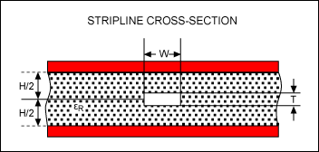
- Sandwiched between two planes (L2 and L4), forming a stripline structure, which provides excellent EMI shielding.
- Often used for differential pairs or delay-matched signals requiring tighter control.
- Less exposed to external noise, making it suitable for analog or sensitive traces.
L4: Power Plane
This is the main power distribution layer, often carrying multiple voltage domains (VCC, 3.3V, 1.2V, etc.).
- Positioned close to L3 and L5 to reduce power distribution impedance.
- Should be a solid copper layer (not split into too many islands) to ensure stable power delivery.
- Works with the adjacent ground plane (L5) to form decoupling capacitance between layers, improving power integrity.
L5: Ground Plane
Another dedicated ground layer, mainly supporting L6 signal routing.
- Creates a stripline environment for L6, just like L2 does for L1.
- Acts as a reference plane for bottom-layer signals and further suppresses EMI from signals on L4 or L6.
- Having two ground planes (L2 and L5) in this stack-up enhances the board’s EMC performance.
L6: Bottom Layer – Signal
The secondary component or routing layer is typically used for low-speed signals or I/O traces.
- Often used for control signals, GPIOs, or less-critical traces.
- Like the top layer, it forms a microstrip structure with its adjacent ground plane (L5).
- May also carry debug/test signals, connectors, or interface lines.

This configuration allows high-speed traces to reference solid planes and maintains symmetry to minimize board warping during fabrication.
Symmetry matters. An asymmetric stack-up can cause mechanical stress during lamination, leading to bow and twist, especially in larger boards.
Also, work closely with your fabricator to choose dielectric materials with controlled Dk (dielectric constant), and maintain consistent thickness between layers. This directly affects impedance calculations and trace matching later on.
2. Power and Ground Plane Guidelines: Controlled Impedance Starts Here
One of the most common mistakes in multilayer designs is underestimating the role of power and ground planes. These layers are more than just current carriers—they define the reference environment for signal return paths and impact EMI performance.
A continuous ground plane beneath signal layers ensures a stable impedance environment and allows high-speed signals to return via the shortest possible path, minimizing loop area and radiation. Avoid splitting ground planes arbitrarily, as this interrupts return paths and introduces noise.
When routing high-current or analog power, consider using separate planes or isolated copper pours, but always provide stitching vias between zones to minimize voltage drops and loop inductance.
One best practice is to sandwich signal layers between two solid planes—this creates stripline routing, which offers better EMI shielding compared to microstrip routing on outer layers.
Don’t forget: use thermal reliefs only where needed. On high-speed or high-current planes, excessive thermal isolation may cause voltage fluctuations or poor decoupling behavior.
3. Signal Layer Routing Strategies in Complex Stack-Ups
Routing signal layers in a multilayer board requires attention to not just trace width, but to signal return integrity, layer transitions, and via management.
The golden rule: for every signal, provide a corresponding low-impedance return path. This means placing a ground or power plane adjacent to each signal layer. If a trace switches layers (e.g., from L1 to L3), ensure a ground-to-ground via exists nearby to support a continuous return path.
Also, avoid routing high-speed differential pairs across plane splits or across power/ground boundaries—this introduces common-mode noise and impedance discontinuities.
Use layer-specific routing strategies:
- For outer layers (microstrip), account for air as part of the dielectric in impedance calculation.
- For inner layers (stripline), adjust trace width to compensate for the higher dielectric constant.
Limit the number of vias in high-speed paths. Each via adds parasitic inductance and impedance discontinuity. If you must use vias, maintain consistent via geometry and consider backdrilling in critical paths.

4. Controlled Impedance Design: From Geometry to Reality
Impedance control is no longer optional in today’s multilayer PCBs—it’s mandatory. Especially in high-speed digital and RF applications, uncontrolled impedance can lead to reflections, data errors, or failed EMC testing.
Controlled impedance depends on multiple factors: trace width, spacing, dielectric thickness, copper weight, and surrounding planes. This is why stack-up and trace geometry cannot be designed in isolation.
Use your PCB tool’s impedance calculator or a field solver to match target impedance values (typically 50Ω single-ended, 90Ω or 100Ω for differential pairs). Keep in mind that real-world fabrication tolerances affect these values, so consult your fabricator for their production capabilities—some have ±10%, others can achieve ±5%.
Watch for trace transitions, especially when routing from BGA pads to traces. If the pad has significantly wider geometry than the trace, implement a neck-down or taper transition to avoid a sudden impedance change.
Also, when routing differential pairs, remember: matching trace lengths is not enough. You must also maintain consistent spacing and routing symmetry throughout the signal path, including inside vias or necked-down regions.
5. Via Design Rules for Multilayer PCBs
Vias are essential in any multilayer PCB, but a poor via strategy can introduce parasitics, increase manufacturing complexity, or reduce board reliability. Engineers must understand both electrical and fabrication constraints when choosing via types and placements.
Through-hole vias are the most common and cost-effective, but they can consume valuable routing space on inner layers. Blind and buried vias help preserve signal density but significantly increase manufacturing cost and stack-up complexity.
Signal integrity is impacted by via inductance and impedance discontinuity. For high-speed signals, minimize via stubs by using backdrilling or designing via stubs to be as short as possible. Stub length becomes critical above 2–3 GHz.
When designing differential pairs, avoid placing vias at unequal points in the path unless necessary—this introduces skew. If vias are unavoidable, match their positions and pad sizes carefully.
Thermally, vias are also important. For power or heat-sensitive components, use via arrays (via stitching) to create low thermal resistance paths from heat sources to internal or bottom-layer copper planes.
In terms of manufacturability, verify your fabricator’s drill tolerance, minimum annular ring size, and via aspect ratio capabilities. Overly aggressive via designs may not be reliably produced or may impact yield.

6. Crosstalk and EMI Mitigation: Physical Layout Matters
Multilayer PCBs can either help or hurt EMI performance—it depends on how signal paths, reference planes, and layer transitions are managed.
Crosstalk occurs when signals on adjacent traces couple due to capacitive or inductive fields. The most effective way to mitigate this is to maintain adequate spacing between signals, especially those switching simultaneously. For parallel digital buses, apply spacing rules based on rise time and dielectric height.
The 3H rule is commonly used: trace spacing should be at least three times the dielectric height between the signal and reference plane. For example, if your signal layer is 6 mils above the plane, maintain at least 18 mils spacing between traces.
Avoid layer transitions for sensitive signals. If you must transition, provide well-placed ground vias near the transition point to preserve return path continuity. Use stitching vias generously across split planes to avoid unintended antenna structures.
EMI performance improves when signal layers are embedded between ground and power planes. This allows high-speed signals to be shielded from external noise and also suppresses radiated emissions.
Use solid copper fills cautiously. While they can help with shielding and thermal performance, unconnected copper areas can act as unintended antennas if not tied to a fixed potential (usually GND) through vias.

7. DFM and Stack-Up Coordination with Your Fabricator
Even the most brilliant layout will fail if it cannot be manufactured reliably. DFM (Design for Manufacturability) considerations must be integrated early—ideally during stack-up planning, not after layout.
Start by engaging your PCB vendor to obtain a design rules document. This will include minimum trace width/spacing, via aspect ratios, copper-to-edge clearances, soldermask tolerances, and preferred stack-up options.
When defining the stack-up, don’t assume availability of exotic materials—ask if prepreg and core materials with desired thickness and dielectric constant are regularly stocked. Otherwise, you may face long lead times or higher costs.
Via and Drilling Requirements
Via sizes: Standard mechanical vias are 0.2–0.3 mm in diameter. For denser designs, microvias (laser-drilled) can connect layer-to-layer but increase costs.
Be especially mindful of aspect ratio (board thickness to via hole size). Many fabs cap this at 8:1. Violating this can lead to poor plating quality or barrel cracking. If your design calls for very thick boards or fine vias, microvias, or via-in-pad solutions may be required.
Also consider impedance control tolerances: ±10% is standard, but some applications require tighter control. Work with the fab house to validate stack-up models in tools like Polar Si9000 or Altium Layer Stack Manager.
Silkscreen, soldermask, and copper spacing rules also vary by fab. Don’t rely on your EDA tool’s defaults—always validate DFM compliance with your manufacturer’s CAM engineers before releasing Gerbers.
Copper Thickness and Spacing
- Standard thickness: 1 oz/ft² (≈35 μm). Power boards may use 2–3 oz.
- Trace spacing: Follow IPC-2221 standards (e.g., 0.1 mm clearance for low voltage). High-voltage applications require greater spacing to prevent arcing.
- Current capacity: Thicker copper allows higher current, but reduces routing space. Use an online PCB trace calculator to size traces correctly.
Thermal Management Techniques
High-power circuits generate heat that can damage components and shorten PCB lifespan. Strategies include:
- Thermal vias: Connect hot components (like power MOSFETs) to internal copper planes for heat spreading.
- Copper pours: Large copper areas act as heat sinks.
- Dedicated heat-spreading layers: Some designs add an entire copper plane for thermal distribution.
- Component placement: Place heat-generating components away from sensitive analog circuits.
Reducing Manufacturing Cost
- Stick to standard board thicknesses (1.6 mm is the most common).
- Limit unnecessary layers—don’t use an 8-layer stack if a 6-layer will do.
- Choose common materials like FR-4 unless high-frequency laminates are required.
- Avoid exotic via structures unless necessary.
8. Common Pitfalls and How to Avoid Them in Real Projects
Several recurring mistakes show up across multilayer designs, even by experienced engineers. Recognizing them early can prevent multiple board spins and unnecessary costs.
One common error is over-segmentation of ground or power planes. While segmentation might seem logical for domain separation, it often destroys return path continuity and causes unexpected EMI issues. Favor contiguous planes with smart routing instead.
Another is ignoring plane resonance. When copper planes are large and lack proper stitching, they can resonate at certain frequencies and act as radiators or absorbers. Use stitching vias, especially near signal transitions and across long plane splits.
Failure to coordinate impedance goals with actual stack-up materials is also a major source of mismatch. Don’t assume your simulated impedance will hold if the fab substitutes a different core material or uses incorrect copper thickness.
Using too many via types (blind, buried, microvia, VIP) in a single board can severely complicate fabrication, increase layer count unnecessarily, and reduce yield. Keep via types to a minimum unless justified.
Finally, relying solely on DRC checks won’t catch electrical and EMI issues. Perform constraint-driven layout using signal integrity and power integrity simulations—tools like HyperLynx, SiWave, or PIPro are invaluable in complex boards.

Data Output and Documentation Preparation
A great PCB design isn’t complete until it’s properly documented for manufacturing. Clear, standardized output files reduce errors and prevent costly delays.
Gerber File Format Explained
- What it is: The Gerber format is the industry standard for communicating PCB layer data to manufacturers. Each file describes one layer (e.g., top copper, bottom copper, solder mask, silkscreen).
- Additional files: Drill files, pick-and-place files, and a bill of materials (BOM) are also required.
- Modern variants: Gerber X2 adds metadata like layer functions, which helps reduce misinterpretations.
Tip: Always preview Gerber files with a free viewer before sending them to your manufacturer.
Key Notes for Design Handoff
- Stack-up diagram: Include the agreed layer sequence, copper thickness, and dielectric materials.
- Fabrication notes: Specify tolerances, controlled impedance requirements, and special finishes (e.g., ENIG, HASL).
- Assembly drawings: Show reference designators, polarity markings, and mechanical outlines.
Avoiding Errors in PCB Manufacturing
- Run a Design Rule Check (DRC) to ensure clearances, widths, and via sizes match fab capabilities.
- Use Electrical Rule Check (ERC) for unconnected nets and power integrity issues.
- Communicate directly with your PCB fabricator—early collaboration avoids surprises.
Summary
Multilayer PCB design is where physics meets practicality. From stack-up selection to signal routing, via management, and EMI control, each guideline outlined here is grounded in real-world engineering challenges and solutions. By mastering these design rules and applying proven tips, engineers can build reliable, manufacturable, and high-performance PCBs that withstand both electrical and production scrutiny.
If you’re looking to optimize your multilayer board for performance and yield, IWDF Solutions engineering team can help. From layer planning to DFM validation, we collaborate directly with your designers and fabricators to deliver PCB layouts that are right the first time.

