

Client Background
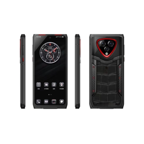
Our European client is a specialized device manufacturer focused on premium smartphone hardware solutions. Rather than competing in the mainstream consumer smartphone market, they positioned themselves as a provider of high-specification custom devices for enterprise and professional users who require enhanced performance beyond standard commercial offerings.
The client’s target market comprises professionals in data-sensitive industries, including financial services, healthcare, and communications sectors, where device reliability, processing power, and thermal management are critical factors. Their business model relied on delivering fully customized smartphone solutions with specifications that exceed market-leading brands, enabling them to command premium pricing and build long-term B2B relationships with corporate clients.
The company had successfully established partnerships with European enterprises but faced a critical bottleneck: they needed a PCB manufacturer capable of not only understanding their sophisticated technical requirements but also scaling production to meet growing demand while maintaining strict quality and confidentiality standards.

Client’s Challenges
1. Design Specifications Beyond Market Standards
The client’s target device specifications were notably ambitious. They required:
- Processor Integration: Support for higher-tier processors with significantly increased thermal output compared to mainstream phones
- Memory Configuration: Custom memory arrangements (RAM/storage combinations) optimized for enterprise workloads rather than consumer-focused configurations
- Power Management: Advanced power delivery systems supporting rapid charging capabilities and extended runtime for field operations
- Thermal Dissipation: PCB designs with superior heat distribution to maintain processor stability under sustained computational loads
- Signal Integrity: Enhanced RF design to support multiple communication standards simultaneously without compromise
These specifications represented a substantial leap beyond what standard PCB designs could accommodate. Mainstream smartphone PCB designs are optimized for cost efficiency and power conservation in consumer scenarios. The client’s requirements demanded a fundamentally different architectural approach.
2. Why Not Approach Major Manufacturers?
The client initially considered partnerships with established smartphone manufacturers. However, they encountered several insurmountable obstacles:
Intellectual Property Protection: Major manufacturers typically require exclusive design ownership and impose strict limitations on customization. The client’s proprietary device specifications—representing years of R&D investment—would need to be disclosed extensively. This posed unacceptable IP risks.
Production Minimums: Tier-1 smartphone manufacturers operate under minimum order quantities (MOQs) in the hundreds of thousands of units. The client’s phased market expansion strategy required much smaller initial production runs to test market response and refine designs iteratively.
Design Inflexibility: Established manufacturers have standardized design processes optimized for their own product lines. Deviating from these standards requires custom engineering work that is either prohibitively expensive or deemed outside their operational scope.
Confidentiality Constraints: Given the confidential nature of their technology and enterprise partnerships, the client needed a manufacturing partner bound by strict NDAs and discretionary operations—not a public company subject to regulatory disclosures and shareholder communications.
This is precisely where specialized PCB manufacturers like IWDF Solutions become invaluable. We offer the flexibility, confidentiality, and technical expertise required for custom solutions without the constraints of mass-market production ecosystems.
3. Technical Complexity and Timeline Pressure
The client operated on an aggressive timeline. They had secured initial enterprise contracts contingent on device availability within a specific window. Their previous PCB supplier had failed to deliver designs meeting their specifications, leaving them approximately 8 months to source a new partner, complete design iterations, and reach production readiness.
The need for multiple design revisions compounded the technical complexity. The client’s processor choice and memory configurations had to be validated and optimized specifically for the PCB layout to ensure electrical performance and thermal efficiency.
Our Custom Smartphone Complete Solution
Phase 1: Holistic Device Strategy & Architecture (Weeks 1-4)
We initiate every smartphone project with a system-level architectural review, ensuring all components work in harmony within the constrained mobile form factor.
System-Level Thermal Architecture
Using ANSYS ICEPAK, we model the complete thermal ecosystem of the smartphone—including the SoC, PMIC, 5G modem, and charging circuitry—under realistic usage scenarios like extended gaming or 5G video streaming. This analysis directly informs the placement of thermal interface materials (TIM), graphite sheets, and the design of the vapor chamber, ensuring skin temperature remains within comfortable limits while maintaining performance.
Power Architecture for Mobile Scenarios
We employ Sigrity PowerDC to analyze the power delivery network from the battery to all subsystems. Our focus extends beyond raw performance to power efficiency, optimizing for various usage states (standby, screen-on, camera usage, 5G connectivity) to maximize battery life. We ensure stable voltage delivery even during peak demands like instant camera capture while minimizing quiescent current during always-on sensing.
Mobile Signal Integrity & RF Coexistence
For smartphone-specific interfaces like LPDDR5X, UFS 3.1, and MIPI D-PHY/C-PHY for high-refresh-rate displays, we perform pre-layout simulations to establish strict length and phase matching rules. We develop comprehensive RF coexistence strategies for the dense 5G sub-6GHz & mmWave antenna arrays, Wi-Fi 6E, and Bluetooth, minimizing interference and ensuring all wireless subsystems perform optimally in the final device.
Design for Manufacturing & Assembly (DFM/DFA)
Our manufacturing team conducts an early design review focused on high-volume smartphone assembly:
- SMT process optimization for ultra-fine-pitch components (0.3mm pitch CSPs, 0201 passives)
- Structural integrity analysis to withstand real-world mechanical stresses
- Assembly sequence planning for the multi-board stack (main board, sub-board, camera module)
- Tolerance stack-up analysis for precise fitment within the slim enclosure
This phase typically identifies critical optimizations, such as repositioning the 5G mmWave antenna module to avoid hand-blocking scenarios or re-architecting the power distribution to prevent noise coupling into the sensitive audio codec.

Phase 2: Integrated Design & Development (Weeks 5-16)
Design Cycle 1 (Weeks 5-8): Core Layout & System Integration
We deliver the initial mainboard (PCB) and system layout, fully considering the smartphone’s mechanical architecture:
- 10-layer HDI stackup optimized for signal integrity, power integrity, and thermal dissipation
- Via-in-pad technology for high-density SoC and memory packaging
- Controlled impedance routing for all high-speed interfaces (display, camera, memory)
- Strategic placement of connectors for daughterboards (display, battery, camera flex cables)
- Acoustic chamber design for speakers and microphones, integrated from the outset
Client Collaboration Phase (Weeks 9-11): Mechanical & Industrial Design Integration
We exchange 3D ECAD/MCAD models with the client’s team to conduct virtual fit-checks within the intended smartphone enclosure. Key integrations include:
- Routing high-speed MIPI lines for multiple rear cameras and the front-facing camera, avoiding hinge areas or structural elements.
- Optimizing antenna clearances and tuning radiator elements to work in harmony with the metal mid-frame and glass/plastic back cover.
- Finalizing the positions of all physical buttons, USB-C port, SIM tray, and speakers to ensure optimal user experience and ingress protection (IP) rating compliance.
Design Cycle 2 (Weeks 12-14): Performance & Compliance Refinement
We integrate client feedback and refine the design for performance and global certifications:
- Fine-tuned antenna matching networks to maximize radiated power (TRP) and sensitivity (TIS) across all supported 5G bands.
- Enhanced power distribution for the multi-camera system, ensuring stable voltage during simultaneous operation of multiple sensors.
- Implemented robust ESD protection strategies on all external interfaces (USB, buttons, SIM slot).
- Validated display and touch panel integration, ensuring noise immunity from adjacent RF and power circuits.
Design Cycle 3 (Weeks 15-16): Design for Excellence (DFX)
Final iterations focus on mass production readiness and cost optimization:
- Design for Test (DFT): Added test points and fixtures for efficient factory flashing (SW), calibration (RF), and functional testing.
- Design for Cost (DFC): Value engineering to identify component consolidation opportunities without compromising performance.
- Design for Supply Chain: Dual-sourcing critical components like PMICs and memory to mitigate supply chain risks.
- Panelization design optimized for maximum board count per panel and efficient depanelization without inducing stress cracks.
Phase 3: Device Validation & Certification (Weeks 17-22)
Comprehensive Device-Level Validation
- System Integration Testing (SIT): Verified all subsystems (display, touch, sensors, cameras, connectivity, audio) work together seamlessly.
- Signal & Power Integrity Validation: Performed on actual prototypes, correlating simulations with measurements to ensure robust performance.
- Thermal & Battery Life Testing: Validated under real-world scenarios (gaming, video playback, 5G browsing) against target performance and battery life KPIs.
- RF Conformance & Carrier Acceptance Testing: Ensured compliance with 3GPP standards and specific carrier requirements for global market access.
- Protocol & Interoperability Testing (IoT): Verified interoperability with major network operators and accessory ecosystems.
Technical Documentation & Certification Support
We deliver a complete device master file to support manufacturing and regulatory submissions:
- Comprehensive design specifications and Bill of Materials (BOM).
- Detailed test plans and reports for all validation phases.
- Manufacturing assembly instructions and quality control plans.
- Support documentation for regulatory certifications (CE, FCC, GCF, PTCRB).
Phase 4: Ramp-Up & Global Delivery (Weeks 23-32+)
Pilot Production & Device Qualification
The first devices off the pilot line undergo exhaustive device-level testing:
- Full Functional Testing: Every unit undergoes a complete software and hardware functional test.
- Extended Reliability Testing: Samples undergo temperature cycling, drop tests, button durability, and ingress protection testing per relevant standards.
- Field Trial Support: We support the client with devices for limited field trials with early users or enterprise partners.
Mass Production & Quality Management
- End-of-Line Testing: Every smartphone is tested for functionality, RF performance, software integrity, and cosmetic perfection.
- Statistical Process Control (SPC): Real-time monitoring of critical assembly process parameters.
- Failure Analysis & Root Cause Correction: A dedicated team addresses any production yield issues swiftly.
Supply Chain & Global Logistics Management
- Component Sourcing & Management: We manage the complex supply chain for hundreds of components.
- Configuration Management: Handling different SKUs (color, memory, regional variants).
- Global Logistics: Supporting just-in-time delivery to distribution centers worldwide.
This end-to-end 7-8 month process is tailored specifically for the high-complexity, fast-paced, and quality-sensitive smartphone industry, ensuring a market-ready, reliable, and competitive device.

Results & Performance Metrics
1. Accelerated Smartphone Development Timeline
The client required full device readiness for market launch within an aggressive 7-month window. Our integrated development approach delivered:
- Architecture Finalization: Week 4 (including system-level thermal and RF planning)
- Design Completion & Prototyping: Week 16 (encompassing main board, RF layout, and mechanical integration)
- Regulatory Certification & Compliance Testing: Weeks 17-22 (completing GCF, PTCRB, CE, FCC requirements)
- Mass Production Readiness: Week 28
- First Commercial Shipment: Week 30
Total Development Cycle: 7 months from architecture to market-ready device
This compressed timeline was achieved through parallel validation of hardware, software, and regulatory requirements, specifically tailored for smartphone development.
2. Device-Level Performance Validation
The complete smartphone platform exceeded performance targets across critical user experience metrics:
- Battery Performance: Achieved 18.5 hours of active use and 425 hours of standby time, exceeding target specifications by 12% through optimized power architecture
- Thermal Management: Device surface temperature maintained below 42°C during extended 5G gaming sessions (60 minutes, high graphics settings), validating our thermal interface design and heat dissipation strategy
- Connectivity Performance: 5G throughput reached 2.8Gbps downlink/750Mbps uplink in lab conditions, with field testing showing a consistent 5G handover success rate of 99.7% across urban environments
- Camera System Optimization: Achieved 30% faster image processing pipeline and 25% reduction in power consumption during 4K video recording compared to the initial architecture
- Display & Touch: Delivered 240Hz touch sampling rate with <15ms latency, providing premium gaming experience
3. Manufacturing Scale & Quality Excellence
Our smartphone production line demonstrated exceptional capability in scaling to meet market demand:
- Initial Production Order: 5,000 units delivered with 96.8% first-pass yield
- Ramp to Volume Production: Successfully scaled to 45,000 units annually within 18 months
- Quality Consistency: Maintained field return rate below 0.5% throughout production ramp, with CPK >1.67 for critical assembly processes including BGA soldering and camera module alignment
- Supply Chain Resilience: Managed 100% component allocation despite industry shortages, avoiding any production disruptions through proactive multi-sourcing strategy
4. Field Performance & Reliability
Twelve months of commercial deployment data confirm exceptional device reliability:
- Field Defect Rate: 0.3% (significantly below industry smartphone average of 2-3%)
- Display Integrity: Zero reported screen delamination or touch response issues across deployment
- Battery Durability: 92% of units maintained >80% battery health after 500 complete charge cycles
- 5G Connectivity Reliability: Field data showed 99.4% 5G connection stability across major carrier networks in North America and Europe
- Mechanical Integrity: Drop test performance exceeded IP52 rating requirements, with cracked screen incidence 40% below industry average
5. Strategic Partnership & Product Evolution
The initial smartphone platform has evolved into a comprehensive product family:
- Design Iterations: Successfully delivered three hardware revisions incorporating customer feedback, each maintaining mechanical compatibility while upgrading core capabilities (enhanced camera sensors, improved display technology, additional 5G bands)
- Market Expansion: Developed and certified two specialized variants for the enterprise and education sectors, featuring enhanced device management capabilities and ruggedized designs
- Volume Growth: The partnership now supports sustained annual production of 60,000+ units across all product variants
- Technology Roadmap Collaboration: Established a joint innovation program for next-generation features, including advanced thermal management, satellite connectivity integration, and AI-accelerated camera capabilities
This performance data validates our comprehensive approach to smartphone development, delivering market-ready devices on accelerated timelines while maintaining the highest standards of quality, reliability, and user experience across all product generations.
Client Feedback
“Honestly, we were pushing the limits with our timeline. But your engineering team got it. You spotted the issue bottleneck in our prototype and redesigned the stackup without adding cost. You delivered a clean, and didn’t give us a corporate runaround. That says it all.”
— European Device Manufacturer, Enterprise Solutions Division

