

Multilayer PCBs represent the backbone of modern electronics—from automotive control systems to medical devices and industrial automation platforms. Yet when engineers face the need to reverse engineer these complex boards, they quickly encounter challenges that single or double-layer boards simply don’t present. Whether driven by obsolete component replacement, design legacy recovery, competitive analysis, or critical failure investigation, the complexity multiplies exponentially with each additional layer.
The reality is straightforward: a six-layer or eight-layer PCB with buried and blind vias, high-density interconnections, and miniaturized components requires specialized knowledge, precision instrumentation, and structured workflows that go far beyond basic reverse engineering techniques. For global manufacturers seeking reliable reconstruction data that translates directly into production-ready designs, understanding these five core challenges—and how experienced professionals systematically overcome them—becomes essential to project success, risk mitigation, and accelerated time-to-production.
This guide walks through the specific obstacles that make multilayer PCB reverse engineering complex, the practical methodologies that professionals employ to address them, and the concrete deliverables that ensure accurate, manufacturable outcomes.
The Five Core Challenges
Before diving into detailed solutions, here’s a concise overview of the barriers that consistently shape multilayer PCB reverse engineering projects:
- Complex hidden layer structures and stacking topology – Identifying the number of layers, their order, functionality, and internal interconnection pathways without non-destructive imaging.
- Blind and buried vias, plus internal trace accessibility – Recognizing connections that exist entirely within the board, connecting only internal or surface-to-internal layers, while mapping their routing and impedance characteristics.
- Component identification and BOM reconstruction difficulties – Accurately naming, locating, and cataloging original components when markings are unclear, packages are proprietary, or bottom-side soldering conceals identification data.
- Intellectual property protections and physical access barriers – Navigating potting compounds, conformal coatings, specialized encapsulation, and protective markings that are deliberately designed to resist reverse engineering.
- Ensuring design-to-manufacture accuracy and consistency – Translating high-resolution layer images, internal routing data, and component information into CAD/Gerber files that maintain electrical, mechanical, and thermal integrity across mass production runs.
Deep-Dive Analysis and Professional Solutions
Challenge 1: Complex Hidden Layer Structures and Stacking Topology
The Core Problem
A multilayer PCB with six, eight, or more conductive layers creates a three-dimensional puzzle. Each layer serves a distinct electrical function—signal routing, ground planes, power distribution, or high-frequency impedance control—yet the human eye cannot distinguish them without destructive cross-sectioning or advanced imaging. Determining the total layer count, the order in which they’re stacked, and the electrical role of each layer is the foundational step that drives all subsequent reverse engineering work.
Why This Matters
Layer identification errors cascade through the entire project. Misidentifying whether a layer is a ground plane versus a signal layer leads to incorrect netlist extraction, flawed schematic reconstruction, and ultimately, a non-functional design reproduction. Underestimating layer thickness, substrate material properties, or the presence of embedded components introduces manufacturing tolerances that can render mass-production batches electrically faulty.
Professional Approach
Experienced reverse engineers establish a documented baseline through multiple information sources:
- Non-destructive imaging (X-ray and computed tomography): Modern X-ray fluorescence and X-ray computed tomography (CT) systems generate cross-sectional images revealing layer stacks with micron-level precision. These images show conductive traces, via positions, and component connections without destroying the board. CT imaging particularly excels at revealing layer structure in the Z-axis (vertical cross-section) while maintaining the XY plane detail of trace routing.
- High-resolution photography and microscopy: After careful removal of solder mask and conformal coatings (when permitted), macro photography documents each exposed layer. Color contrast, trace widths, and via patterns become visible references for layer identification and comparison.
- Layer count validation through cross-reference: Cross-checking layer information derived from X-ray imaging against physical thickness measurements, dielectric constant calculations, and PCB stackup industry standards creates multiple validation points. A four-layer board typically measures 1.6mm; a six-layer board 2.4mm; eight-layer board 3.2mm—deviations indicate special stackups or embedded components.
- Electrical property analysis: Measuring impedance characteristics and signal transmission paths on outer layers often reveals the presence and approximate location of inner power or ground planes through high-frequency behavior patterns.


Deliverables for This Phase
- Layer stackup diagram: A detailed cross-sectional drawing showing layer order, material composition (FR-4, polyimide, copper thickness), dielectric thickness, and intended electrical function of each layer.
- Layer-to-layer connectivity reference: A matrix document or visual guide mapping which layers are connected via through-holes or blind/buried vias, and where those connections occur spatially.
- Preliminary CAD sketch: A basic layer representation in CAD software that serves as the working reference for subsequent detailed reconstruction work.
Challenge 2: Blind and Buried Vias, Plus Internal Layer Accessibility
The Core Problem
Through-hole vias (which penetrate the entire PCB thickness from top to bottom layer) are relatively straightforward to identify through basic visual inspection. However, modern high-density designs frequently employ blind vias (connecting outer layers to one or more inner layers, but not through the entire board) and buried vias (connecting only internal layers, completely invisible from the outside). These hidden interconnections represent critical signal paths, power distribution, and ground stitching—yet they are invisible without advanced sectioning or imaging techniques.
Identifying the exact start layer, end layer, and lateral position of each blind or buried via is essential for accurate netlist extraction and schematic reconstruction. Misidentifying or omitting even a single internal via can break signal integrity, create unintended ground faults, or introduce impedance mismatches.
Why This Matters
Blind and buried vias enable modern PCB designs to achieve higher component density and faster signal propagation in space-constrained environments (smartphones, wearables, high-speed networking equipment). However, they also create ambiguity during reverse engineering. A designer analyzing the outer layer alone cannot determine whether a via extends only to Layer 3, or connects all the way to Layer 6. This ambiguity must be resolved through systematic imaging and analysis.
Professional Approach
Professionals employ a multi-modal strategy:
- X-ray imaging with advanced contrast enhancement: Sequential X-ray images at different vertical planes (Z-axis slicing) can reveal the top and bottom endpoints of blind and buried vias. By adjusting the X-ray beam angle and taking multiple passes, technicians build a 3D map of internal via positions and their layer-to-layer span.
- Precision layer-by-layer delayering and optical imaging: In cases where non-destructive imaging alone is insufficient, controlled chemical or mechanical delayering removes thin material increments (10-25 microns) from the board surface. After each removal step, high-resolution photography documents the newly exposed layer. This process, conducted methodically, creates a sequential dataset showing via positions across multiple layers without damaging intact internal structures.
- Electrochemical potential mapping: Applying electrical stimuli to specific layer-to-layer connection points and measuring electrical potential differences helps reverse engineers confirm which layers are electrically connected through which vias, even when visual confirmation is ambiguous.
- Netlist extraction automation: Advanced software scans X-ray or optical layer images, identifies via pads and their interconnections, and generates an automated netlist. While not 100% accurate, this software-assisted approach accelerates identification of candidate connections that technicians then manually verify.
Deliverables for This Phase
- Via connectivity diagram: A detailed reference showing the location (x, y coordinate), starting layer, ending layer, estimated via diameter, and electrical function (signal, power, ground) of each identified via.
- Layer-by-layer dissection photographs: High-resolution images of each layer after delayering, annotated with via positions and trace routing for verification and record-keeping.
- Internal trace routing map: A document or CAD overlay showing the path of signal traces and power distribution across internal layers, especially highlighting connections that traverse multiple layers through blind/buried vias.
- Continuity verification report: A detailed record of electrical testing results confirming which layer pairs are electrically connected and the measured resistance/impedance of those connections.
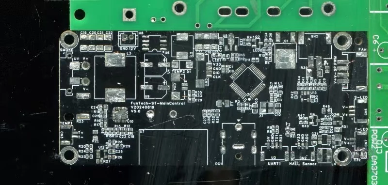
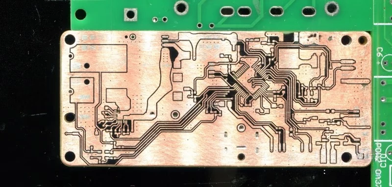
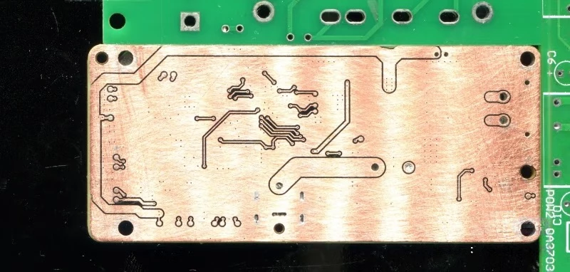
Challenge 3: Component Identification and Bill of Materials Reconstruction
The Core Problem
A densely populated multilayer PCB may carry hundreds of components—resistors, capacitors, inductors, integrated circuits, and specialized modules—each requiring accurate identification by part number, value, package type, and orientation. Modern components often share identical physical packages (e.g., dozens of different integrated circuits in BGA or QFN packages), making visual identification impossible without manufacturer markings.
The challenge intensifies when markings are faint, obscured by potting compound, or deliberately obfuscated. Bottom-side component pads are often soldered first (wave soldering, reflow), leaving them inaccessible for visual inspection once the top side is assembled. Proprietary or legacy components may no longer carry consistent marking standards, or markings may have been deliberately altered to protect intellectual property.
Why This Matters
An incomplete or inaccurate BOM (Bill of Materials) renders the entire reverse engineering project unreliable. A designer attempting to reproduce the board will select substitute components with different electrical characteristics, package sizes, or performance ratings. This inevitably leads to functional failures, thermal mismanagement, signal integrity violations, or assembly incompatibilities when scaling to mass production.
Professional Approach
Reverse engineering professionals combine multiple identification methodologies:
- Visual inspection and marking decoding: Technicians photograph and decode component markings using industry reference libraries (date codes, manufacturer logos, alphanumeric part codes). Specialized databases cross-reference abbreviated markings to full part numbers.
- Component characteristic fingerprinting: When markings are absent or unclear, physical measurements become identifying clues. Measuring component leads, body dimensions, pin pitch, and weight often narrows candidates to a small group. Electromagnetic properties (inductance, capacitance) and thermal response profiles further refine identification.
- Reverse CAD and schematic analysis: Once the schematic topology is partially reconstructed from netlist extraction, functional roles of components become apparent. A component connected between power and ground in a high-current path is likely a bulk capacitor; a component in series with a high-speed clock line likely has controlled impedance characteristics. This functional context guides component selection and identification.
- Decapsulation and microanalysis (where legally and technically feasible): For critical proprietary ICs or specialized components, controlled decapsulation reveals internal die markings, manufacturing dates, and sometimes alternate part number information. This approach is expensive and destructive, but necessary in high-value reverse engineering projects.
- Cross-reference with design intent: Analyzing PCB layout patterns, trace routing priorities, and thermal management strategies often reveals the intended component complement. High-frequency bypass capacitors typically cluster near IC power pins; electrolytic storage capacitors occupy corner positions; specialized connectors dictate board-edge traces.
Deliverables for This Phase
- Component reference list: A comprehensive table with reference designator (R1, C2, U3), component type, identified part number, package type, value/rating, quantity, and confidence level for each identification.
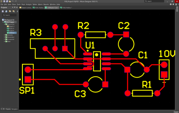
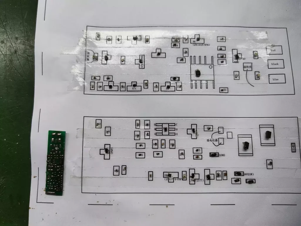
- Annotated placement diagram: A top and bottom view of the PCB with all components labeled by reference designator, highlighting components where identification confidence is lower or where alternate part numbers exist.
- Component sourcing and substitution notes: A detailed guide documenting which original components are still in production, which are obsolete (with recommended replacements), and which require special sourcing due to rarity or proprietary nature.
- BOM validation checklist: A cross-check document confirming component totals by type, functional groupings (power management ICs, analog interfaces, digital controllers), and sourcing feasibility for mass production.
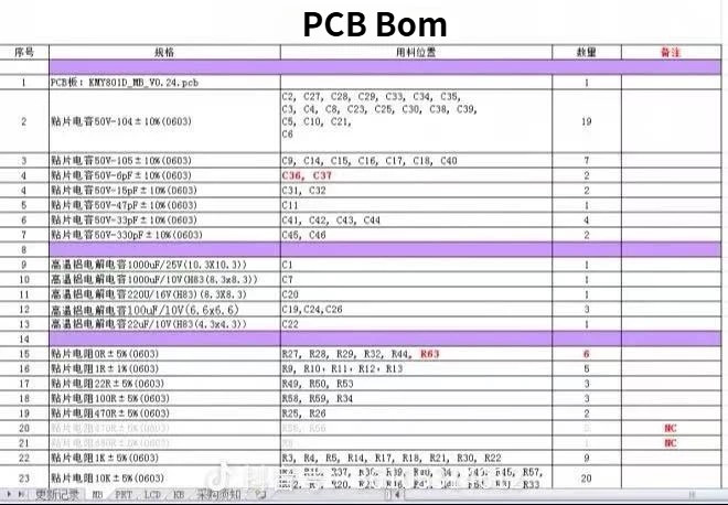
Challenge 4: Intellectual Property Protection and Physical Access Barriers
The Core Problem
Modern PCBs often incorporate deliberate protective measures designed to resist or hinder reverse engineering. These include conformal coatings (acrylic, urethane, parylene), potting compounds (epoxy, polyurethane), specialized encapsulation, selective silkscreen obfuscation, and deliberate routing choices that obscure functional blocks. Additionally, many high-value boards integrate proprietary ASICs, application-specific components, or encrypted firmware that cannot be functionally replicated without understanding their internal operation—and manufacturers intentionally obscure this information to protect trade secrets.
The reverse engineering professional must navigate not only the technical challenge of accessing hidden information, but also the legal and ethical landscape surrounding intellectual property, trade secrets, and rightful repair/replacement rights.
Why This Matters
Attempting to bypass physical access barriers (via aggressive chemical removal or destructive sectioning) without clear legal authorization can violate intellectual property laws, trade secret protections, and contract terms. Simultaneously, legitimate reverse engineering for repair, obsolescence replacement, or interoperability purposes has specific legal protections in many jurisdictions. Clarifying this boundary upfront prevents costly project delays, legal disputes, or project abandonment.
Professional Approach
Experienced service providers implement a structured compliance and technical risk assessment:
- Legal and compliance pre-project review: Before technical work begins, a comprehensive evaluation determines whether the reverse engineering project falls within legally protected categories (repair of owned equipment, replacement of obsolete components, interoperability, educational research). Documentation is gathered confirming project legitimacy, ownership status, and applicable jurisdictional protections. This review identifies potential intellectual property risks and establishes clear boundaries on what technical approaches are permissible.
- Risk classification matrix: Physical components and functional blocks are categorized by reverse engineering difficulty, legal risk, and functional replaceability. High-risk elements (encrypted firmware, patented ASIC designs) are flagged for reduced priority or alternative solution approaches. Lower-risk elements (commodity passive components, standard connectors) proceed with full reverse engineering effort.
- Non-destructive imaging prioritization: Before resorting to destructive delayering, potting removal, or decapsulation, technicians maximize the information extracted through X-ray, CT, thermal imaging, and electromagnetic analysis. These techniques often yield sufficient data without triggering IP concerns or physical damage.
- Functional analysis and black-box substitution: Rather than attempting to replicate proprietary components by reverse engineering their internals, engineers analyze their external behavior (electrical characteristics, timing, signal protocols) and identify commercially available alternatives that provide equivalent functionality. This “behavioral reverse engineering” often achieves project goals while respecting IP boundaries.
- Documentation and audit trail: All technical decisions, legal considerations, and risk assessments are documented comprehensively. This audit trail demonstrates good-faith compliance efforts and protects both the service provider and the client in case of legal scrutiny.
Deliverables for This Phase
- IP and compliance assessment report: A detailed evaluation of project legitimacy, applicable legal frameworks (repair rights, DMCA exemptions, right-to-repair regulations), identified risks, and recommended technical approaches that respect IP boundaries.
- Risk categorization matrix: A visual or tabular reference identifying high-risk components/blocks, recommended substitution or workaround strategies, and expected challenges in achieving functional equivalency.
- Functional equivalency analysis: For components that cannot be reverse engineered due to IP concerns, a technical specification document outlining required electrical behavior, interface protocols, and performance characteristics—guiding selection of alternative solutions.
- Compliance and audit documentation: A comprehensive record of all compliance reviews, legal considerations evaluated, and decisions made—serving as evidence of reasonable, good-faith reverse engineering practices.

Challenge 5: Ensuring Design-to-Manufacture Accuracy and Consistency
The Core Problem
The final challenge in multilayer PCB reverse engineering is translating vast amounts of imaging data, netlist information, and component details into a complete, manufacturable PCB design (CAD files, Gerber format, drill files, and production specifications). This step demands absolute precision: a trace routing error of a few mils, a missing ground connection, or an incorrect layer assignment can result in manufacturing defects, electrical failures, or complete product non-functionality.
Additionally, the original design may have been optimized for specific manufacturing capabilities of its original producer. When reverse engineers reconstruct that design for a different manufacturer or different production scale, design adjustments become necessary to match new manufacturing capabilities, minimum feature sizes, and cost structures—while maintaining electrical and mechanical integrity.
Why This Matters
Even if all previous challenges are perfectly solved—accurate layer identification, complete via mapping, correct BOM—a flawed translation to CAD and manufacturing files renders the entire project unsuccessful. Conversely, a meticulous design-to-manufacture process ensures first-pass production success, eliminates costly respins, and enables rapid scaling from pilot batches to high-volume production.
Professional Approach
Professionals employ systematic CAD reconstruction and Design-for-Manufacturability (DFM) processes:
- Systematic CAD reconstruction with verification gates: Layer images are imported into professional CAD software (Allegro, Altium, KiCad) and meticulously redrawn. After each section (layer-by-layer trace routing, via placement, component footprints), a verification step compares the CAD recreation against the original images. Automated tools overlay CAD traces against high-resolution photographs, highlighting discrepancies that require correction.
- Netlist extraction and schematic reconstruction: Automated netlist extraction tools analyze the CAD layer data and generate connection lists. These are cross-referenced against manual netlist data captured during Layer 2’s via analysis and Layer 3’s component identification. Discrepancies between automated and manual netlists are investigated and reconciled before proceeding to schematic capture.
- DFM analysis and manufacturability assessment: The reconstructed design is subjected to rigorous Design-for-Manufacturability review against the target manufacturer’s capabilities. This evaluation covers:
- Minimum trace width and spacing – Ensuring design rules comply with manufacturer tolerances (typically 4-5 mils minimum for standard PCBs, finer for specialized processes).
- Via diameter and aspect ratio – Verifying that via sizes and the ratio of via depth to diameter fall within manufacturing capability windows.
- Layer stack-up optimization – Confirming that the reconstructed stackup achieves necessary electrical impedance, thermal management, and mechanical stability.
- Component density and assembly feasibility – Ensuring that component placement, pitch, and accessibility support production assembly without yield loss.
- Thermal and electrical testing points – Identifying adequate access for production testing, functional verification, and thermal profiling.
- Simulation and electrical verification: The reconstructed schematic and PCB layout are subjected to electrical simulation (SPICE for analog circuits, logic simulation for digital designs, signal integrity analysis for high-speed traces). Simulated performance is compared against original board measurements and documented specifications. Discrepancies indicate either reverse engineering errors or design optimizations necessary for the new manufacturer.
- First-article inspection and prototype correlation: A limited production run (typically 5-10 boards) is manufactured using the reconstructed design. Functional testing, dimensional measurement, and thermal profiling are compared against known good boards from the original production run. Correlation typically targets 95%+ electrical and 99%+ mechanical compliance.
Deliverables for This Phase
- Complete CAD database: Full schematic, PCB layout, and layer definitions in industry-standard formats (IPC-2581, Gerber X2, ODB++) compatible with high-volume PCB manufacturers.
- Gerber and drill file package: Production-ready manufacturing files including top/bottom copper, internal signal layers, solder mask, silkscreen, and mechanical assembly drawings.
- Bill of Materials with sourcing: Comprehensive parts list with manufacturer part numbers, package types, approved supplier sources, alternative parts (where applicable), and lead-time estimates.
- Manufacturing specifications: Detailed documentation including stackup definition, trace width/spacing, via specifications, impedance targets, surface finish, plating requirements, and testing criteria.
- DFM analysis report: A thorough evaluation of manufacturability, identified risks, recommended design optimizations, and expected manufacturing yield targets.
- Functional test specification and results: A documented test plan for prototype validation, measured results from first-article boards, and correlation analysis against original designs.

IWDF Solutions’ End-to-End Multilayer PCB Reverse Engineering Workflow
Understanding the five core challenges is essential. However, translating that knowledge into consistent, reliable project execution requires a structured, repeatable workflow with clear handoff points, quality gates, and documented deliverables. This section outlines IWDF Solutions’ approach to systematically managing multilayer PCB reverse engineering from initial inquiry to production-ready design and scaled manufacturing.
Stage 1: Project Initiation and Feasibility Assessment
Objective: Confirm project legitimacy, scope, technical feasibility, timeline, and initial risk factors.
Activities:
- Initial consultation capturing target board specifications, business drivers, volume requirements, and delivery timeline.
- Intellectual property review, including contract review, ownership documentation, and compliance assessment against applicable regulations (DMCA, right-to-repair laws, trade secret protections).
- Physical examination of the sample board including layer count assessment, component density evaluation, and preliminary complexity rating.
- Non-disclosure agreement (NDA) execution and security protocols establishment.
Deliverables:
- Feasibility assessment report confirming project viability.
- Preliminary complexity and timeline estimate.
- Compliance statement and risk disclosure.
- Project execution roadmap with defined milestones.
Timeline: Typically 3-5 business days.
Stage 2: Comprehensive Data Acquisition and Layer Structure Confirmation
Objective: Generate complete visual and electrical datasets capturing every aspect of the physical PCB structure.
Activities:
- High-resolution photography (minimum 5MP) of top side, bottom side, and edge profiles at multiple magnification levels.
- X-ray computed tomography imaging capturing full 3D layer structure, internal trace routing, and via positioning.
- Precision measurement of board dimensions, thickness, and component heights.
- Non-destructive electrical characterization including impedance measurements, continuity testing, and signal path tracing.
- Conformal coating or potting compound assessment for feasibility of selective removal (where legally permissible and technically necessary).
Deliverables:
- High-resolution photograph archive (minimum 200+ images).
- X-ray CT volumetric dataset with layer-by-layer cross-sectional imagery.
- Physical measurement documentation and preliminary stackup hypothesis.
- Electrical characterization dataset and initial netlist candidates.
Timeline: Typically 5-7 business days.
Stage 3: Layer Reconstruction and Internal Connectivity Mapping
Objective: Establish definitive layer structure via connectivity and internal trace routing.
Activities:
- Systematic analysis of X-ray imagery, generating preliminary layer count confirmation and stackup hypothesis.
- Controlled delayering (when necessary and permitted) with optical imaging after each removal increment.
- Via mapping utilizing multi-angle X-ray imaging, optical microscopy, and electrical continuity testing.
- Cross-layer connectivity verification using netlist extraction software combined with manual validation.
- Internal trace routing documentation for all signal, power, and ground paths.
Deliverables:
- Definitive layer stackup diagram with material composition and electrical function.
- Via connectivity reference matrix showing start layer, end layer, position, and function for every identified via.
- Complete internal trace routing map, layer-by-layer.
- CAD layer structure template ready for detailed trace reconstruction.
Timeline: Typically 7-10 business days, depending on layer count and complexity.
Stage 4: Component Identification and BOM Compilation
Objective: Generate a complete, accurate Bill of Materials with verified part numbers, packages, and sourcing information.
Activities:
- Systematic component-by-component identification using visual marking analysis, characteristic fingerprinting, and cross-reference databases.
- Component location and orientation documentation with high-resolution placement photography.
- Functional analysis linking identified components to circuit blocks and schematic roles.
- Sourcing research confirming part number validity, current production status, and alternative availability.
- Obsolescence analysis for legacy components, with recommended modern equivalents where applicable.
Deliverables:
- Comprehensive BOM with reference designator, part number, package type, quantity, sourcing status, and substitution recommendations.
- Annotated placement diagram (top and bottom views) with all components labeled.
- Component identification confidence assessment (high/medium/low for each part).
- Sourcing feasibility report and lead-time estimates.
Timeline: Typically 5-8 business days, depending on component count and identification challenges.
Stage 5: DFM Evaluation and Production Feasibility Analysis
Objective: Assess the target manufacturer’s capability to produce boards matching the reconstructed design, identify necessary design optimizations, and confirm producibility.
Activities:
- Detailed DFM review against IWDF’s manufacturing capabilities and design rules (4-mil trace/spacing, via diameter ranges, layer stackup options, surface finishes).
- Thermal management analysis identifies heat dissipation paths and potential thermal stress points.
- Manufacturing yield risk assessment and corrective design modifications where necessary.
- Prototype build planning, including component sourcing, first-article inspection criteria, and functional test specification.
Deliverables:
- DFM analysis report with identified risks and recommended design modifications.
- Manufacturing capability matrix confirming feasibility for the target volume.
- Thermal analysis and management strategy.
- Prototype build plan and first-article inspection criteria.
Timeline: Typically 3-5 business days.
Stage 6: CAD Reconstruction and Manufacturing File Generation
Objective: Translate all reverse engineering data into complete, production-ready CAD and manufacturing files.
Activities:
- Schematic capture based on netlist extraction and functional analysis, with voltage node identification and signal labeling.
- PCB layout recreation from layer imagery, with systematic verification against original high-resolution photographs.
- Automated design rule checking (DRC) and netlist verification, ensuring no floating nets or unconnected nodes.
- Gerber, drill file, and ODB++ generation in formats compatible with high-volume manufacturers.
- Documentation package compilation, including stackup definition, material specifications, and assembly drawings.
Deliverables:
- Complete schematic diagram (PDF and editable CAD format).
- PCB layout in native CAD format (Allegro, Altium, or equivalent).
- Manufacturing output files: Gerber X2, NC drill, ODB++.
- Bill of Materials with manufacturer part numbers and alternative sources.
- Manufacturing specification document covering stackup, trace/spacing rules, surface finish, and testing criteria.
Timeline: Typically 7-10 business days.
Stage 7: Prototype Manufacturing and First-Article Verification
Objective: Validate the reconstructed design by manufacturing a limited pilot run and verifying electrical and mechanical compliance with originals.
Activities:
- Pilot PCB manufacturing run (typically 5-10 units) using standard manufacturing processes.
- Component procurement and board assembly match production planned processes.
- Dimensional verification (board size, hole positions, thickness) against original specifications.
- Electrical functional testing comparing the prototype against known-good original boards.
- Thermal profiling and power consumption measurement.
- Detailed documentation of any discrepancies or out-of-spec conditions.
Deliverables:
- First-article inspection report with dimensional and electrical measurements.
- Functional test results and comparison against original board performance.
- Corrected CAD files and manufacturing documentation (if modifications required).
- Sign-off on design accuracy and manufacturability.
Timeline: Typically 10-14 days (including manufacturing and assembly lead time).
Stage 8: Design Refinement and High-Volume Production Readiness
Objective: Finalize all design documentation, establish production processes, and prepare for scaled manufacturing.
Activities:
- Incorporation of any prototype feedback or design modifications.
- Final design review and engineering sign-off.
- Production process documentation, including assembly sequence, test points, and quality control checkpoints.
- Supplier quality agreement (SQA) establishment with component vendors.
- Initial orders for production tooling, fixture development (if applicable), and test equipment calibration.
Deliverables:
- Final approved design package (schematic, PCB layout, manufacturing files).
- Complete technical documentation for the production team.
- Production cost estimate and quotation for volume manufacturing.
- Quality assurance and test procedure documentation.
Timeline: Typically 5-7 business days.


Real-World Application and Trust Factors
The challenges and solutions outlined above represent genuine technical and operational realities that IWDF Solutions addresses routinely across global customer projects. Practical experience across multiple industries—consumer electronics, automotive systems, industrial automation, medical devices, and telecommunications—has refined IWDF’s approach to ensure consistent success even in highly complex scenarios.
Industry-Specific Insights
Consumer Electronics: In this sector, product lifecycle pressure and competitive obsolescence frequently drive reverse engineering needs. Legacy smartphone components, display controllers, and power management ICs often require precise reproduction to continue supporting installed user bases. IWDF has successfully reconstructed designs ranging from 4-layer phone charging circuits to 12-layer camera module controllers, managing rapid iteration and high-volume scaling.
Automotive and Industrial Control: Safety-critical applications demand extremely high accuracy and traceability. Automotive engine control modules, transmission controllers, and industrial PLC boards require not only functional reproduction but also detailed documentation of design intent, component stress ratings, and failure-mode analysis. IWDF’s comprehensive documentation and first-article verification processes ensure automotive-grade quality (ISO TS 16949 compliance) across every reconstruction project.
Medical Devices: Regulatory requirements in medical device manufacturing demand complete design history files, biocompatibility documentation, and rigorous traceability. IWDF’s reverse engineering process captures all necessary data for FDA/CE/PMDA regulatory submissions, enabling legacy device manufacturers to transition designs to new suppliers while maintaining regulatory compliance and patient safety.
Trust and Credibility Factors
IWDF Solutions’ position as a trusted reverse engineering and manufacturing partner is grounded in several key differentiators:
- In-House Manufacturing Capability: Unlike many consulting-only firms, IWDF operates complete PCB design, prototyping, and high-volume manufacturing facilities. This end-to-end integration ensures that reverse engineering outputs are immediately manufacturable, reducing costly redesigns and accelerating time-to-market.
- International Certifications: IWDF maintains ISO 9001 quality management, ISO 13485 medical device manufacturing, ISO TS 16949 automotive quality, and IPC-A-610 workmanship standards. These certifications represent third-party verification of process discipline and quality consistency.
- Multi-Language Technical Support: Global customer bases require multilingual project communication. IWDF provides English, Mandarin Chinese, and German technical support, ensuring clarity across international teams.
- Secure Data Handling and Confidentiality: All reverse engineering data is processed under strict confidentiality agreements, secure network infrastructure, and documented chain-of-custody procedures. Physical samples and design data are stored in locked, climate-controlled facilities with restricted access logging.
- Long-Term Customer Relationships: IWDF has maintained multi-year partnerships with global Fortune 500 companies, regional manufacturers, and specialized boutique firms. Repeat customer rates exceed 75%, reflecting consistent delivery of high-quality, accurate designs and reliable manufacturing partnerships.
- Transparent Risk Communication: Rather than downplaying challenges, IWDF’s approach includes proactive identification of technical risks, IP concerns, manufacturability constraints, and timeline implications. Early, honest risk communication prevents project surprises and enables collaborative problem-solving.
Taking Action—Next Steps for Global Manufacturers
For engineering managers, procurement directors, and product development leaders facing multilayer PCB reverse engineering challenges, the path forward involves structured evaluation and proactive engagement with experienced partners.
Initial Consultation Process
IWDF Solutions offers a complimentary 30-minute feasibility assessment with technical experts. During this consultation, your team can expect:
- Detailed review of your specific PCB, including layer count, component density, and complexity rating.
- Preliminary timeline and cost estimate based on documented scope.
- Candid assessment of technical risks, IP considerations, and potential design modifications.
- Discussion of target volume, manufacturing capability requirements, and supply chain integration.
This zero-cost evaluation provides concrete information for decision-making without contractual obligation.
Structured Engagement Model
IWDF’s standard engagement follows the eight-stage workflow outlined above, with clear deliverables at each milestone. This structured approach ensures:
- Transparent progress tracking and predictable timelines.
- Quality gates prevent technical errors from propagating downstream.
- Complete documentation enabling knowledge transfer and continuous improvement.
- Risk mitigation through early identification of challenges and collaborative problem-solving.
Contact and Next Steps
To initiate a feasibility assessment or discuss your specific reverse engineering and manufacturing needs:
Email: info@iwdfsolutions.com
Online Inquiry Form: Visit iwdfsolutions.com/reverse-engineering
Technical Support: For detailed questions about multilayer PCB capabilities, ISO certifications, or manufacturing timelines, our technical team is available for direct consultation.
Conclusion
Multilayer PCB reverse engineering represents one of the most technically demanding specializations in electronics manufacturing and design. The five core challenges—hidden layer structures, internal vias, component identification, intellectual property barriers, and design-to-manufacture accuracy—require not only specialized equipment and software, but also disciplined methodology, cross-functional expertise, and commitment to quality and compliance.
Rather than viewing these challenges as obstacles, experienced professionals recognize them as clear technical problems with proven solutions. IWDF Solutions’ end-to-end approach transforms complex reverse engineering projects into structured, manageable workflows that consistently deliver accurate, manufacturable designs ready for high-volume production.
For global manufacturers seeking partners who combine technical depth, manufacturing capability, international compliance expertise, and transparent communication, IWDF Solutions represents a proven choice for multilayer PCB reverse engineering and scaled production success.

