

Most PCB projects don’t fail because of bad engineering. They fail because manufacturability was treated as someone else’s problem — until the first batch comes back with a 40% reject rate.
Design for Manufacturability (DFM) in PCB design is a method of aligning board schematics, layout, stack-up, and BOM with actual fabrication and assembly capabilities — so the PCB can be built reliably, repeatedly, and at a controlled cost. Professional PCB design services integrate DFM at every project stage: schematic review, component selection, layout, pre-prototype audit, and mass production handoff.
Here is how DFM shows up inside a professional PCB design service:
- Early DFM checks at the schematic and component selection level
- Rule-based layout and routing matched to the fab’s confirmed process capability
- CAM and DFM reviews before prototype tape-out and before mass production
- A continuous feedback loop between design engineers and the manufacturing floor
Understanding what each of these looks like in practice — and what happens when they are skipped — is what this article covers.
What Is DFM in PCB Design?
DFM (Design for Manufacturability) in PCB design is the process of optimizing a board’s layout, stack-up, and component choices so it can be fabricated(DFM), assembled(DFA), and tested(DFT) reliably and cost-effectively. It applies specific rules — minimum trace width, clearance, drill diameter, and solder mask bridge width — to prevent defects like acid traps, solder bridging, and tombstoning before they reach the production line.

DFM, DFA, and DFT: What Each One Covers
Most engineers use “DFM” as a catch-all term. In practice, three overlapping disciplines work together:
| Discipline | Full Name | Focus Area |
|---|---|---|
| DFM | Design for Manufacturability | Fabrication process: trace/space, via size, drill, stack-up, surface finish |
| DFA | Design for Assembly | SMT placement, pad geometry, component orientation, reflow solder window |
| DFT | Design for Testability | Test point access, ICT coverage, flying probe routing, functional test design |
In a professional PCB design service, all three run in parallel — not sequentially. Treating them as separate phases creates an expensive gap between design sign-off and production reality.
The Manufacturing Parameters DFM Is Built Around
DFM is only as good as the data behind it. The key fabrication parameters a DFM engineer works with include:
- Minimum trace width and spacing: 4 mil (0.1 mm) for standard signal traces; below 3 mil requires confirmed HDI process capability
- Minimum drill diameter: ≥ 0.3 mm for standard PTH vias; laser-drilled microvias start at 0.1 mm for HDI boards
- Aspect ratio (board thickness ÷ drill diameter): Recommended ≤ 8:1 for standard PTH; exceeding this causes copper plating reliability failures in thick, high-layer boards
- Copper weight: 1 oz (35 µm) is standard for signal layers; 2–4 oz for power boards, which also requires wider minimum spacing between copper features
- Surface finish compatibility: HASL, ENIG, OSP, and ENEPIG each carry different pad geometry requirements and shelf-life implications
- Solder mask bridge width: Minimum 4 mil (0.1 mm) between adjacent pads; narrower bridges statistically increase solder bridging probability during reflow
These are not abstract standards. A DFM engineer who works inside a manufacturing environment knows where the process actually sits on a given day — and that knowledge is what makes DFM decisions reliable rather than theoretical.
That defines what DFM covers. The more consequential question for hardware teams and sourcing managers is: what are the measurable outcomes when DFM is integrated versus when it is not?
Why DFM Matters for Professional PCB Design Services?
You have probably seen this before: a design clears internal review, goes to the factory — and comes back with a DFM issue report the design team could have caught in week two. By that point, you are already committed to a schedule and a budget that does not account for a respin.
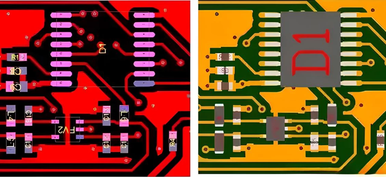
DFM matters because the cost of fixing a design problem scales directly with how late you catch it. Catching an issue at the schematic stage costs almost nothing. Catching it after a full prototype run costs weeks and thousands of dollars in respins, wasted material, and delayed market entry.
The Real Cost of Skipping DFM
PCB designs without DFM consideration typically produce first-pass assembly yields of 85–90%. DFM-optimized designs consistently reach 95–99% first-pass yield. That gap seems manageable on paper — until you are running a batch of 500 boards, at which point a 10% yield gap translates directly to scrap cost, rework labor, and delivery delay.
Here is how DFM affects the five variables that determine project profitability:
| Project Variable | Without DFM | With Professional DFM Integration |
|---|---|---|
| Prototype respins | 2–3+ rounds typical | 0–1 rounds; issues resolved before tape-out |
| Mass production yield | 85–90%, inconsistent | 95–99%, stable and reproducible |
| Cost control | Process and material frequently exceed budget | Process window locked during design phase |
| Time to market | Delays from design-manufacture handoff conflicts | Smoother prototype-to-production transition |
| Field return rate | Higher; late-stage fixes introduce new failure modes | Reduced through validated, locked DFM rules |
Why “Design Firm + Separate Factory” Is a Structural DFM Problem?
Many hardware teams use a design-only firm for schematics and layout, then engage a separate contract manufacturer for PCBA. This creates a structural gap: the design firm optimizes for electrical correctness; the factory optimizes for its own process window; nobody owns the interface between them.
This is where respins are born. The CM sends back a DFM issue report. The design firm interprets it differently from the factory. The client sits in the middle, paying for the delay and the debate.
A professional PCB design service that operates within the same technical system as a manufacturing partner eliminates this gap. DFM decisions happen in real time, with factory engineers and design engineers in the same conversation. At IWDF Solutions, our design team and PCBA manufacturing team share the same DFM rule library and participate in the same engineering review meetings — there is no handoff document traveling between two separate organizations with different incentives.
Understanding the business case for DFM is useful. But the practical question is: what does a DFM-integrated workflow actually look like, from the first client conversation through mass production?
How is DFM integrated step by Step?
DFM integration in a professional PCB design service runs across seven stages: manufacturing capability alignment, schematic and component selection, footprint review, layout with confirmed DFM rules, pre-prototype review, prototype feedback, and production handoff. Each stage has specific checkpoints and decision gates that prevent problems from carrying forward into the next phase.
Stage 1: Requirements and Manufacturing Capability Alignment
This stage happens before the first schematic net is drawn. The goal is to confirm that what the product needs to do can be built within the factory’s confirmed process window — and to make trade-off decisions before they become costly to reverse.
Key questions answered at this stage:
- What is the target application? (Industrial automation, IoT, EV charging, medical wearable, smart building?)
- What are the thermal, vibration, humidity, and shock environment requirements?
- What certifications are required? (CE, UL, FCC, ISO 13485 for medical devices, IATF 16949 for automotive?)
- What layer count, copper weight, and surface finish does the application need — and what is the cost impact of each option?
At IWDF Solutions, we provide clients with a written capability document at this stage. This lets the client evaluate engineering trade-offs at a business level. Choosing between a 6-layer and an 8-layer stack-up, for example, is not just a signal integrity decision — it is a cost and lead time decision that should be made with complete information before layout begins.
Stage 2: Schematic and Component Selection with DFM in Mind
Most DFM problems originate at the schematic level. Component choices made here — package type, BGA pitch, connector body size, footprint class — directly determine what the factory will encounter during assembly months later.
DFM-aware component selection includes:
- Avoiding EOL (end-of-life) or single-source components that create supply chain risk before the product reaches production
- Prioritizing package types with a proven SMT yield record — for example, a standard QFN over an exotic BTC variant where performance requirements allow the choice
- Annotating high-current and high-frequency nets at the schematic stage with a trace width floor, so the layout engineer does not start from a blank slate
- Confirming AOI and ICT detectability for critical devices before the BOM is locked
Stage 3: Footprint Creation and Library DFM Checks
A footprint error of 0.1 mm causes systemic assembly defects across an entire production run. This is one of the most underestimated risk points in the entire PCB design process.
All footprints at IWDF Solutions are built to IPC-7351 standards, which define land pattern geometry, courtyard clearance, and solder mask opening relative to assembly process class. Every new footprint goes through a CAM/DFM engineer review before it enters the production library. This step prevents a common and expensive failure: a PCB that assembles correctly in prototype quantities but develops consistent tombstoning, solder bridging, or component misalignment at production volumes because the footprint was designed for an ideal process rather than a real one.
Stage 4: Layout with DFM Rules Applied
Layout is where DFM rules become most visible. The design engineer works within a rule set confirmed against the factory’s actual process capability — not an assumed or default capability inherited from the layout tool’s library template.
| Rule Category | Typical Value | Why It Matters in Practice |
|---|---|---|
| Signal trace width | ≥ 4 mil (0.1 mm) | Margin against over-etch process variation |
| Trace-to-trace spacing (≤50V) | ≥ 4 mil (0.1 mm) | Prevents bridging; higher voltage requires wider clearance per IPC-2221 |
| Via drill diameter (PTH) | ≥ 0.3 mm | Below this, drill breakout risk rises significantly |
| Via annular ring | ≥ 0.1 mm after drill | Ensures thermal cycling and mechanical reliability |
| Solder mask bridge between pads | ≥ 0.1 mm | Prevents solder bridging during reflow and wave soldering |
| Copper to board edge | ≥ 0.3 mm (standard routing) | Prevents copper tear during panel depaneling |
| Aspect ratio (thickness ÷ drill Ø) | ≤ 8:1 | PTH copper plating long-term reliability |
Power routing follows a different logic entirely. Trace width on power nets is calculated from current load, copper weight, and allowed temperature rise — using IPC-2152 current capacity guidance as the starting point, not rule-of-thumb estimates. On industrial power boards, this calculation can be the difference between a board that runs stable at 10A continuous and one that fails field reliability testing at the six-month mark.
Stack-up design is finalized at this stage as well. The guiding principle is to use the fewest layers that satisfy signal integrity, power delivery, and EMC requirements. Every additional layer adds fabrication cost and lead time. DFM’s job is to reach the right layer count — not the minimum to save money or the maximum to avoid signal risk.
Stage 5: DFM Review Before Prototype Tape-Out
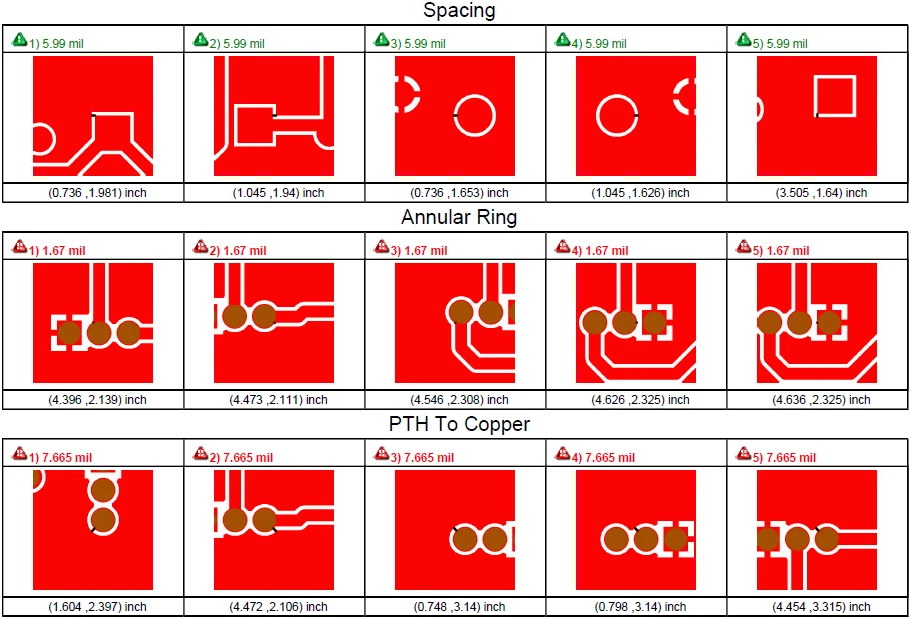
Before Gerbers are released to fabrication, a full DFM review runs against the final design using CAM tools and a factory-confirmed rule deck. The review checks for:
- Minimum annular ring violations at all via and pad locations
- Solder mask bridge conflicts between fine-pitch component pads
- Silkscreen-to-pad overlap, which causes confusion and errors at paste printing
- Missing or undersized test points for ICT and flying probe coverage
- Panel layout, tooling hole location, and fiducial placement for SMT line registration
- Controlled impedance trace identification and tolerance callout on the fabrication drawing
- Drill-to-copper and drill-to-board-edge clearance across all drill layers
This is not a software-only pass. Factory engineers from process, quality, and test review the output report alongside the design engineer. Issues are classified by severity: blocking (must fix before prototype release), major (strongly recommended to fix), and minor (acceptable risk with a documented waiver). The client receives the full report in English, with issue location references mapped to Gerber coordinates.
Stage 6: Prototype Build and DFM Refinement
The first prototype build is a structured data collection exercise — not just a proof of concept. Assembly staff document every anomaly observed during placement and reflow: bridging, tombstoning, paste insufficiency, component rotation errors. Test engineers log which nets failed ICT and the failure mode for each.
This data feeds directly back into the DFM rule set. A footprint that consistently causes tombstoning gets a pad geometry adjustment before production release. A via distribution pattern that contributes to board warpage gets redistributed in the next revision. Every change is made with documented rationale — not as an informal fix that nobody records and nobody can trace later.
Stage 7: Scaling to Mass Production with Locked DFM Rules
Once prototype-level DFM issues are resolved, the validated rule set for that product — confirmed process window, approved BOM, panel design, test coverage requirements — is locked as the production baseline.
For repeat clients at IWDF Solutions, we maintain a project-specific DFM rule file for each hardware platform. When a new revision or a derivative product starts, our engineers load this rule file into the CAD environment before any routing begins. This ensures that every new design iteration benefits from the manufacturability knowledge gained in earlier builds, instead of repeating the same mistakes.
For long‑term partners, we also maintain approved alternate components and pre‑qualified PCB stack‑ups. This reduces sourcing risk and shortens the time needed to qualify new designs for volume production, especially when component availability or global logistics change.

Practical DFM Guidelines PCB Buyers Should Know?
If you source PCB design and manufacturing from overseas, you carry extra risk in quality, schedule, and communication. The good news is that many of these risks are controllable if you use DFM as a decision tool.
As an overseas buyer, you should focus on two things: confirm the manufacturing capability of your potential partner against the needs of your design, and prepare your design data in a way that allows engineers to run a meaningful DFM review instead of guessing your intent. This section gives you simple, concrete checklists for both.
Key Manufacturing Capabilities to Confirm
Before you share any files, ask your potential partner for a written capability summary. At a minimum, verify these points:
- Minimum trace width and spacing for standard and HDI processes
- Minimum mechanical drill size and microvia capabilities
- Maximum layer count supported with stable yield
- Available copper weights and how spacing rules change with each copper weight
- Supported board thickness range and maximum drill aspect ratio
- Available surface finishes and typical lead times for each
- Impedance control capability and tolerance (for differential pairs and RF)
- Minimum solder mask bridge width and registration tolerance
If the factory cannot provide this in a clear document, you will likely face surprises later. A mature Shenzhen manufacturer should have this ready in English and be prepared to answer clarifying questions.
How to Prepare Design Files for a DFM Review
When you ask for a DFM review, the quality of the feedback depends heavily on the quality of the data you provide. For a practical, engineer‑friendly DFM review, include:
- Gerber or ODB++ data for all layers
- Full BOM with manufacturer part numbers and package descriptions
- Pick‑and‑place (centroid) file for assembly
- Fabrication drawing with stack‑up, tolerances, and special process notes
- Assembly drawing showing critical orientations, polarities, and mechanical constraints
- Short design requirement brief (environment, lifetime, certifications, current/voltage range)
Here is a concise checklist you can use internally or send to your team:
| Item | Description | Why It Matters |
|---|---|---|
| Capability sheet | Written document from factory | Confirms if your design is buildable without heavy compromise |
| Complete BOM | With MPNs and package details | Enables DFA review, sourcing checks, and alternates planning |
| Gerber/ODB++ | Full board definition | Required for any serious DFM or CAM analysis |
| Fab/assy drawings | Notes, stack‑up, and markings | Prevents misinterpretation at production |
| Requirements brief | Environment and compliance targets | Guides material choice and test strategy |
Pre‑Design DFM Checklist for Overseas Buyers
To make this practical, here is a “Pre‑design DFM Checklist for Overseas PCB Buyers” you can copy and adapt:
- Confirm your target application and environment (industrial, medical, automotive, consumer).
- Get a written capability sheet from at least two potential PCB partners.
- Decide on your target layer count range before layout starts.
- Clarify if your design will require controlled impedance or RF‑related constraints.
- Check if any key components are at risk of EOL or allocation.
- Decide up front which tests you expect: ICT, flying probe, functional test.
- Ask for a sample DFM report from each potential supplier.
- Align on NDA and IP‑protection measures before sharing full design files.
- Agree on who owns design changes if DFM issues are found (you vs. supplier).
- Set clear timelines for DFM feedback and design update cycles.
You can easily turn this checklist into a one‑page PDF or screenshot that your internal team uses every time they start a new project with a China‑based supplier.
Using DFM to Manage Supplier Risk
DFM is also a powerful way to compare and manage suppliers. When you shortlist two or three professional PCB design services in China or Shenzhen, give them the same limited design sample (for example, one section of your board) and ask for a DFM review. Compare:
- How specific their feedback is
- Whether they flag real manufacturing risks rather than only cosmetic issues
- How do they balance cost, risk, and performance in their suggestions
- Whether they propose alternative stack‑ups, processes, or component packages
A supplier who gives you thoughtful DFM feedback on a small test project will likely be a better long‑term partner than one who simply says “OK, we can make it” and sends a quote.
How to Evaluate a PCB Design Partner’s DFM Capability?
By this point, you know that “we also do DFM” is not enough. You need a way to separate marketing claims from real, repeatable engineering practice.
The simplest way to evaluate a potential PCB design partner is to ask concrete questions, request specific documents, and observe how they respond when you give them a small, low‑risk test task.
Questions You Should Always Ask
Use these questions in your first technical call or email:
- Can you share your standard DFM guidelines and manufacturing capability document?
- Do your DFM engineers get involved from the schematic/layout stage, or only just before production?
- How do you deliver DFM feedback: as a formal report with issue locations and severities, or as general comments?
- Who is responsible for implementing DFM‑driven design changes on your side?
- How quickly do you typically return a DFM report on a new design?
The answers do not need to be perfect, but they must be concrete. Vague responses usually indicate that there is no real DFM process behind the marketing.
Documents and Processes You Should Expect
A professional DFM‑driven service should be able to provide:
- A current capability and design guideline document.
- A sample DFM report (with client information removed) showing how they mark issues.
- An example of meeting notes or summary emails from an engineering review.
- A clear description of their version control and change approval process.
Here is a simple table you can use when you compare suppliers:
| Item | Weak Signal | Strong Signal |
|---|---|---|
| Capability document | “We will just fix it.” | Detailed table with clear limits and notes |
| DFM report | Short email, no locations or severities | Structured report with coordinates, screenshots, and priorities |
| Change process | Only sales respond | Clear flow for approval, ECO tracking, and version control |
| Communication | Only sales responds | Access to English‑speaking engineers and PM |
What You Can Expect from IWDF Solutions
From our side, you can expect:
- A detailed, English‑language capability document for PCB design and manufacturing in Shenzhen.
- DFM engineers are involved from schematic through layout and into production support.
- Formal DFM reports with screenshots, coordinates, and severity tags.
- Protected handling of your design data under NDA, with access control and secure transmission.
- A project manager who follows your job from the first call to mass production, ensuring that DFM decisions are implemented and verified.
If you already have schematics or Gerber files, you can send them to us for DFM check. We will return manufacturability feedback and practical suggestions within an agreed number of working days, depending on the complexity of your board.
FAQ About DFM and PCB Design Services
What is the difference between DFM and standard PCB design checks?
Standard PCB design checks focus on electrical rules and basic layout constraints. DFM checks go further and evaluate whether the design can be fabricated, assembled, and tested reliably on real equipment with acceptable yield and cost.
At which stage should DFM be applied in a PCB project?
DFM should start at the requirements and schematic stages, not at the end of layout. Early DFM involvement helps you choose the right packages, stack‑up, and rules so you avoid painful redesigns later.
Can DFM really reduce PCB manufacturing cost for small batches?
Yes. Even in small batches, DFM helps you avoid extra layers, unnecessary special processes, and hard‑to‑source components. This keeps unit cost and NRE under control and reduces the risk of rework.
How does DFM help when working with a China‑based PCB factory?
DFM bridges the gap between your design assumptions and the factory’s real capabilities. A good DFM process at a China or Shenzhen factory can catch misalignments early, reduce miscommunication, and make your first run far more predictable.
What files do I need to send for a DFM review?
For a useful DFM review, send your Gerber or ODB++ data, BOM with manufacturer part numbers, pick‑and‑place file, and any fabrication and assembly drawings you have. Also include a short description of the application and any special requirements.

