

Understanding the Challenge Behind Multi-Layer PCB Reverse Engineering
Reverse engineering a multi-layer PCB is significantly more demanding than dealing with single or double-layer boards. These complex structures—often with four, six, or even more conductive layers—are compact, densely populated, and frequently use buried or blind vias, making inner connections virtually invisible without advanced techniques. For hardware engineers, especially in failure analysis, legacy recovery, or competitive benchmarking, knowing how to reverse engineer such PCBs is an essential skill.
How to Reverse Engineer a Multi-Layer PCB?
To reverse engineer a multi-layer PCB, document the board with high-resolution images, identify components and layer structure, remove solder masks if needed, and scan or photograph each layer after safe delayering. Use CAD software to redraw the schematic and PCB layout, verifying connections with measurement tools. Always document each step for accuracy and legal compliance.

Step-by-Step Guide to Reverse Engineering a Multi-Layer PCB
Step 1: Initial Visual Inspection & Documentation
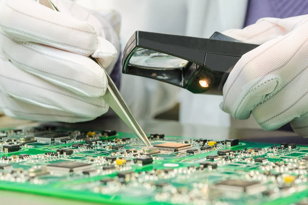
Before you touch the soldering iron or start peeling away layers, begin with a full visual inspection.
- Lighting & Magnification – Use a bright, diffuse light source and a stereo microscope to examine both sides. Look for reference designators (R1, C5, U2, etc.), test points, and manufacturing markings.
- Photography – Take high-resolution photos of both sides, ensuring scale consistency (place a ruler in the frame). Capture the edges, which often reveal the layer stack-up.
- Board Condition – Note any corrosion, rework marks, or damaged pads. These can affect reverse engineering accuracy.
- Label Everything – Assign internal IDs to the board and its components before proceeding. This is essential if you’re documenting multiple boards.
Pro tip: Even if you later delayer the PCB destructively, good documentation allows you to digitally “rebuild” the original in CAD without needing another sample.
Step 2: Identify Components and Markings
This step is where you start building the component database for the schematic.
- Component ID – Using your photos, label each component according to its reference designator.
- Part Number Lookup – Use tools like Octopart, Digi-Key, or manufacturer datasheets to identify exact models.
- Package Measurement – Calipers are useful for confirming footprint sizes if the part number is unreadable.
- Marking Codes – For ICs, note down every marking — even partial — and cross-reference with IC marking code databases.
- Orientation – Mark pin 1 orientation for ICs, polarity for diodes, and capacitor polarity.
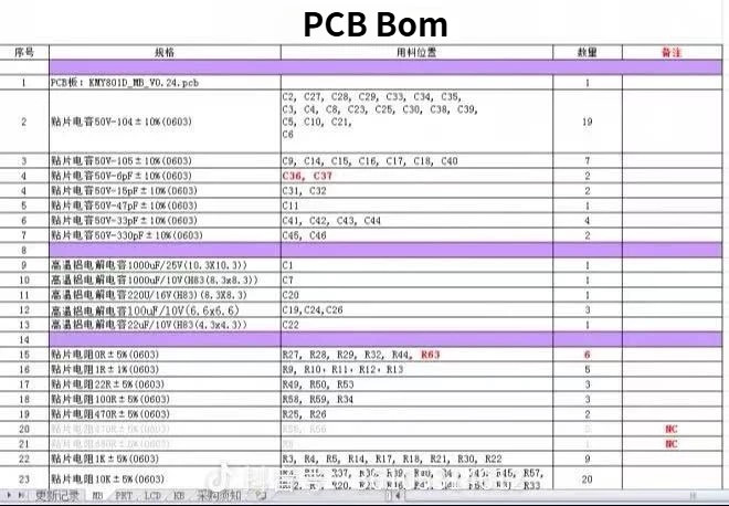
- Pre-Disassembly Recording – Carefully document each component’s location, orientation, package models, identifying labels, and quantities before taking the device apart. Take comprehensive photos and compile a BOM
Beginner tip: Many beginner reverse engineers skip accurate part ID, but without it, you risk creating a schematic that’s electrically correct but functionally wrong.
Step 3: Determine the Number of Layers and Stack-Up
Knowing the exact layer count is essential before deciding on a reverse engineering method.
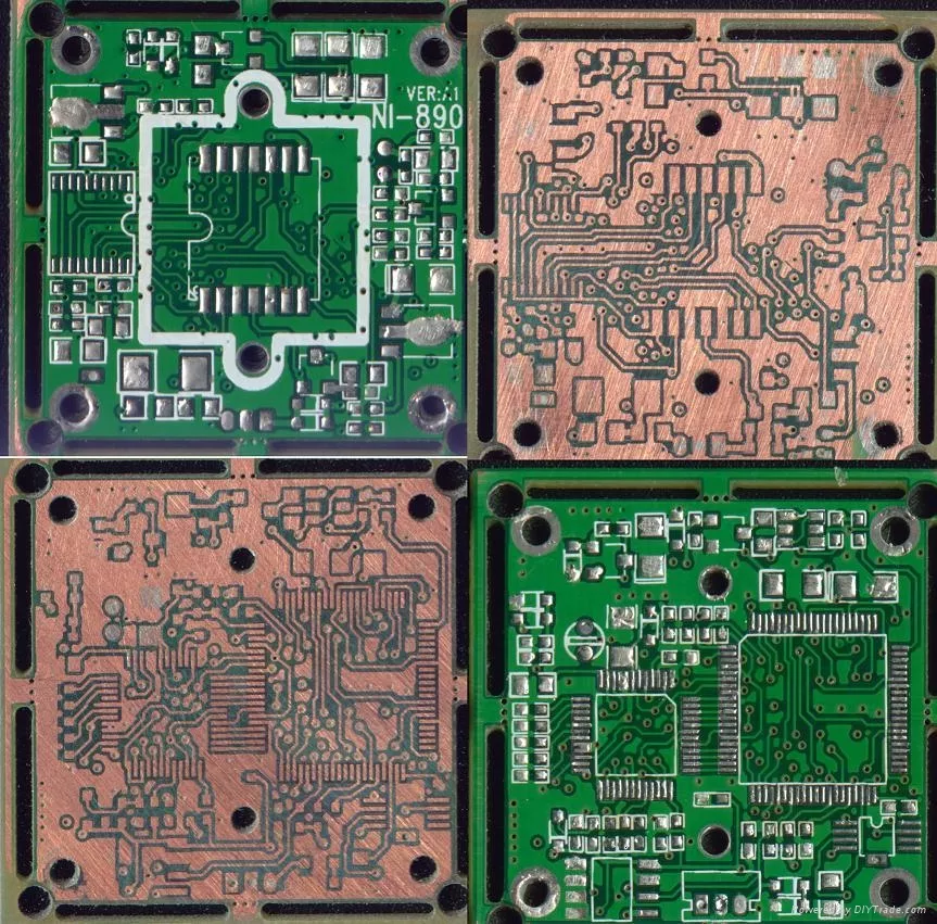
- Edge Inspection – Examine the board edge under a microscope. You can often see faint copper lines between fiberglass layers. Count them to estimate the layer number.
- X-ray Imaging (if available) – This reveals hidden vias and internal traces without damaging the board.
- Manufacturer Clues – Check for silkscreen text like “4L” or “6L,” indicating layer count.
- Stack-Up Guessing – In typical designs:
- 4-layer PCB – Top signal, ground plane, power plane, bottom signal
- 6-layer PCB – Top signal, ground, internal signal, power, internal signal, bottom signal
Safety note: If you’re working on a high-voltage board, always discharge capacitors before handling. Even powered off, they can hold a dangerous charge.
Step 4: Remove Components for Clearer Traces
For accurate reverse engineering — especially when scanning or imaging traces — it’s often necessary to remove at least some components.
Why remove components?
- To expose hidden pads and trace starts/ends.
- To allow uninterrupted imaging of solder pads.
- To simplify schematic reconstruction.
Tools & Techniques:
- Desoldering Station: Hakko FR-301 or Quick 861DW for hot-air rework.
- Solder Wick: Chemtronics Soder-Wick for pad cleanup.
- Flux: Amtech NC-559 or Kester 951 for better heat transfer and less oxidation.
- Tweezers: ESD-safe, precision tips (Vetus ESD-15) to avoid damaging pads.
Tips for Beginners:
- Work at the lowest possible hot air temperature to avoid delaminating the PCB.
- Use Kapton tape to shield components you’re not removing.
- Always store removed parts in labeled anti-static bags.
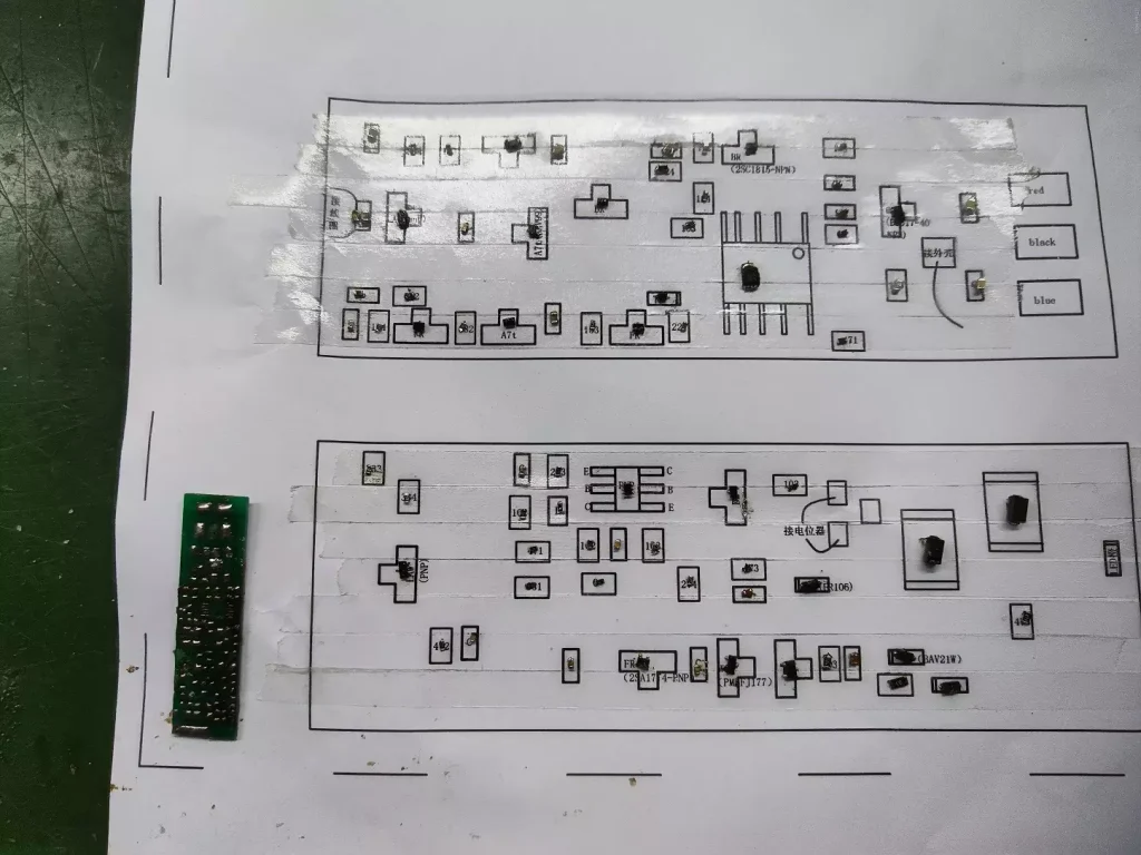
Step 5: Photographing & Scanning All Layers
Once components are removed (or at least the obstructive ones), you can capture detailed images.
Photography Method:
- Use a DSLR or mirrorless camera with a macro lens (Canon EOS R + RF 100mm macro is excellent).
- Mount the board on a flat, well-lit surface with diffuse LED lighting to reduce glare.
- Keep the camera perfectly perpendicular to avoid distortion.
Scanning Method:
- Flatbed scanners like Epson Perfection V39 or V600 can give high-resolution images (1200–2400 dpi).
- Scan both top and bottom layers with a calibration ruler in-frame for scaling in CAD software.
Pro Imaging Tip: Take multiple angles of each layer. Sometimes glare or reflection will hide faint traces, and having alternative angles can help during CAD reconstruction.
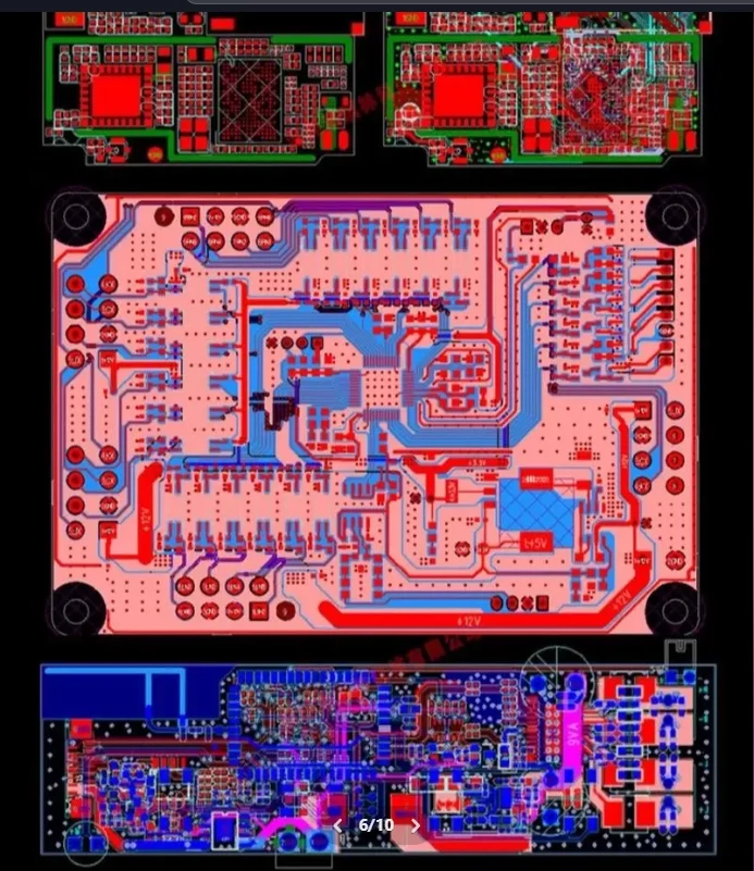
Step 6: Safe Delayering Methods (Non-Destructive vs Destructive)
Multi-layer boards hide most of their connections in inner copper planes. To see them, you need to remove material layer by layer — but this must be done carefully.
Non-Destructive Methods:
- X-Ray Imaging: Tools like the DAGE X-ray system can reveal internal traces without touching the board.
- CT Scanning: Advanced, expensive, but offers full 3D internal mapping. Used by companies like PCBHero or ScanCAD.
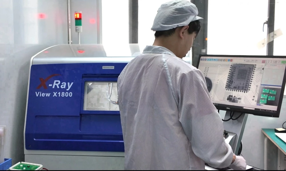
Destructive Methods:
If non-destructive tools aren’t available, mechanical or chemical delayering is the next option.
- Mechanical Grinding: Use a precision PCB grinder like the ProtoLaser LDI or handheld systems like the MetPrep SiC grinder. Sand away fiberglass layer by layer until the copper is exposed.
- Chemical Etching: Ferric chloride or ammonium persulfate can remove copper selectively, but requires strict PPE use.
Safety Precautions:
- Always wear a respirator (3M 6200 with P100 filters) when grinding fiberglass — inhaling it can cause lung damage.
- Use gloves, goggles, and a fume extractor when using chemicals.
- Work in a well-ventilated area.
Beginner Advice: Start with a scrap PCB to practice delayering before working on your actual target board — mistakes here are irreversible.
Step 7: Tracing & Mapping Connections
Once all layers are imaged or exposed, it’s time to digitally map every trace.
Process:
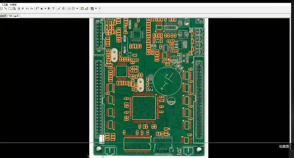
- Import Images into CAD – Load your scans into a program like KiCad, Altium Designer, or EasyEDA.
- Align & Scale – Use calibration rulers in your images to set exact scale in CAD. Align top/bottom layers precisely.
- Trace Drawing – Manually draw each track using the photo as a reference. Keep separate layers for each PCB layer in the CAD file.
- Via Mapping – Mark all vias and note which layers they connect. For multi-layer boards, this is where X-ray images pay off.
Pro Tip: Use a color-coded system for each layer in CAD. This makes it easier to track nets later when creating the schematic.
Step 8: Reconstructing the Schematic in CAD
With all connections mapped, you can now rebuild the circuit.
Steps:
- Netlist Extraction – From your traced layout, generate a netlist file.
- Component Placement – Place the identified components in the schematic view.
- Wiring – Connect components based on the traced nets.
- Electrical Rule Check (ERC) – CAD software will warn if there are short circuits, open nets, or missing connections.
Software Recommendations:
- KiCad – Free, open-source, supports multi-layer boards.
- Altium Designer – Industry-standard, excellent for complex boards.
- OrCAD Capture – Preferred for high-speed or dense layouts.
Beginner Advice: Don’t expect your schematic to look exactly like the original designer’s — your goal is functional equivalence, not cosmetic replication.
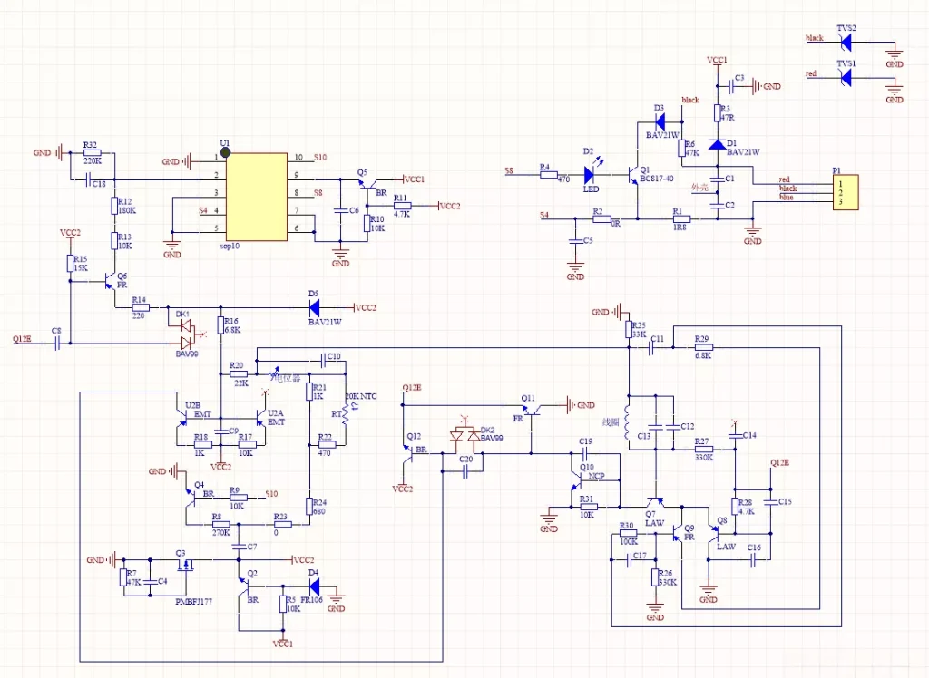
Step 9: Recreating the PCB Layout
Once you have the schematic, you can rebuild the PCB layout if needed.
Why This Step Matters:
- To create a fully functional duplicate PCB.
- To modify or upgrade the design for your own use.
Process:
- Import Schematic – Into your PCB CAD tool.
- Layer Stack Definition – Match the original stack-up you identified earlier.
- Component Placement – Position components as close to original locations as possible.
- Routing – Follow your traced paths. Use differential pairs and impedance control for high-speed signals if applicable.

Step 10: Validation with Electrical Testing
No reverse engineering is complete without testing.
Tools Needed:
- Multimeter: Fluke 87V for continuity and resistance checks.
- Oscilloscope: Rigol DS1054Z or Siglent SDS1104X-E for signal testing.
- Power Supply: Korad KA3005P with current limiting to prevent damage.
Testing Steps:
- Continuity Test – Check all nets for proper connections.
- Power-Up Test – Start with a current limit and gradually increase voltage.
- Functional Test – Compare signals at key test points against known working boards or datasheet specs.
Layer Visualization Example
Here’s how a typical 4-layer PCB stack-up looks:
Layer 1 – Top signal (components + traces)
Layer 2 – Ground plane
Layer 3 – Power plane
Layer 4 – Bottom signal
For a 6-layer PCB, the stack might be:
Layer 1 – Top signal
Layer 2 – Ground plane
Layer 3 – Internal signal
Layer 4 – Power plane
Layer 5 – Internal signal
Layer 6 – Bottom signal
Visualization Tip: In CAD, use bright contrasting colors (red, green, blue, yellow, purple, orange) for each layer to make them easier to distinguish during tracing.
Safety Precautions in PCB Reverse Engineering
- Electrical Safety: Always discharge capacitors before handling boards.
- Chemical Safety: Handle etchants in a fume hood or outdoors with gloves and goggles.
- Mechanical Safety: Wear a respirator when sanding fiberglass layers.
- Legal Safety: Ensure you are reverse engineering for educational, repair, or authorized duplication purposes to avoid intellectual property violations.
Common Mistakes to Avoid in PCB Reverse Engineering
- Skipping Documentation Before Disassembly
Beginners often start pulling components without photographing or labeling them first. This can make it impossible to accurately reconstruct the original design. - Not Identifying Components Accurately
Guessing component values or types instead of verifying through datasheets can lead to a schematic that “works on paper” but fails in real life. - Overheating Pads During Desoldering
Excessive heat can lift pads or damage internal vias. Always use temperature-controlled tools. - Failing to Recognize Multi-Layer Complexity
Treating a 6-layer PCB like a simple 2-layer can cause you to miss hidden power/ground planes and internal signal routes. - Ignoring Legal Restrictions
Reverse engineering for commercial duplication without authorization can violate patents, copyrights, or trade secrets.
Best PCB Reverse Engineering Software & Tools
CAD Software
- KiCad – Open-source, multi-layer support, great for beginners and pros.
- Altium Designer – Premium, used by industry professionals for complex designs.
- OrCAD Capture & Layout – Excellent for high-speed boards and simulation integration.
Imaging Tools
- Epson Perfection V600 Scanner – High-resolution scanning for PCB layers.
- Canon EOS R + 100mm Macro Lens – Professional-grade board photography.
- DAGE X-ray Inspection Systems – For non-destructive internal trace imaging.
Reverse Engineering Utilities
- ScanCAD ScanFAB – Automated layer reconstruction from scans.
- ZofzPCB Viewer – 3D Gerber file viewer for verification.
- Netlist Extractors – Built into most CAD tools for schematic generation.

Legal and Ethical Boundaries in PCB Reverse Engineering
One of the most misunderstood aspects of PCB reverse engineering—especially in multi-layer boards used in commercial products—is its legal framework. Reverse engineering itself is generally legal in many jurisdictions, particularly when conducted for interoperability, education, repair, or failure analysis. However, complications arise if the board incorporates patented technologies or copyrighted layouts.
Trade secret law in most countries allows reverse engineering as long as the original product was lawfully acquired and the information wasn’t obtained through breach of contract or confidentiality. However, patent protection can limit reuse or commercial replication. In short, while learning from a multi-layer board is fair game, cloning it and selling the product may infringe rights.
To ensure ethical compliance:
- Avoid distributing reverse-engineered schematics if the board is protected by IP.
- Use the analysis strictly for internal development or restoration.
- Document the ownership of the original board and the purpose of reverse engineering.
If in doubt, consult a legal advisor familiar with IP laws in your region or industry.
From Layers to Functionality: Interpreting the Circuit Behavior
Multi-layer PCBs are often designed for performance—not just layout compactness. As such, reverse engineering shouldn’t just recreate connections, but reveal why the board was designed that way.
Take, for example, a six-layer board used in a communications device. Two internal layers may be entirely dedicated to ground and power planes, not for routing. These layers serve critical roles in signal integrity, EMI reduction, and return path consistency. A surface inspection might miss these altogether unless the reverse engineer recognizes power distribution decoupling patterns, bypass capacitor placements, and via stitching techniques.
Reconstructing the functional architecture means observing not just how traces connect, but how subsystems interact. Isolating the analog front-end from the digital logic, identifying power sequencing circuits, or discovering protected GPIOs can give immense insight into design intent. This is what separates basic replication from informed reverse engineering.
When to Use a PCB Reverse Engineering Service?
Reverse engineering a multi-layer PCB by hand is time-consuming and often technically limited by imaging capabilities. That’s where professional PCB scanning services come in. These services use industrial-grade X-ray tomography, laser ablation, or even chemical delamination techniques to expose each layer with micron-level precision.
Use a service when:
- The PCB has more than 4 layers, and internal vias are tightly nested.
- High-resolution inner layer mapping is critical (e.g., in high-frequency or RF designs).
- Time and cost constraints make manual grinding or image tracing impractical.
Be sure the vendor respects client confidentiality, especially if the board includes proprietary or regulated technology. Many reputable platforms like ScanCAD, PCBTok, and others offer secure handling and non-disclosure guarantees.
Some services even return Gerber files and a partially reconstructed netlist, saving engineers weeks of manual labor.

Practical Considerations and Reverse Engineering Tips
- Always start with the easy wins. Map out all through-hole components, visible nets, and silkscreen markings before diving into inner layers.
- Use known IC pinouts to predict invisible routing. Microcontroller datasheets are invaluable—knowing VCC, GND, CLK, or I/O pins lets you infer net groupings.
- Watch out for differential pairs and impedance-controlled traces, especially in high-speed designs. These traces often run symmetrically on internal layers and can reveal clock or data buses.
- Reconstruct schematic blocks, not the entire netlist at once. Identify power management, memory interface, and signal conditioning blocks separately, then tie them together logically.
- Document every decision—why a net is assigned, why a component is interpreted as a regulator, etc. Reverse engineering is just as much about rational deduction as it is about observation.
Case Study: Rebuilding a 6-Layer Industrial Controller
To illustrate the process, let’s walk through a simplified case. A client brought in an industrial controller board that was no longer in production, but essential for legacy system operation. The board had no schematics, only one defective unit.
After capturing macro photographs and scanning the outer layers, we confirmed it was a 6-layer PCB, with blind and buried vias. The main MCU was a 144-pin STM32F4, and an FPGA (Lattice ICE40) occupied the lower right corner.
Using X-ray imaging, we traced inner power and ground planes. Signals running from the FPGA to external connectors were routed internally, requiring advanced image processing to distinguish them from stitched vias.
With datasheets in hand and experience on similar designs, we reconstructed the following:
- Dual 3.3V and 1.2V rails for logic power
- SPI and JTAG routing between the MCU and the FPGA
- Isolated RS-485 transceiver for fieldbus protocol
Finally, we redrew the schematics in KiCad, validated pin mappings using logic probing on the working board, and produced a netlist accurate enough to build replacement units.
Summary: Reverse Engineering as a Skill, Not a Shortcut
Reverse engineering a multi-layer PCB demands precision, patience, and the right methodology. From initial inspection to schematic reconstruction and final validation, every step builds a clearer picture of the circuit’s inner workings. By using proper tools, following safety protocols, and respecting legal limits, you can turn a mystery PCB into a fully documented design — and sharpen your electronics skills in the process.
Looking for a hassle-free way to go from reverse engineering to a fully manufactured PCB?
IWDF Solutions offer a one-stop solution — from detailed circuit analysis to professional PCB fabrication — so you can bring your project to life faster and with confidence. Submit your inquiry today and let’s make it happen.
FAQs
Q1. What industries most often require multi-layer PCB reverse engineering?
Multi-layer PCB reverse engineering is widely applied in aerospace, medical devices, automotive electronics, and industrial automation. In these fields, replacing damaged hardware with brand-new equipment can be extremely costly and time-consuming. Reverse engineering offers a faster and more economical alternative, allowing critical systems to remain operational without long procurement delays.
Q2. Can multi-layer PCB reverse engineering help with failure analysis?
Yes. By exposing internal layers and mapping connections, engineers can identify design flaws, heat-stressed vias, or short circuits that are invisible from the outside. This process is particularly valuable when diagnosing recurring field failures.
Q3. How does signal integrity affect reverse engineering of multi-layer boards?
Signal integrity is crucial in high-speed designs. Reverse engineers must pay attention to controlled impedance traces, differential pairs, and reference planes. Understanding these helps reconstruct the original design intent and prevents misinterpretation of routing strategies.
Q4. Is it possible to reverse engineer HDI (High-Density Interconnect) PCBs?
HDI boards, with microvias and ultra-thin dielectric layers, are among the hardest to reverse engineer. Advanced X-ray tomography or laser ablation tools are often required. While possible, the cost and effort are significantly higher compared to standard multilayer PCBs.
Q5. What role does 3D scanning play in PCB reverse engineering?
3D scanning, combined with CT imaging, allows engineers to visualize the entire PCB stack in volumetric detail. Unlike 2D X-ray, 3D methods provide clearer separation of overlapping traces and vias, improving accuracy in reconstructing dense multilayer designs.
Q6. Can reverse engineering a PCB reveal its manufacturing quality?
Yes. By analyzing copper trace width, via plating, and lamination consistency across layers, engineers can evaluate the quality of the board’s original manufacturing process. This insight helps when selecting replacement vendors or diagnosing product lifespan issues.
Q7. What are the cost factors in multi-layer PCB reverse engineering?
The cost depends on the number of layers, required precision, and chosen method (manual, destructive, or service-based). A simple 4-layer board might be analyzed in-house with minimal equipment, while a 12-layer high-speed PCB could require specialized service costing thousands of dollars.
Q8. Can reverse engineering recover firmware or embedded code?
No. PCB reverse engineering reveals hardware connections but does not extract microcontroller or FPGA firmware. Accessing embedded code requires separate techniques such as JTAG, SWD debugging, or chip-off analysis, which often involve additional legal considerations.
Q9. What future technologies may simplify PCB reverse engineering?
Emerging AI-powered image recognition, automated EDA reconstruction, and high-resolution CT scanning are expected to significantly reduce manual tracing effort. These tools could transform reverse engineering into a faster, semi-automated process over the next decade.

