

A multilayer PCB is a circuit board with three or more conductive copper layers, built to support high-density, high-performance electronics in compact form factors. The board is constructed by laminating alternating signal, power, and ground layers using core and prepreg materials, with vias—through-hole, blind, or buried—connecting the layers as needed. Multilayer PCB design factors include a balanced stack-up to prevent warping, controlled impedance for signal integrity, effective thermal management through copper planes and vias, and strategic ground/power placement to reduce EMI and noise.

Multilayer vs. Single / Double-Sided PCBs
| Feature | Double-Sided PCB | Multilayer PCB (4–8 layers) |
|---|---|---|
| Layer Count | 2 copper layers (top and bottom) | 4–8+ copper layers, including internal planes |
| Routing Density | Limited; requires many vias and tight spacing | High; internal layers provide additional routing space |
| Signal Integrity | Poor for high-speed signals; reference planes are fragmented | Excellent; continuous ground/power planes control impedance |
| EMC Performance | Difficult to meet emissions standards | Easier to achieve compliance with proper plane design |
| Power Distribution | Power traces act as antennas; high inductance | Dedicated power planes provide low-impedance distribution |
| Design Complexity | Low to moderate | Moderate to high; requires careful stack-up planning |
| Prototype Cost | Lower | Higher (roughly 2–4× for 4-layer vs. 2-layer) |
| Mass Production Cost | Economical for simple designs | Cost-effective when density or performance justifies it |
Key takeaway: More layers do not automatically mean a better board. The goal is to use the minimum number of layers that meet your electrical, mechanical, and reliability requirements while staying within budget.

When to Choose a Multilayer PCB?
A multilayer circuit board is not always the right first answer. It becomes the right answer when your product has constraints that fight each other. Here are common triggers that justify moving to a multilayer PCB:
- You have high-pin-count parts, like fine-pitch BGAs, and you cannot escape and route on two layers.
- You have many parts and the top and bottom layers will be too crowded.
- You have high-speed interfaces (USB 3.x, PCIe, DDR, MIPI, LVDS, Ethernet) and you need controlled impedance and stable reference planes.
- You have strict EMI limits, and you need solid ground planes to control return paths and reduce radiation.
- You have fast signals, tight EMC goals, or sensitive analog blocks that need clean reference planes.
- You need better power integrity, with low impedance power distribution and short current loops.
- You have mixed-signal blocks (RF + digital + sensitive analog) and you need real isolation by structure, not only by spacing.
- Your board has high power density, and you need copper planes and thermal vias to move heat.
- You have mechanical limits, and you must reduce board size and connector count while keeping function.
Step-by-step multilayer PCB design workflow
This is a practical multilayer PCB design tutorial you can follow on real projects. Use it as a checklist and also as a way to judge a multilayer PCB design services provider.
Step 1: Requirements and constraints
Your requirements decide whether you need internal planes, controlled impedance, and advanced interconnect (blind/buried vias, microvias, via-in-pad). Those features are the main reasons engineers move from 2-layer to multilayer in the first place. Requirements also decide whether you can stay on “standard” stack-ups or you must use special materials, tighter thickness control, or HDI build-ups.
In multilayer boards, early choices lock cost and physics. If you do not define speed, noise limits, current, size, and compliance targets now, you will pick the wrong layer count and stack-up. Then you will redo fanout, impedance work, and routing later, which is the most expensive kind of rework.
Include (keep it simple and specific):
- Electrical: main interfaces, edge rates (or data rates), and which nets are sensitive.
- Power: rails, peak current, allowed ripple, and any fast load steps.
- EMC: what cables connect, what emissions limits exist, and what parts must stay quiet.
- Mechanical: outline, keepouts, mounting holes, height limits, and connector locations.
- Cost and schedule: target layer count options and expected volumes.
Practical tip: ask your manufacturer for their standard stack-ups early. This saves time and avoids custom builds that cost more and carry more risk.

Step 2: Stack-up planning (this decides most outcomes)
Stack-up is the “core” multilayer decision. It defines plane locations, dielectric thickness, coupling between layers, and mechanical symmetry. It also decides which layers can carry controlled-impedance traces and how clean your return paths can be.
You cannot set correct impedance rules, pick via spans, or make good plane decisions without a real stack-up. If you start placement and routing without it, you often discover later that trace widths do not fit, plane layers are missing, or the board warps because the build is not balanced.
A symmetric stack-up is a key goal because asymmetric builds create uneven stress during lamination, which increases bow and twist risk. Designers also tend to prefer even layer counts, because odd layer counts are more likely to cause warping problems and often do not save as much cost as people hope.
Why symmetry matters (multilayer reason):
- A symmetric stack-up helps balance stress in lamination and soldering.
- It reduces bow and twist risk.
- It makes results more repeatable across batches.
In practice, symmetry means:
- The layer types are mirrored around the center of the board.
- Dielectric thickness is balanced top-to-bottom.
- Copper distribution is kept as even as possible between paired layers.
Common layer-count choices (why engineers do this):
Most teams start with 4, 6, or 8 layers because those counts let you dedicate at least one solid ground plane (often more), which is the foundation for SI/EMI control in multilayer designs.
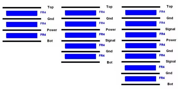
Table: Common stack-up templates (starting points)
| Board type | Typical stack-up idea | Best for | Notes |
|---|---|---|---|
| 4-layer multilayer PCB | Signal / GND / PWR / Signal | Moderate speed, moderate density | Good baseline, but routing can still get tight. |
| 6-layer multilayer circuit board | Signal / GND / Signal / Signal / PWR / Signal (or Signal / GND / Signal / PWR / GND / Signal) | Higher density and cleaner EMI | More flexibility for SI/PI and placement. |
| 8-layer multilayer circuit boards | Signal / GND / Signal / PWR / GND / Signal / GND(or PWR) / Signal | Very dense and tougher EMC | Plane integrity and symmetry become even more important. |

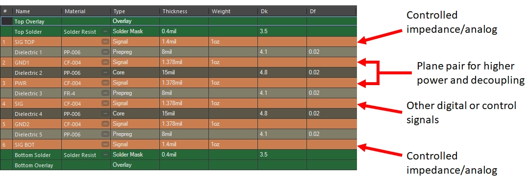
A clear 6-layer example you can copy (and why it helps):
This example puts a solid ground plane right under the top layer. That supports controlled impedance and a clean return path for high-speed nets. It also reserves internal layers for routing density.
Example 6-layer stack-up for controlled impedance and solid return paths:
- L1 Top: High-speed signal + short local routes
- L2: Solid GND plane (main reference for L1)
- L3: Signal (internal)
- L4: Signal (internal, route perpendicular to L3 when possible)
- L5: Power plane (or carefully managed split power)
- L6 Bottom: Signal + connectors and low-speed routes
Practical tip: if you use split power planes, plan them early and set routing rules so fast signals never cross a split.
Step 3: Impedance and return-path strategy
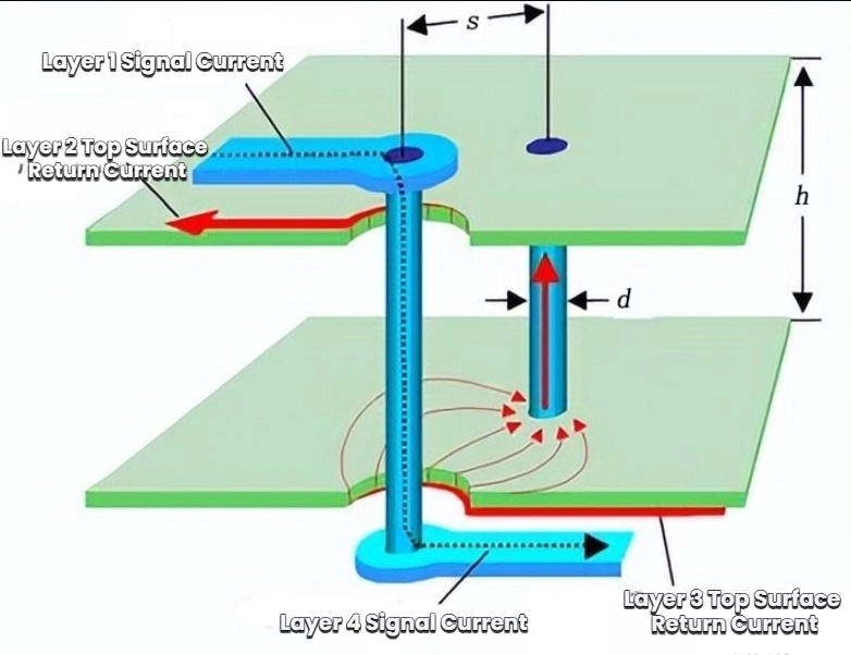
Return paths are a plane problem, and planes are a multilayer feature. This step converts your stack-up into electrical rules: which layer a net must stay on, which plane it references, and what is forbidden (like crossing plane splits). This is one of the most “multilayer-only” parts of the whole workflow.
Impedance depends on the geometry that is defined by the stack-up: trace-to-plane spacing and dielectric choice. Return path depends on where the planes are and whether they are continuous. So this must come after Step 2 and before via planning, placement, and routing.
Controlled impedance depends on the full geometry. Trace width is only one part. The distance to the reference plane and the dielectric also matter.
Use these rules (and why they matter in multilayer):
- Put fast signals on layers that have a solid ground plane right next to them (keeps fields contained, improves predictability).
- Keep return paths continuous along the whole route (avoids large loops and EMI).
- When signals change layers, add nearby stitching vias so the return current has a clear path (prevents return-path “detours”).
- Avoid routing fast signals over split planes (prevents broken reference and noise spikes).
Service-provider test: if a provider is serious about SI/EMI, they ask for impedance targets and they align them with a build your chosen fabricator can produce.
Step 4: Via strategy (through, blind, buried, microvia, via-in-pad)
Vias are the “vertical wiring” of multilayer PCBs. The via type you choose changes routing density, plane integrity, and manufacturability. Blind/buried vias and microvias are not generic PCB features. They are multilayer/HDI build decisions that can add lamination steps and process risk.
You should not pick via structures until you know (a) where your reference planes are and (b) which layers your critical nets must use. Via transitions can break return paths and create stubs. So your impedance/return-path plan (Step 3) must drive your via strategy, not the other way around.
Vias connect layers, but they also use space, break planes, and add discontinuities. A good via plan is one of the biggest density levers in multilayer PCB design.
Through-hole vias (PTH):
Simple and widely available. Good for many boards. The downside is that they take room on every layer and can block plane continuity in dense regions.
Blind and buried vias:
Blind vias connect an outer layer to inner layers. Buried vias connect inner layers only. These help routing density but increase cost and build complexity because they can require sequential lamination.
Microvias and HDI:
Microvias support fine-pitch routing and dense BGA escape. They are useful when normal vias are too large. They also require tighter process control.
Via-in-pad (VIP):
Via-in-pad saves area under BGAs and shortens connections. It often needs filled and plated vias so solder does not wick away and the pad stays flat.
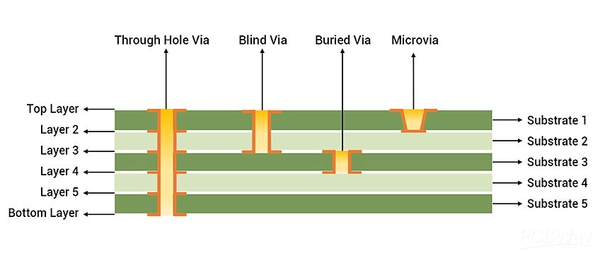
Table: Choosing a via type (practical view)
| Via type | Why you use it | Main downside | What to confirm with the fab |
|---|---|---|---|
| Through via | Lowest risk and common | Uses routing space on all layers | Min drill, annular ring, aspect ratio limits |
| Blind/buried via | More routing channels | Higher cost and process steps | Supported build-up method and yield history |
| Microvia (HDI) | Fine-pitch BGA escape | Tight process window | Laser via capability and allowed structures |
| Via-in-pad | Highest density under BGAs | Why do you use it | Via fill method, planarization, accepted finishes |
Practical tip: only choose HDI when pitch and density force it, and only after the fab confirms they can build it reliably.
Step 5: Placement with “3D awareness”
In multilayer placement, the “space” you manage is not only on the top and bottom. You manage internal routing corridors, plane regions, and where you can safely transition layers. Placement must protect the plane strategy and make the intended layer usage feasible.
After stack-up, return-path rules, and via strategy are defined, you can place parts to match them. If you place earlier, you might create impossible BGA escapes, force too many layer changes, or place noise sources directly above sensitive internal routes.
With multilayer PCBs, what happens on the inner layers matters during placement. You must think in three dimensions.
Use these habits:
- Keep switching regulators and their hot loops tight and away from sensitive analog and RF blocks (protects planes and return paths).
- Place decoupling capacitors close to the IC pins, and make the path to power and ground short (reduces loop inductance into planes).
- Place connectors so fast interfaces can reach a solid reference plane quickly (reduces exposure and EMI).
- Separate noisy and quiet zones. Keep the boundary clear and enforced in routing (prevents plane damage and coupling).
Service-provider test: A good design partner runs a placement review that includes SI/PI and EMC, not only mechanical fit.

Step 6: Routing rules that work in real builds
Routing in multilayer boards is mainly about controlling references and coupling: which layer, which plane, how many vias, and how planes are kept intact. Multilayer routing rules are not just “trace width and clearance.” They include layer-direction planning and plane-aware constraints.
Once placement is stable, routing rules become enforceable. If placement is moving, you will keep breaking the rules and making exceptions, which leads to an inconsistent board that is hard to debug and hard to build.
Do not start routing until you have rules. Set the rules, lock the stack-up, then route.
Practical routing rules:
- Route fast signals adjacent to a solid plane (usually GND) to control impedance and EMI.
- Keep differential pair spacing consistent and avoid unnecessary layer swaps.
- Reduce via count on very fast nets to reduce discontinuities and return-path breaks.
- Route adjacent internal signal layers in perpendicular directions when possible to reduce coupling.
- Keep ground planes intact. Do not cut them unless you have a clear reason and a plan.
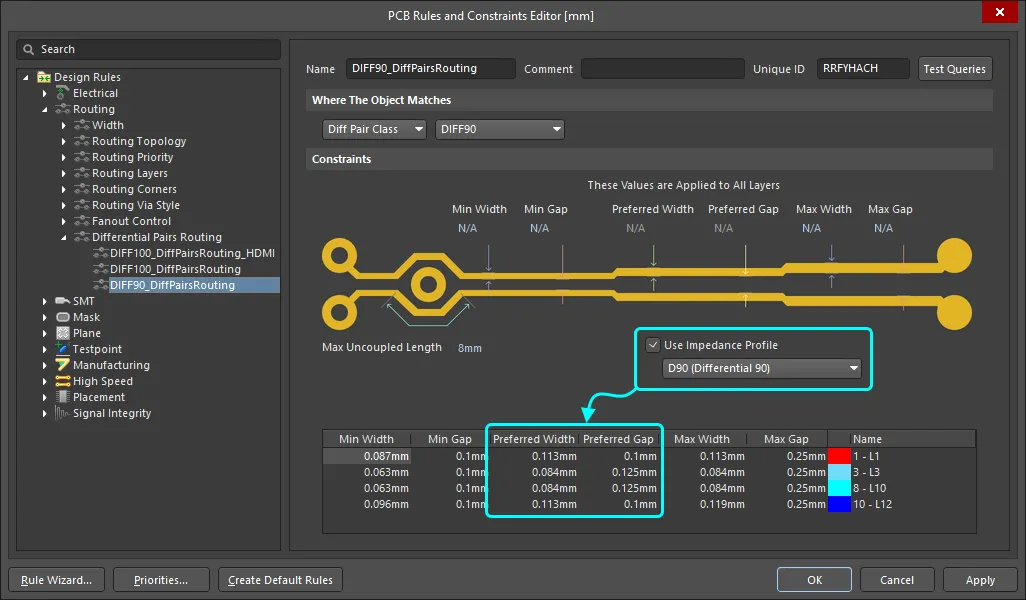
Table: Routing choices by net type
| Net type | Best routing style | Key rule |
|---|---|---|
| Very fast digital | Stripline or microstrip with solid reference | Keep return path continuous and avoid plane splits. |
| Differential pairs | Adjacent to a solid plane | Keep spacing stable and limit layer changes. |
| Sensitive analog | Quiet area with solid ground | Do not share noisy return paths. |
| High current DC | Wide copper and short paths | Size conductors for current and heat, not only impedance. |
Step 7: Power distribution and decoupling
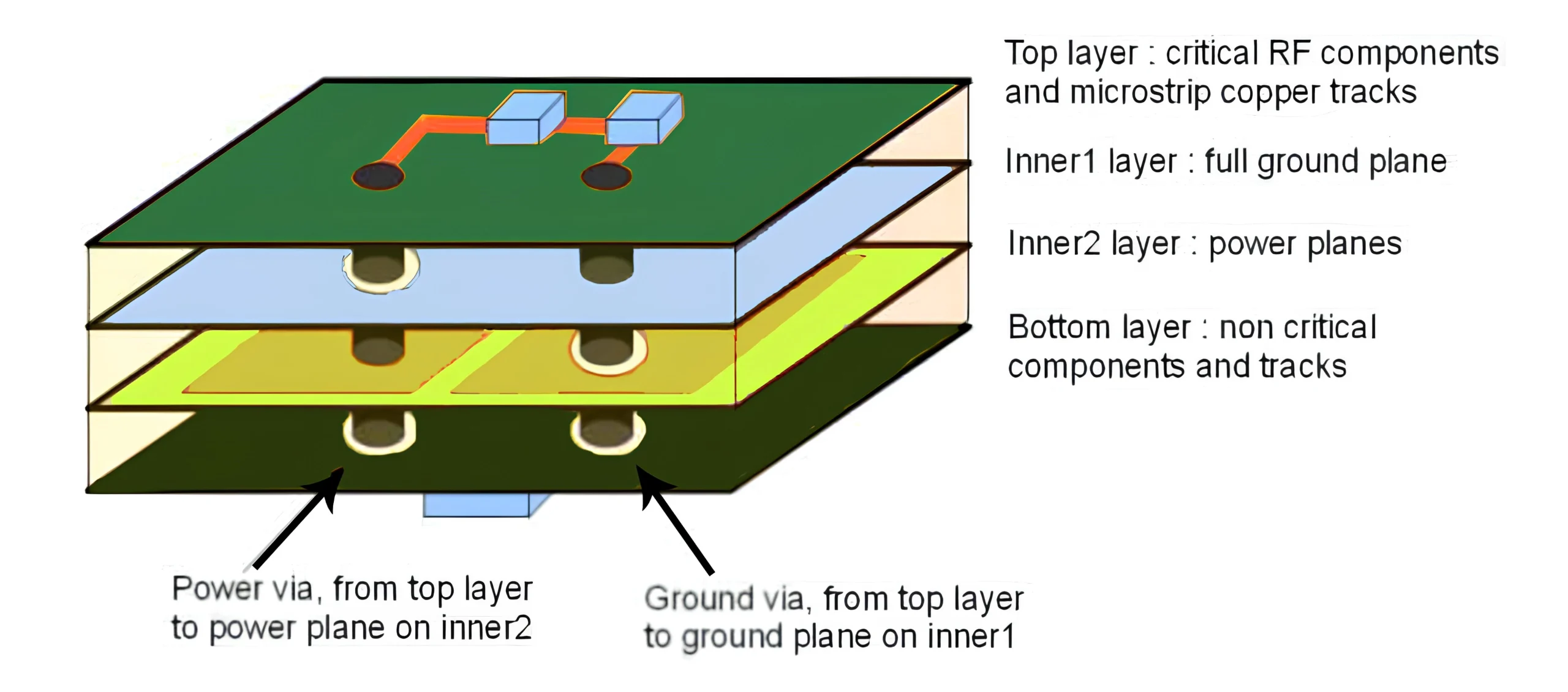
Multilayer boards let you use plane pairs (power + ground) to lower PDN impedance. But the benefit only happens when decoupling connections into the planes are short and when plane integrity is protected. This is a multilayer plane advantage, but it is easy to waste.
After routing rules are in place and critical routing is underway or complete, you can shape power and ground copper with less risk of blocking important routes. Also, you can now see where vias and copper have damaged planes and fix it.
Power design is part of signal quality. It is also part of EMI control.
Good practices:
- Prefer solid planes for main rails when you can (lower impedance).
- If you split planes, keep fast signals away from split edges and do not cross gaps (protect return paths).
- Use multiple decoupling capacitors with short paths, not only one big cap (covers frequency range).
- Use stitching vias to connect ground regions and support return paths (reduces loop area).
Step 8: Thermal management that fits multilayer boards
Internal copper planes can spread heat across the board. Thermal vias can move heat into those planes. This is a major multilayer advantage, but it requires planning that respects assembly constraints and plane strategy.
Thermal features depend on near-final copper, pours, and via placement. If you do thermal too early, routing changes can remove copper you were counting on. If you do it too late, you will not have space left for via arrays and copper spreads.
Higher density means more heat per area. Plan thermal paths early.
Practical techniques:
- Identify hot parts early and reserve copper area around them.
- Use thermal vias under power parts when allowed by assembly and reliability needs.
- Connect thermal vias to internal copper planes that can spread heat.
- Avoid trapping heat under dense shields without a thermal plan.
Service-provider test: ask what thermal checks they run and what standard patterns they use for common power devices.

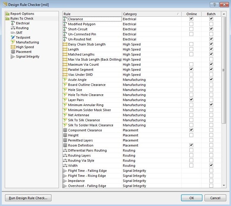
Step 9: DFM and DFA checks (before you export files)
Multilayer DFM is strongly tied to stack-up symmetry, via structures, plane “damage” from drilling/vias, and impedance tolerances. DFA is also impacted by via-in-pad, fine pitch, and how flat pads remain after processing. These are common multilayer failure points.
DFM must match the final geometry. If you check too early, later routing changes can break clearances, create plane voids, or introduce risky via structures. Doing this right before outputs reduces the chance of sending a “buildable yesterday, risky today” design.
DFM is not a final step. It starts with the stack-up and keeps going through routing and documentation.
Pre-layout checklist (copy and use):
- Confirm standard stack-up options with the fab for your layer count and thickness.
- Confirm minimum trace/space and minimum drill.
- Confirm supported via types: blind, buried, microvia, via-in-pad.
- Define layer roles: signal, ground, power.
- Define impedance targets and list the nets that need control.
- Define keepouts and isolation zones for noisy and sensitive areas.
DFM checklist (copy and use):
- Symmetric stack-up and balanced copper distribution to reduce warpage risk.
- Clear reference planes under fast signals.
- No fast signals crossing split planes.
- Via-in-pad rules are defined if used (filled and plated as required).
- Manufacturable geometries: trace/space, hole sizes, mask rules, and clearances match fab capability.
- Clear notes: material, copper weights, finish, impedance targets, tolerances, and any special build requirements.
Practical tip: the smallest possible geometry often lowers yield. Many boards get cheaper when you relax the trace/space and drill sizes a little.
Step 10: Outputs and documentation (what you send to the fab)
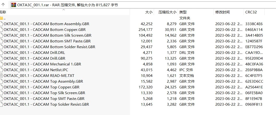
Multilayer builds require explicit documentation of the stack-up, impedance, and via structures. Without that, the fabricator may assume different dielectric thickness, different materials, or different via processing, which can change impedance and reliability. Multilayer documentation is the “contract” that protects your intent.
Outputs must reflect the final checked layout. If you generate outputs earlier, then change routing, you risk version mismatch and build errors. Multilayer projects are especially sensitive because many files and notes must match exactly.
A good output package prevents misunderstandings.
Include:
- Fabrication files for copper, solder mask, and silkscreen, plus drill files.
- A stack-up table with layer order, copper weight, dielectric thickness, and total thickness target.
- An impedance table with target values and tolerances.
- Assembly notes, especially for via-in-pad, fine pitch, and special finishes.
- Test notes if you need specific coverage.
If your manufacturer supports richer formats than Gerbers, it can reduce back-and-forth. Still, the best results come from clear stack-up and clear notes.
Common pitfalls (and how to avoid them)
- You start routing before the stack-up is approved. Fix: lock stack-up and impedance targets first.
- You use an asymmetric stack-up. Fix: keep layer types and dielectrics mirrored and balanced.
- You route fast signals over split planes. Fix: keep reference planes solid under those nets.
- You change layers with no return-path plan. Fix: add stitching vias and keep plane transitions clean.
- You chose HDI without a real need. Fix: Use HDI only when pitch and density force it.
- You use via-in-pad without proper fill and plating. Fix: specify the correct VIP process from the start.
- You over-cut ground planes. Fix: Keep the ground continuously and only split with clear rules.
- You treat thermal as an afterthought. Fix: Reserve copper and thermal via space early.
How do Advanced PCB Tools Support Multilayer and HDI Designs?
Advanced PCB tools help when they keep the design consistent and rule-driven.
They support multilayer PCB design by enabling:
- Stack-up managers that connect layer spacing to impedance planning
- Rule systems for differential pairs, spacing, and length matching
- Via definitions for blind, buried, and microvias, plus checks for illegal transitions
- Strong DRC that catches manufacturability and reliability risks early
- Better documentation outputs so the fab and assembler can follow your intent
If a design service uses advanced tools well, you see fewer manual exceptions, fewer last-minute rule changes, and a cleaner manufacturing package.
Tool notes: Altium, Eagle, OrCAD (workflow view)
How to design a multilayer PCB in Altium?
Set up the layer stack first. Then set impedance and routing rules. Then place and route while running DRC often. At the end, export a complete package with stack-up and impedance documentation.
How to design a multilayer PCB in Eagle?
Keep the layer plan simple and clear. Define net classes for critical signals. Set strict design rules early and keep checking them during routing. Spend extra time on documentation so the fab does not need to guess.
How to design multilayer PCB in OrCAD?
Use constraint-driven design. Attach spacing, impedance, and length rules to the right nets. Keep DRC on and fix issues as you go. Generate outputs with clear stack-up and fabrication notes.
Working with manufacturers (and picking a design service)
Do not pick a provider based on layer count claims. Pick them based on how they reduce risk and how they work with your manufacturer.
What to confirm before layout starts?
Ask these questions:
- What standard stack-ups do you recommend for 4/6/8 layers at my thickness?
- What are your minimum trace/space and minimum finished drill in production?
- Which via types do you support: blind, buried, microvia, via-in-pad?
- Do you support controlled impedance? What tolerance can you hold?
- What materials do you suggest for my speed and loss needs?
- What surface finishes do you recommend for my pitch and reliability goals?
- What testing do you provide, and what is the usual yield for similar builds?
What drives cost in multilayer PCB manufacturing?
Expect these cost drivers:
- Layer count and thickness
- Blind/buried vias and HDI microvias
- Via-in-pad filling and plating
- Controlled impedance and tight tolerances
- Special materials and heavier copper
- Tighter spacing and smaller drills, because yield drops
What a good service provider should deliver?
A strong multilayer PCB design services partner should provide:
- A stack-up proposal with at least two options, plus pros and cons
- A via strategy that matches your fab’s real capability
- Clear constraints: impedance targets, spacing, diff pair rules, length rules
- Placement and routing notes tied to return paths and EMI
- A clean manufacturing package with stack-up, impedance table, and build notes
If you want a quick design review, share your schematic, board outline, main interfaces, and any impedance targets. A good team can suggest a stack-up and via plan before layout starts, and that often saves weeks later.
Before you choose a multilayer PCB design service, these are the questions that usually decide cost, risk, and schedule.
Conclusion
Multilayer PCB design works best when you decide the stack-up, return paths, and via strategy before you start routing. This approach improves SI and EMI, and it also lowers manufacturing risk. If you want to choose the right multilayer PCB design service provider, look for a team that starts with constraints, confirms fab capability early, and delivers a complete manufacturing package with clear documentation. If you’re planning your next multilayer design and need technical support or manufacturing expertise, IWDF Solutions is here to help — from concept to delivery.

