

A piece of industrial equipment runs perfectly today. The board inside it is fine. But the IC it depends on was quietly discontinued two years ago — and you may not know that yet.
PCB reverse engineering for obsolete component replacement recovers a board’s full design documentation from a physical sample — schematic, layout, BOM, and Gerber files — then updates the design to replace discontinued parts with currently available alternatives. The result is a production-ready PCB that no longer depends on components your supply chain cannot deliver.
The reason most manufacturers get caught off guard is simple: a discontinued component does not stop your production immediately. Your existing stock carries you through months, sometimes years. The urgency is invisible — until the buffer runs out. By that point, the last-time-buy window has closed, authorized distributors no longer carry stock, and the only remaining supply comes from gray-market sources, where counterfeit risk is high and traceability is zero. If your original design files were with an engineer who left a long time ago, or with a PCB supplier who shut down, you are now facing a production halt with no recovery path. The manufacturers who avoid this outcome do not react to EOL notices — they act before the notice arrives. PCB reverse engineering restores design ownership and eliminates the dependency before the supply line breaks.
This article is written for engineers, procurement managers, and operations teams who either face an EOL problem right now or want to prevent one. It covers what PCB reverse engineering for obsolete component replacement actually involves at the technical level, where most projects go wrong, what industry-specific factors shape the process, and how to evaluate a service provider before you commit.

Is PCB Reverse Engineering the Right Response to an EOL Problem?
When a production component reaches End-of-Life, there are four common responses. Three of them fail in specific ways. PCB reverse engineering addresses the root problem the others cannot — because it restores design ownership, not just temporary access to parts.
| Response | When It Appears to Work | Why It Often Fails |
|---|---|---|
| Last-time buy (LTB) | Part is still available in limited supply | Finite. Does not solve future production. Ties up capital. |
| Drop-in part substitution | A pin/package/function-compatible part exists | Rarely true for specialized ICs without full engineering validation |
| Secondary market sourcing | Emergency quantities can be found | High counterfeit risk, no quality assurance, no long-term supply |
| PCB reverse engineering + redesign | Original files are unavailable; no validated drop-in exists | Requires engineering investment and a capable provider |
Why “Find a Replacement Part” Is Harder Than It Looks?
The first instinct is to search for a functionally equivalent replacement. Sometimes that works. More often, it does not — for reasons that are not visible from a part number lookup.
Pinout differences. Two ICs can do the same job but have their pins in different positions. Substituting one for the other without updating the PCB layout will cause the board to fail — and may damage it.
Package incompatibility. The original part may be a DIP-16. The modern equivalent is a QFN-16. Same pin count, completely different land pattern, pad geometry, and solder process. The board must be physically redesigned.
Register and protocol differences. For microcontrollers and power management ICs, firmware may need to be updated to match new register maps or initialization sequences. This is not a layout change — it is a firmware change — and it must be evaluated before the replacement is selected.
Thermal profile mismatch. A newer IC may run at different temperatures or require a thermal pad the original did not have. Using it on a board designed for its predecessor causes reliability failures in the field — failures that may not appear during initial testing.
None of these problems are visible from a distributor’s catalog. They require a full engineering review of the original board and both datasheets. That review is the core value that professional PCB reverse engineering delivers.

What Does PCB Reverse Engineering Actually Involve?
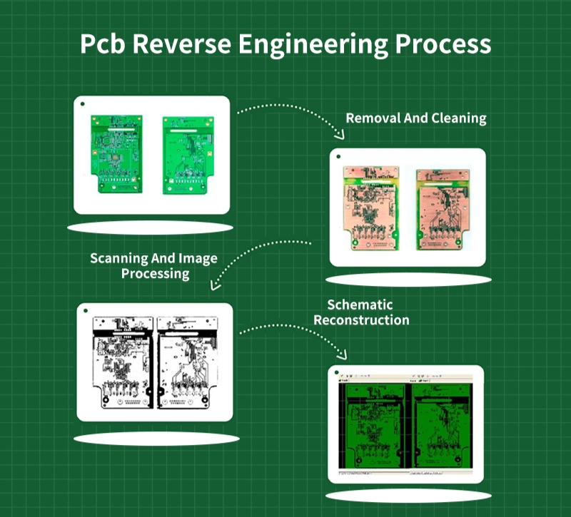
Most descriptions of this process stop at “we scan the board and recover the Gerbers.” That is a fraction of what competent reverse engineering involves — and it is not sufficient when the goal is to replace obsolete components, not just copy the original.
PCB reverse engineering for obsolete component replacement is a multi-phase engineering process. The physical analysis phase is the starting point. The engineering work that follows — schematic reconstruction, BOM recovery, EOL evaluation, and layout redesign — is where the real work happens and where the deliverable gains its value.
Phase 1 — Physical Analysis and Layer Mapping
The process starts with the board itself. Engineers photograph both sides at high resolution, record every component, and document part numbers, package types, reference designators, and orientations.
For multi-layer boards — which represent most industrial, medical, and automotive electronics — visual inspection alone is not enough. Internal layers cannot be seen from the outside. X-ray scanning maps via locations, internal routing paths, and layer stack-up. For HDI boards with blind vias, buried vias, or microvias, X-ray analysis is not optional. It is the only way to confirm internal connectivity without destructive testing.
Missing a buried via at this stage creates routing errors that do not appear until the board has already been fabricated. Catching them before fabrication is the point.
A second challenge is unique to boards from OEM manufacturers: the component markings have been deliberately sanded off or covered to prevent copying. When standard part identification fails, engineers use circuit context — supply voltage, pin connectivity, surrounding passive values, and functional block analysis — to determine the component’s identity. This takes longer than reading a label. It is the only available method when labels are absent.
Phase 2 — Schematic Reconstruction
With physical data collected, engineers trace every net and reconstruct the complete schematic in professional EDA software.
| EDA Tool | Common Application | Output Format |
|---|---|---|
| Altium Designer | Industrial, automotive, high-speed digital | .SchDoc / .PcbDoc |
| KiCad | Open-source, cost-sensitive projects | .kicad_sch / .kicad_pcb |
| OrCAD | Legacy telecom and industrial | .DSN / .BRD |
| Cadence Allegro | High-density, server, RF designs | .SCH / .BRD |
This phase requires engineering judgment, not just net tracing. A schematic represents functional intent, not just connection topology. A reverse engineer must understand what each circuit block does — power management, differential signaling, MCU peripheral interfaces, analog signal conditioning — to reconstruct it accurately and to make credible substitution decisions later.
Phase 3 — BOM Recovery and EOL Component Evaluation
The Bill of Materials is reconstructed from the physical board and the schematic. Each component is confirmed against its datasheet. Current market availability is checked. EOL components are flagged.
For every flagged EOL component, the engineering evaluation covers:
- Electrical equivalence: voltage ratings, current ratings, logic levels, timing, frequency response, communication protocol
- Package compatibility: same footprint, same pitch, same land pattern — or documented differences requiring layout changes
- Pinout mapping: pin-by-pin comparison against both datasheets
- Thermal requirements: power dissipation, thermal pad specifications, operating temperature range
- Regulatory compliance: RoHS, REACH, and any applicable industry standard (ISO13485, IATF16949)
This evaluation produces a substitution recommendation with a documented rationale. It is the paper trail a procurement team or quality manager needs to justify the change internally.
Phase 4 — PCB Layout Reconstruction and Redesign
The PCB layout is rebuilt in CAD, incorporating all changes required by the EOL substitutions. New footprints replace obsolete component pads. Traces are rerouted where pinout differences changed net assignments. Power planes or decoupling networks are updated where the replacement IC has different supply requirements.
The output is not a copy of the original board. It is an engineered revision — functionally equivalent to the original, free from EOL dependencies, and ready for production.
Phase 5 — Deliverable Package
| Deliverable | Why It Matters |
|---|---|
| Editable schematic file | Allows future modifications; Gerbers alone cannot be edited |
| Editable PCB layout file | Same reason — source files, not just output files |
| Gerber files (all layers) | Manufacturing-ready output for fabrication |
| Updated BOM with replacement components | Includes sourcing options and qualification notes |
| Pick-and-Place / Centroid file | Required for SMT assembly line programming |
| 3D board rendering (optional) | Used for mechanical clearance verification |
If a provider delivers Gerbers only — without editable source files — you do not own the design. Any future change, no matter how small, requires restarting the entire reverse engineering process. Always confirm this point in writing before signing a contract.
Where Do EOL Redesign Projects Actually Fail?
EOL-driven reverse engineering is more complex than standard board copying — and it fails in predictable ways. Understanding the failure modes before the project starts is the best way to avoid them.
Most providers can scan a board and recover a BOM. Fewer can execute the engineering steps that follow. The three most common failure points are below.
Failure Point 1 — Footprint Mismatch After Package Change
When a replacement IC uses a different package than the original, the PCB footprint must be updated. A footprint is the physical pad pattern on the board where the component is soldered. Pad size, pad spacing (pitch), copper land area, and solder mask opening all affect whether the component solders correctly.
A footprint mismatch causes assembly problems. If paste stencil apertures are sized for the old component and the new component’s pads are smaller, tombstoning and solder bridging become likely during reflow. If pad pitch does not match the IC’s pin pitch, the board cannot be assembled at all.
Footprint errors are among the most common causes of first-article assembly failures. Catching them at the redesign stage — before fabrication — prevents costly prototype respins.
Failure Point 2 — Pinout Difference Without Rerouting
Two ICs that perform the same function may have completely different pin assignments. This is common when transitioning from an older generation to a newer one within the same product family. Same function, different pinout.
When a provider simply swaps the component designator without reviewing the datasheets, the board appears correct on paper. When power is applied, nets are connected to wrong pins. At best, the board is non-functional. At worst, supply rails short through I/O pins.
The correct process is a full pin-by-pin comparison of both datasheets, followed by trace rerouting for every pin that changed assignment. The change is documented in the revised schematic so it is fully traceable.
Failure Point 3 — Ignoring Thermal and Mechanical Constraints
A replacement component may dissipate more heat than the original. It may be physically taller, affecting clearance to a cover or heatsink. It may require a thermal pad on the PCB that the original did not.
These are not paper issues. They cause field failures — boards that pass electrical testing but overheat in the application environment, or assemblies that do not fit their enclosures after modification.
Thermal analysis is required for any replacement component whose power dissipation differs from the original. Mechanical clearance should be verified in the 3D model before fabrication. These checks are not expensive. Skipping them is.

Which Industries Are Most Affected by EOL Component Obsolescence?
Component obsolescence does not affect all industries equally. The sectors most exposed are those with the longest product lifecycles — where the gap between component availability and product service life is widest and where replacing the product is not a practical option.
The numbers show how serious this has become. Nearly 750,000 electronic parts went obsolete in 2022. The rate moderated slightly in 2023, but EOL notices still exceeded 470,000 that year. Products designed for 10–20-year operational lifecycles face a growing mismatch between how long equipment is expected to run and how long its components remain in production.
Understanding how redesign projects fail is only half the picture. The other half is knowing who gets hit hardest — because the industry a board serves shapes how urgent the redesign decision actually is.
Industrial Automation and Control Systems
Industrial PLCs, motor drives, CNC controllers, and HMI panels are designed to run for 20 years or more. The ICs inside them were designed for consumer electronics timelines — 5 to 7 years before EOL.
When a critical IC in a PLC module is discontinued, the practical options are narrow: replace the entire machine (capital cost, installation, retraining), wait for an OEM support contract that may not cover component-level repairs, or reverse engineer the board and redesign around an available replacement. The third option is the only one that preserves the equipment investment without production disruption.
Medical Devices
Medical devices carry multi-decade operational obligations under their regulatory approvals. When a component in a certified device goes EOL, the replacement must be validated and documented to satisfy the requirements of the applicable regulatory framework.
This is where engineering intersects with quality management. Identifying and qualifying a replacement component in a medical device is a documented change control activity. It feeds into the device’s technical file and may require re-submission to a notified body, depending on the scope of the change. A reverse engineering provider working in the medical sector must understand this — and must produce documentation that supports the change control process.
ISO13485 is the international quality management standard for medical device manufacturing. A provider without this certification is not operating under the documented quality discipline that medical device manufacturers require from their supply chain partners.
Automotive Electronics
Vehicles have service lives of 10 to 20 years. OEMs and aftermarket suppliers must support board-level repairs throughout that window. When a primary IC in an ECU is discontinued, the manufacturer faces a direct choice: halt production of replacement assemblies, or reverse engineer and redesign.
For high-volume applications — body control modules, instrument clusters, ADAS sensor processors — redesigning around an EOL part extends the serviceable life of the vehicle platform. IATF16949 is the quality management standard for automotive electronics manufacturing. For automotive customers, it is a procurement requirement.
Aerospace and Defense
Aerospace and defense programs operate on acquisition and service timelines that routinely exceed 30 years. Electronics commissioned on a platform in 2000 may still be in active service in 2030 or beyond. Component obsolescence is a formally recognized program risk in major defense acquisition frameworks.
Boards in this sector are often complex — high layer counts, controlled impedance, ceramic substrates, radiation-hardened components. X-ray analysis, precise multi-layer reconstruction, and validated BOM substitution are all standard requirements. The margin for error in the field is effectively zero.

What Should You Ask a PCB Reverse Engineering Provider Before You Commit?
Choosing the wrong provider for an EOL redesign project means receiving files that cannot be used — Gerbers without source files, BOMs with unvalidated substitutions, or layouts with footprint errors that surface at first article. Asking the right questions before you engage is the most direct way to distinguish a capable provider from one that delivers partial work.
Provider Evaluation Checklist
| Question | What the Right Answer Looks Like |
|---|---|
| What deliverables do I receive? | Editable source files (schematic + layout) plus Gerbers. Gerbers alone are not sufficient. |
| Can you handle multi-layer HDI boards? | Yes — with in-house X-ray scanning equipment. Ask specifically about blind and buried vias. |
| Do you update footprints and reroute traces for EOL replacements? | Yes — with a specific description of the footprint update and pin-mapping review process. |
| What certifications does your factory hold? | ISO9001 minimum. ISO13485 for medical. IATF16949 for automotive. |
| Do you sign NDA agreements? | Yes, before any board or design information is shared. |
| Do you manufacture in-house? | Yes — same team does design and fabrication, eliminating DFM errors at handoff. |
Why Manufacturing Integration Matters for This Type of Project?
A design file that passes DRC in the EDA tool may still have features a specific factory cannot manufacture — minimum via diameters that exceed the factory’s drill capability, copper-to-edge clearances requiring special tooling, or impedance targets the available laminates cannot achieve.
When the reverse engineering team and the manufacturing team are the same entity, DFM constraints are incorporated during the reconstruction phase — not discovered during a factory review that delays the timeline by two weeks after files are submitted.
This matters more for EOL projects than for standard new designs. EOL projects are already running behind schedule. Every additional iteration extends the production disruption that started when the EOL notice arrived.
Why Does the One-Stop Service Model Change the Outcome?
PCB reverse engineering for obsolete component replacement spans multiple technical disciplines: physical analysis, schematic capture, EDA layout, component sourcing, DFM review, fabrication, and SMT assembly. Managing these across separate vendors introduces delays and errors at every handoff.
A one-stop provider handles the full workflow under one roof. This is not a convenience argument — it is a lead time and quality argument.
| Service Stage | Multiple Vendors | One-Stop Provider |
|---|---|---|
| Physical board analysis and imaging | Vendor 1 | In-house |
| Schematic and layout reconstruction | Vendor 2 | Same team |
| EOL component evaluation and BOM update | Vendor 2 or separate consultant | Same team |
| Component sourcing | Vendor 3 | In-house procurement |
| PCB fabrication | Vendor 4 | Same factory |
| SMT assembly | Vendor 4 or 5 | Same facility |
| Functional testing | Vendor 5 or 6 | Same facility |
Each vendor handoff adds coordination time, file format translation risk, and the possibility that undocumented design assumptions cause errors requiring iteration. For EOL projects — where production continuity is already interrupted — additional delays compound the business cost.
IWDF Solutions covers the full workflow in-house. The table below shows the specific technical parameters supported across the facility.
| Capability | Specification |
|---|---|
| Layer count | 2 to 20 layers |
| Via types | Through-hole, blind, buried, microvia (HDI) |
| Component support | BGA, QFN, SOP, DIP, fine-pitch ICs, passive arrays |
| Board types | Rigid, flexible (FPC), rigid-flex |
| EDA tools | Altium Designer, KiCad, OrCAD, Cadence Allegro |
| Turnaround — 2-layer | 5–10 working days |
| Turnaround — multi-layer / HDI | 10–20 working days |
| Certifications | ISO9001:2015, IATF16949, ISO13485, RoHS, REACH |
Shenzhen’s supply chain concentration — the density of component distributors, specialty materials suppliers, and PCB process expertise in the Pearl River Delta — means that component sourcing for replacement parts happens in parallel with design reconstruction, not sequentially after it. This routinely cuts two to four weeks from a project timeline compared to coordinating the same work across geographies.
Frequently Asked Questions
What is PCB reverse engineering for obsolete component replacement?
It is the process of analyzing a physical circuit board — without original design files — to recover its full design documentation, then engineering an updated version that replaces EOL components with currently available parts. The deliverable is a production-ready PCB design with no dependency on discontinued components. It is distinct from simple board copying, which produces a replica of the original without addressing the supply chain problem.
What is the difference between PCB reverse engineering, PCB cloning, and PCB copying?
PCB copying or cloning means producing an identical replica of an existing board. PCB reverse engineering means recovering full editable design documentation — schematic, layout, BOM, Gerber files — that enables future modifications and independent production. EOL-driven reverse engineering combines documentation recovery with active design modification to eliminate discontinued component dependencies. Cloning gives you a copy. Reverse engineering gives you ownership of the design.
Can a board be reverse engineered if the component markings have been sanded off?
Yes. When part markings are missing or deliberately removed, component identification uses circuit context: supply voltage, pin connectivity, surrounding passive values, and functional block analysis. For microcontrollers and other programmable devices with protected firmware, IC decryption services can recover the embedded code, enabling migration to a modern equivalent. This is standard practice for boards where the original supplier intentionally obscured identification.
What happens when no direct pin-compatible replacement exists for an EOL component?
This is common for proprietary ASICs and discontinued microcontrollers. Three engineering paths are available: use an interposer PCB to bridge the footprint difference; select a replacement with a different pinout and reroute the affected traces; or recover the original firmware through IC decryption and migrate to a modern MCU. The right choice depends on the complexity of the change and the functional constraints of the board. The decision should be made after evaluating all three options — not defaulting to one without reviewing the others.
How is electrical equivalence confirmed for a replacement component?
Equivalence requires a side-by-side datasheet review covering operating voltage range, logic levels, output drive current, frequency response, communication protocol and register map, timing parameters, and power consumption. Physical equivalence requires confirming package dimensions, pad pitch, thermal pad geometry, and component height. A replacement that passes this review is a validated substitute. A replacement selected from a distributor catalog without this review is a risk — even if the functional description appears identical.
What certifications should a PCB reverse engineering provider hold?
ISO9001:2015 is the baseline for general quality management. ISO13485 is required for medical device manufacturing. IATF16949 is required for automotive applications. RoHS and REACH compliance is a baseline requirement for components and finished boards shipped to the EU and most other regulated markets. In regulated industries, these certifications are not optional — they are procurement requirements enforced through supplier qualification audits.
How long does a reverse engineering and EOL redesign project typically take?
For a 2-layer board with standard SMT and through-hole components, the reverse engineering and redesign phase is approximately 5–10 working days. For complex multi-layer boards (8+ layers), HDI structures, or boards with multiple EOL components requiring significant layout changes, the timeline is 10–20 working days. Prototype fabrication and assembly add time on top of this, depending on board complexity and order quantity.
Do I need to ship the physical board to begin?
Not to get started. High-resolution photographs of both sides of the board, with dimensions and any partial documentation available, are enough for an initial engineering assessment and project quotation. The physical board is required before engineering work begins. NDA signing can happen before any board or design information is shared.
Is PCB reverse engineering legal?
In most jurisdictions, reverse engineering a product you own for the purpose of repair, maintenance, internal production continuity, or interoperability is legal and commercially recognized. The legal analysis becomes more complex when the objective is to compete directly with the original manufacturer or to reproduce a patented design for sale to third parties. For the use cases covered in this article — EOL replacement, long-term service support, and production continuity — reverse engineering is standard engineering practice. IWDF Solutions works within these legal boundaries and conducts an initial project review to confirm scope before any engineering work begins.
Why choose a Shenzhen-based provider over a local reverse engineering service?
Shenzhen’s supply chain concentration makes component sourcing for replacement parts faster and more reliable. An in-house factory in Shenzhen has direct access to the component distributors, specialty laminates, SMT equipment, and process chemistry that determine whether a redesign can be manufactured efficiently and at the right cost. Beyond sourcing, the cost of engineering hours and prototype production in Shenzhen is substantially lower than equivalent work in Europe or North America — without sacrificing quality when the provider holds the appropriate certifications and operates documented quality management processes.
IWDF Solutions is a Shenzhen-based PCB manufacturer and engineering services provider specializing in PCB reverse engineering, PCB design, PCB manufacturing, and PCBA production. With over 20 years of experience and certifications covering ISO9001:2015, IATF16949, and ISO13485, IWDF Solutions supports clients in industrial, medical, automotive, aerospace, and consumer electronics sectors from initial board assessment through volume production.

