

A PCB failure in a fighter jet doesn’t generate a warranty claim. It generates a crash report. Most suppliers claim aerospace capability. Very few can prove it.
Aerospace PCB assembly requires IPC-A-610 Class 3, AS9100D certification, MIL-PRF-31032 compliance, and full component traceability from raw material to finished board. This article covers the specific standards, design constraints, production environment requirements, and supplier criteria that determine whether your aerospace or defense PCB program succeeds or fails in production.
The global aerospace and defense PCB market was valued at approximately $3.87 billion in 2025 and is projected to reach $6.16 billion by 2034, driven by UAV platforms, next-generation avionics, satellite programs, and C4ISR system upgrades. Behind every one of those programs is a PCB — and a manufacturer who was either qualified for the job or wasn’t. This article breaks down what “qualified” actually means, from the certifications on the wall to the ESD-controlled floor under the assembly line.

What Makes Aerospace PCB Assembly Fundamentally Different From Standard Production?
Most PCB suppliers describe their work as “high-reliability.” In aerospace, that phrase has a specific technical definition — and most commercial manufacturers don’t come close to meeting it.
Aerospace PCBs must survive -55°C to +125°C temperature swings, constant mechanical vibration, pressure differentials at altitude, and in space applications, cumulative radiation exposure. Standard commercial production manages defect rates in parts per million. Aerospace programs require defect rates that are effectively zero — because the one that failed might be inside a flight control module.
Three structural differences define this separation from commercial PCB manufacturing.
The Operating Environment Is Hostile by Default
A radar processing board on a military aircraft can experience:
- Temperature swings from -55°C at altitude to +125°C near engine exhaust, within the same flight
- Continuous vibration at frequencies between 10 Hz and 2,000 Hz during operation
- Altitude-induced pressure differentials that stress via plating and component adhesion
- Salt spray and chemical exposure on naval platforms
- Total ionizing radiation doses in low-earth orbit that degrade semiconductor junctions over the mission life
Standard FR4 with Class 2 assembly doesn’t survive those conditions reliably. Properly specified aerospace PCBs are built with qualified substrate materials and Class 3 or Class 3A assembly processes engineered for those exact loads.
These Platforms Stay in Service for Decades
Defense platforms operate for 20 to 40 years. The F-16 first flew in 1974. Variants are still in active service today. PCBs inside those systems must be designed for that lifespan from day one. When components go obsolete, replacement boards must be re-fabricated to exact specification. This is why PCB reverse engineering is a relevant capability for aerospace programs — not a niche service. Legacy hardware without surviving documentation is a real program management problem, and recovering that documentation from a physical board is often the only path forward.
There Is No Acceptable Field Failure Rate
In commercial electronics, a 0.1% field failure rate is a support cost. In aerospace and defense, it is a safety investigation and a potential loss of life. Every process decision — material selection, reflow profile, inspection method, test coverage — is made with one constraint: the board must not fail in service.

Which Certifications Actually Qualify a Manufacturer for Aerospace Work?
The core certifications for aerospace PCB assembly are AS9100D, IPC-A-610 Class 3 or 3A, IPC-6012DS, MIL-PRF-31032, and J-STD-001 with the Space and Military Addendum. Each covers a different layer of the supply chain. All are required to fully qualify a manufacturer for mission-critical programs.
AS9100D — The Foundation of the Entire Quality System
AS9100D is the aerospace-specific quality management system standard. It builds on ISO 9001 and adds requirements that commercial quality systems don’t address:
- Formal risk management — documented procedures to identify and control risks to flight safety at the production process level
- Configuration management — every engineering change is tracked, controlled, and traceable to the specific production lot it affects
- Counterfeit parts prevention per AS5553 — documented supplier vetting and component authentication procedures, not informal practices
- First Article Inspection (FAI) per AS9102B — the first production unit is fully verified against all dimensional and functional requirements before the production run begins
- Supplier flow-down — AS9100 obligations extend to every sub-supplier in the chain, including raw laminate suppliers
ISO 9001 is the baseline for quality management. AS9100D is the actual aerospace requirement. Do not accept one as a substitute for the other.
The Full Certification Stack and What Each One Covers
| Certification / Standard | Scope | Who Requires It |
|---|---|---|
| AS9100D | Full quality management system | All major aerospace OEMs and prime contractors |
| IPC-A-610 Class 3 / 3A | Assembled board acceptability | Aerospace programs; 3A for space and military avionics |
| IPC-6012DS | Rigid PCB fabrication for space and military | Defense and space programs; addendum to IPC-6012D |
| MIL-PRF-31032 | Military PCB performance specification | All DoD programs; DLA-certified manufacturers only |
| J-STD-001 Space/Military Addendum | Soldering materials and methods | Military and space assembly programs |
| Nadcap | Special process accreditation (soldering, NDT) | Prime contractor flow-down for critical programs |
| IPC-CC-830C | Conformal coating materials and application | All aerospace assemblies requiring environmental protection |
| IPC-7711/7721 | Rework and repair of assemblies | Repair and maintenance programs |
What IPC-A-610 Classes Actually Mean in Practice
| Class | Application | Solder Joint Requirement | Typical Defect Tolerance |
|---|---|---|---|
| Class 1 | Consumer electronics | Basic function; some defects permitted | High |
| Class 2 | Industrial, extended-life | Reduced defect tolerance | Moderate |
| Class 3 | Aerospace, defense, medical | No acceptable defects; continuous operation | Effectively zero |
| Class 3A | Space and military avionics | Class 3 + BGA void limits; coplanarity under 50 µm | Zero |
Class 3 reliability is not achieved through inspection alone. It must be built into the process through locked reflow profiles, controlled stencil apertures, nitrogen reflow atmosphere, and IPC-certified inspectors at every stage.
What PCB Materials Are Right for Aerospace Applications?
Aerospace PCBs use Rogers RO4000 series, PTFE laminates, polyimide, and hybrid constructions based on frequency range, temperature environment, and mechanical load. Material selection must be locked at the earliest design stage — it drives the entire stack-up geometry, impedance calculations, thermal design, and fabrication process.
Core Material Options and Their Application Fit
| Material | Dk | Df | Max Temp | Best Application |
|---|---|---|---|---|
| Rogers RO4003C | 3.55 | 0.0027 | 280°C | Avionics RF circuits, 500 MHz–40 GHz |
| Rogers RT/duroid 5880 | 2.20 | 0.0009 | 260°C | Satellite comms, mmWave arrays, DC–110 GHz |
| Rogers RO3003 | 3.00 | 0.0010 | 250°C | EW systems, 24–40 GHz |
| Polyimide / FR408HR | 3.65 | 0.0090 | 280°C | Rigid-flex, high-temperature environments |
| High-Tg FR4 (Tg 170+) | 4.2–4.6 | 0.020–0.024 | 170°C | Secondary power and digital logic circuits |
| PTFE ceramic composite | 2.17–10.2 | 0.0008–0.0020 | 260°C+ | Space-grade radar, phased arrays |
Hybrid stack-ups — combining Rogers high-frequency layers for RF signal layers with FR4 or polyimide core layers for power and digital layers — deliver the RF performance needed for radar and communication circuits while reducing overall material cost. The key engineering concern in hybrid stack-ups is the CTE mismatch between the two materials. That mismatch generates internal stress at layer interfaces during thermal cycling. Material qualification testing is therefore a direct reliability requirement, not paperwork.
What Design Requirements Must Aerospace PCBs Meet Before Manufacturing Begins?
Aerospace PCB design requirements go significantly beyond the spacing rules and layer count decisions that apply to standard commercial designs. The differences are structural — they affect how the board is laid out, how the stack-up is constructed, how the schematic handles failure modes, and how the design package is documented before a single file is sent to fabrication.
How Aerospace PCB Design Differs From Standard PCB Design?
This table shows where aerospace design rules differ from standard commercial design rules, and why each difference exists:
| Design Parameter | Standard Commercial PCB | Aerospace PCB | Why It Matters |
|---|---|---|---|
| Dielectric minimum thickness | 2.8 mil acceptable | 3.5 mil minimum | Mechanical strength under vibration |
| Trace clearance rule | 3W where practical | 3W mandatory between high-speed signals | Crosstalk control under EMI-dense conditions |
| Via barrel plating | 0.8 mil minimum (Class 2) | 1.0 mil minimum (Class 3, IPC-6012DS) | Fatigue resistance across thermal cycles |
| Controlled impedance tolerance | ±15% typical | ±10% mandatory | Signal integrity at 10 Gbps+ speeds |
| Annular ring minimum | 1 mil (standard) | 2 mil minimum (Class 3A) | Prevents pad separation under mechanical load |
| Solder mask over copper | Optional for some layers | Mandatory with defined thickness | Prevents ionic contamination in humid environments |
| Stack-up symmetry | Recommended | Mandatory | Prevents board warpage during solder reflow and thermal cycling |
| Net redundancy | Rarely required | Required for safety-critical signal paths | Single-point failure prevention on flight-critical nets |
| Component substitution | Often permitted with engineering approval | Controlled — requires formal deviation documentation | Maintains traceability of as-built configuration |
| Design review stage | Informal or optional | Formal DFM review + IPC-6012DS compliance check | Catches fabrication-blocking errors before they reach the factory |
Impedance Control and Signal Integrity
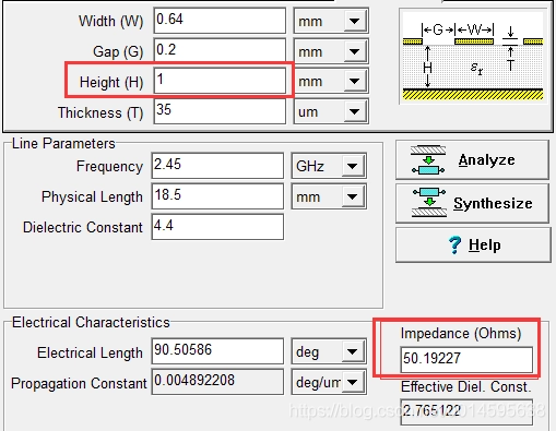
Avionics signal processors operate at speeds up to 10 Gbps. At those speeds, trace geometry directly controls signal quality. Controlled impedance design requires:
- Trace widths and spacing calculated to target impedance — 50Ω single-ended, 100Ω differential pair are standard in aerospace RF and high-speed digital circuits
- Tolerances held to ±10% across the full operating temperature range
- Differential pair length matching within 5 mils on critical high-speed nets
- Via stub minimization — back-drilling or blind vias are used to eliminate resonance caused by unused via sections on high-speed signal paths
- Dielectric constant verified per production laminate lot — not assumed from the nominal datasheet value
A designer who specifies these requirements without confirming that the fabricator can verify them per lot is making a reliability assumption, not a reliability guarantee.
Thermal Management Architecture
Temperature rise above 85°C at critical components accelerates aging exponentially and reduces the useful life of the assembly. Thermal management in aerospace is a structural design decision made at the layout stage — not a thermal pad applied at the end:
- Heavy copper layers (3 oz to 20 oz for high-current power circuits) provide both current-carrying capacity and lateral heat spreading
- Thermal via arrays — dense grids of filled and planarized vias transfer heat from hot component pads through the board to internal thermal planes or chassis mounting points
- Component orientation — high-dissipation devices are placed at board edges or directly above chassis mounting points for conduction cooling paths
- Metal-core substrates (MCPCB) are used for power converter and motor drive boards where heat flux density exceeds what standard laminate thermal vias can manage
EMC and Ground Plane Architecture
Aerospace boards operate in electromagnetic environments that commercial boards are never exposed to — radar transmitters, communication system power amplifiers, and high-current switching converters all on the same platform. EMC design in aerospace is a structural constraint, not a post-layout add-on:
- Analog and digital circuit blocks are physically separated, with ground isolation between sections
- A continuous, uninterrupted reference ground plane is maintained beneath every high-speed signal layer
- RF circuits are compartmentalized using integral shielding walls tied to the ground plane on multiple via stitches per side
- Decoupling capacitors are placed within 0.5 mm of power supply pins on all high-frequency active devices
- Return current paths are explicitly managed — every high-speed trace has a direct return conductor running parallel or directly beneath it
Redundancy and Failure Mode Design
Standard commercial designs rarely implement circuit-level redundancy. Aerospace designs frequently require it. For safety-critical functions — flight control, navigation signal acquisition, power management — the design must include:
- Dual-redundant signal paths for sensors and processors on flight-critical functions
- Watchdog circuits that detect a locked-up processor and force a hardware reset without crew intervention
- Power supply sequencing control to prevent latch-up in complex ASICs and FPGAs during power cycling
- Built-in test (BIT) circuits that allow the system to self-diagnose faults during power-on and during operation
A design that implements these requirements adds board area and component count. A design that skips them saves cost at design time and creates a single-point failure risk that disqualifies the board from flight programs.
Documentation Requirements Before Fabrication
In standard commercial production, sending Gerber files and a BOM is sufficient to start fabrication. In aerospace, the documentation package that precedes fabrication is itself a quality deliverable:
- Controlled impedance table with layer assignment and target values
- Stack-up drawing with specified laminate material, lot-level Dk requirement, and copper weight per layer
- Drill drawing with aspect ratio calculations for all via types
- Assembly drawing with IPC-A-610 Class designation and customer-specific workmanship requirements noted
- BOM with approved manufacturer part numbers (AMPNs) and approved alternates only — no open-market equivalents

How Is Aerospace PCB Assembly Actually Executed at the Production Stage?
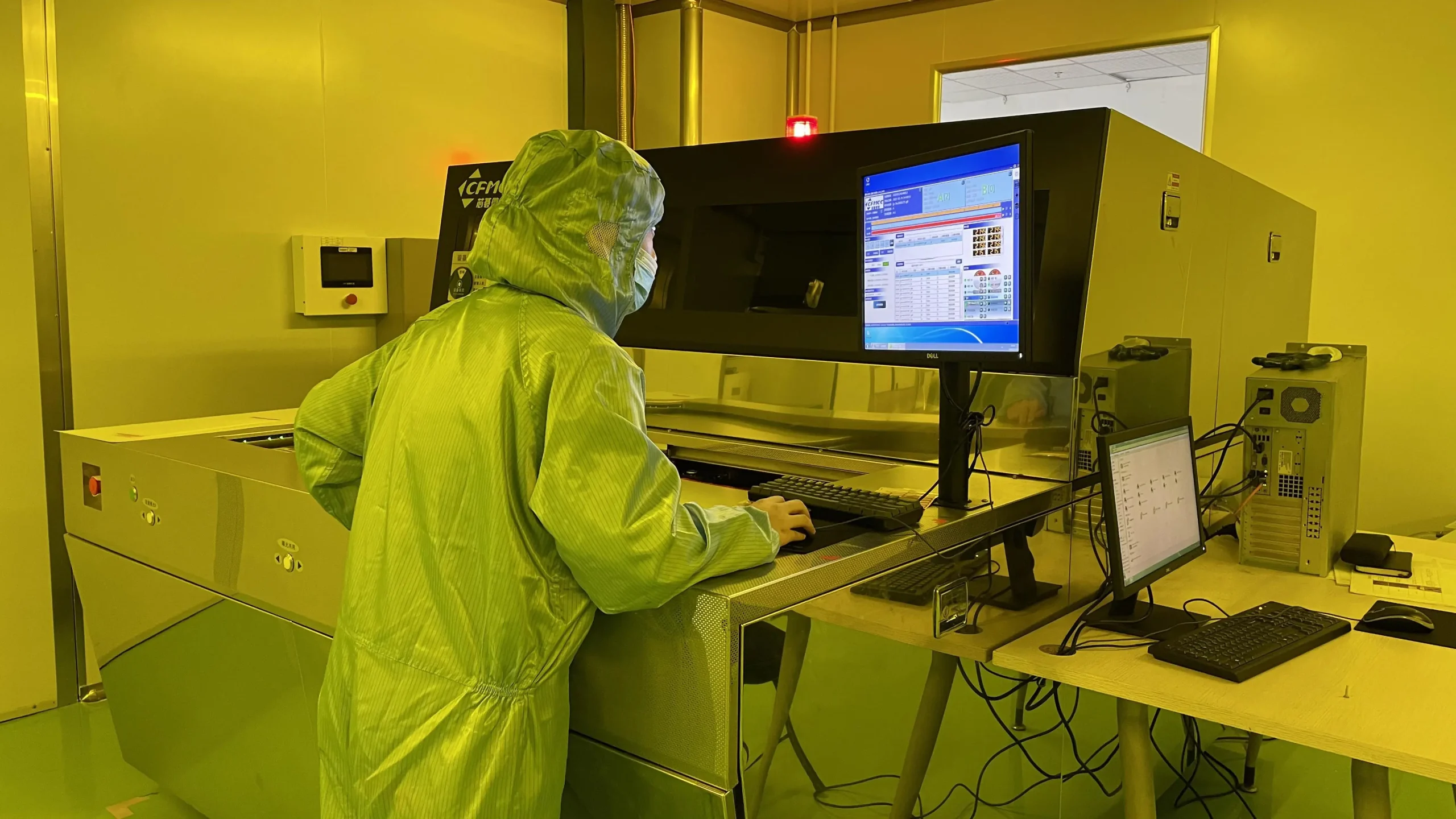
Commercial PCB assembly and aerospace PCB assembly use the same fundamental steps — paste printing, component placement, reflow soldering, and inspection. But the production environment they happen in, the process controls applied during assembly, and the inspection requirements after assembly are fundamentally different. Understanding these differences helps you evaluate whether a supplier’s aerospace claim is real or just a marketing statement.
Production Environment
In general PCB and commercial PCB assembly, the production floor is a standard industrial environment. Temperature and humidity are managed at a general level. ESD precautions are basic. Access to the production line is loosely controlled.
Aerospace PCB assembly requires a controlled environment at every point where a board is handled:
- ESD control is implemented to ANSI/ESD S20.20 standard. The floor is conductive. Ionizing air bars keep charge below ±50V. Every operator wears a wrist strap that is tested and logged daily. This matters because a single electrostatic discharge event can damage a component that passes all subsequent inspection but fails in the field months later.
- Humidity is maintained between 40% and 60% RH and logged continuously. Below 30% RH, static discharge risk increases. Above 60% RH, bare boards absorb moisture that causes solder joint defects during reflow.
- Moisture-sensitive components (BGAs, QFNs, fine-pitch ICs) are stored in dry cabinets and tracked for floor life per IPC/JEDEC J-STD-033. A component that exceeds its floor life must be baked before use. In commercial production, this is often managed informally. In aerospace, it is a documented process with traceability records.
- Access to the production line is restricted to trained, certified operators. Anyone handling an aerospace build must hold current IPC certification at the appropriate level.
Commercial production manages these factors to a degree. Aerospace production manages them to documented, auditable specifications — and any lapse is a nonconformance, not an oversight.
Production Process
The assembly process sequence is the same in both commercial and aerospace production. What is different is how tightly each step is controlled and what the line does when something is out of specification.
| Process Step | Commercial PCB Assembly | Aerospace PCB Assembly |
|---|---|---|
| Stencil aperture validation | Carried over from similar designs | Engineered and validated per paste type and component mix for each specific design |
| Solder paste printing atmosphere | Nitrogen optional; used selectively | Nitrogen purge standard on all builds to prevent premature alloy oxidation |
| Paste print failure response | Operator judgment; minor deviations passed | Hard stop — any out-of-spec pad triggers full wipe and reprint; no exceptions |
| SMT placement accuracy | ±50–75 µm typical | ±30 µm with fiducial-corrected vision verification on every BGA and fine-pitch package |
| Wrong component event | Rework and continue; logged as yield loss | Formal Non-Conformance Report generated; production holds until root cause is identified |
| Reflow profile | Set per board family; checked periodically | Locked per individual assembly design; every oven run generates a recorded time-temperature trace linked to the board serial number |
| Reflow atmosphere | Nitrogen optional | Nitrogen atmosphere standard on all aerospace reflow cycles |
| Through-hole soldering operators | Performed by available operators | Performed only by operators with current J-STD-001 IPC certification; records maintained and verified |
| Through-hole barrel fill | 75% minimum; sampled visually | 75% minimum verified on every board; cross-section verification at defined production intervals |
| Process deviation response | Informal correction; production continues | Documented NCR; production held until corrective action is reviewed and approved |
The underlying difference is this: commercial assembly is tuned to achieve acceptable yield at speed. Aerospace assembly is locked to a validated process specification — and any deviation from that specification stops the line until the cause is understood.
Production Inspection and Testing
After assembly, both commercial and aerospace PCBs go through inspection and testing. The difference is in the coverage rate, the tolerance levels applied, and the additional screening steps that aerospace requires but commercial production does not.
3D AOI — coverage and tolerance
Commercial production often runs 2D AOI, sometimes on a sample basis. Aerospace requires 100% 3D AOI on every board after every assembly stage. The 3D height data catches BGA component tilt and solder collapse that 2D AOI cannot detect. Any failure generates a formal rejection record before the board moves forward.
3D X-ray — mandatory for hidden joints
BGA solder balls, QFN thermal pads, and connector pins under component bodies cannot be seen with optical inspection. Commercial production may spot-check these with X-ray on first articles. Aerospace requires 100% 3D X-ray on every board that contains BGAs or other hidden joints. Void percentage is measured per IPC-7095D Class 3 limits — significantly more restrictive than Class 2. A supplier without 3D X-ray capability cannot verify BGA joint quality. That is a disqualifying gap for any aerospace program using area-array packages.
Electrical testing — 100% net coverage
Flying probe testing at 100% net coverage is the standard for aerospace builds regardless of volume. In commercial production, electrical test coverage is sometimes reduced on shorter runs to save time and cost. In aerospace, every net on every board is verified against the validated netlist.
Functional testing — under load
Commercial boards are often tested with a pass/fail check against basic electrical specifications. Aerospace boards are operated under simulated system conditions using a custom ATE program developed for that specific board. The board is exercised across its full operating voltage and temperature range before it is accepted.
Environmental Stress Screening — present in aerospace, absent in most commercial production
This is one area where aerospace production genuinely adds a step that commercial production typically does not include at all.
ESS subjects every production lot to accelerated stress to expose latent defects — marginal solder joints, weak component bonds, or semiconductor defects that passed all prior inspection but would fail in early service. A typical aerospace ESS program includes:
- Thermal cycling: -55°C to +125°C for 10 to 20 cycles minimum, stressing solder joints at CTE mismatch interfaces
- Burn-in: Boards operated under full electrical load at 85°C to 125°C for 24 to 168 hours
- Vibration screening: Random vibration per MIL-STD-810 to verify solder joint and coating integrity
Units that fail ESS are removed and investigated. Units that pass have moved through the infant mortality region of the reliability curve before they reach the customer.
Reliability Qualification Testing — Before Production Begins
ESS screens every production lot. Reliability testing is different — it qualifies the design itself before volume production is approved. It is performed once on qualification samples, and the results must be accepted before the program moves to full production.
The tests that are unique to this stage — not covered by ESS — include:
- Sustained high and low temperature operation: Boards run continuously at +85°C to +125°C and at -55°C for extended hours, verifying that performance holds across the full rated temperature range under real operating load
- Humidity and salt spray: 85% RH damp heat and salt fog exposure per MIL-STD-810, verifying conformal coating integrity and surface insulation resistance under marine or tropical conditions
- Radiation testing (space-grade only): Total Ionizing Dose (TID) and Single Event Effects (SEE) testing for satellite and space platforms, confirming that semiconductors maintain specified performance after cumulative radiation exposure in the target orbit
A design that passes this sequence proves the materials, stack-up, and assembly process are all capable of surviving the platform’s full service life. This is why aerospace qualification timelines are longer than commercial programs — not bureaucracy, but evidence.
Conformal coating — specified, not defaulted
Every aerospace assembly receives conformal coating after electrical testing. The type is defined in the assembly drawing — it is an engineering decision, not a production default.
| Coating Type | Operating Range | Best Use | Reworkable |
|---|---|---|---|
| Acrylic (Type AR) | -65°C to +125°C | General aerospace; most widely used | Yes |
| Silicone (Type SR) | -65°C to +200°C | High-temperature modules near heat sources | With difficulty |
| Polyurethane (Type UR) | -65°C to +125°C | Fuel and chemical exposure environments | With difficulty |
| Parylene (Type XY) | -65°C to +200°C | Space, satellite, munitions — CVD deposition | No |
After application, every board is inspected under UV light for coverage. Witness coupons are cross-sectioned at defined intervals to verify coating thickness per IPC-CC-830C.
The Production Record That Ties It All Together
Every process step in aerospace PCB assembly appends its result to a production record tied to the board’s serial number — component lot numbers and Certificates of Conformance, paste print measurements, reflow profile traces, AOI and X-ray results, electrical test data, ESS cycle records, and conformal coating batch details.
This record is not administrative overhead. When a board fails in the field — even years after shipment — this is where the failure investigation starts. It is what makes root cause analysis possible instead of guesswork.
What Inspection and Testing Protocols Are Non-Negotiable?
Inspection in aerospace PCB production is not a final quality gate. It is woven into every process step, so that defects are caught and corrected at the stage where they are cheapest to address — not discovered at functional test after the entire build cost has been committed.
A full aerospace inspection sequence covers 3D SPI before placement, 100% 3D AOI after reflow, 3D X-ray for BGA and hidden-joint verification, flying probe electrical testing, functional testing under load, ESS, and micro-section analysis for lot qualification. Every inspection result is documented, linked to the board’s serial number, and retained in the production record.
Micro-Section Analysis for Lot Qualification
Micro-section (cross-section) analysis is a destructive inspection method that examines via plating thickness, copper foil integrity, laminate bonding, and solder joint microstructure at the microscopic level. It is performed on witness coupons fabricated alongside production boards. Micro-section results provide the definitive verification that the fabrication process is operating within IPC-6012DS control limits — and it is the inspection method that quality auditors examine first when reviewing a manufacturer’s aerospace process documentation.
What Should You Look for When Selecting an Aerospace PCB Assembly and Manufacturing Partner?
The decision to partner with a specific aerospace PCB manufacturer carries consequences across the entire program lifecycle. The wrong selection creates qualification delays, supply chain gaps, and in the worst cases, boards that fail acceptance testing after a full production run.
These are the criteria that matter — not the marketing claims, but the verifiable technical and operational facts.
Verify the Certifications, Not Just the Claims
A current AS9100D certificate from an accredited third-party certification body is verifiable. The issuing body’s name and certificate number are publicly searchable. ISO 9001 alone does not qualify a manufacturer for aerospace work — AS9100D is the aerospace-specific requirement. Nadcap accreditation for soldering and assembly processes represents the highest independent process-specific validation available for special process manufacturing.
Confirm the In-House Capability Stack
A true one-stop PCB assembly and manufacturing provider — in-house fabrication, component sourcing, SMT assembly, through-hole assembly, testing, conformal coating, and box-build — reduces custody transfers in the supply chain. Each custody transfer is a potential traceability gap, a handling risk, and a quality escape opportunity. When a manufacturer fabricates and assembles under one quality management system and one roof, accountability is clear and documentation integrity is higher.
Confirm the Inspection Equipment
The presence of 3D SPI, 3D AOI, and 3D X-ray inspection is not optional for aerospace PCB assembly. These are process-enabling tools. A manufacturer who cannot demonstrate calibrated 3D X-ray inspection capability cannot verify BGA solder joint quality — and that is a disqualifying gap for any program that uses BGA or other area-array packages.
Evaluate Component Sourcing Discipline
For aerospace builds, every component must come from authorized franchised distributors or directly from component manufacturers. Gray-market and spot-market sourcing creates counterfeit risk that no inspection process can fully mitigate once a counterfeit component is built into an assembly. Documented counterfeit prevention procedures per AS5553, incoming certificate verification, and lot traceability to manufacturer batch records are the baseline requirement.
Confirm Scalability From Prototype to Volume
The same quality management system and process controls should govern both prototype and volume aerospace PCB assembly. A manufacturer with separate “prototype” and “production” tracks using different processes introduces qualification risk between the prototype that passed acceptance testing and the production units that were built differently. True process scalability means the five engineering verification units are assembled on the same qualified process line as the eventual production run of five hundred.
How IWDF Solutions Supports Aerospace and Defense PCB Programs
IWDF Solutions is a Shenzhen-based one-stop PCB manufacturing and assembly provider with over 20 years of production experience across aerospace, defense, automotive, medical, and industrial electronics. Our aerospace PCB assembly capability is built around the process controls, inspection infrastructure, and documentation systems that defense and avionics programs require — not retrofitted onto a commercial assembly line.
Our aerospace program capabilities include:
- PCB fabrication — multilayer rigid boards, rigid-flex PCBs, PTFE and Rogers high-frequency substrates, polyimide flex, and hybrid stack-ups built to IPC-6012DS requirements, from prototype quantities through full volume production
- PCB assembly — SMT and through-hole assembly executed to IPC-A-610 Class 3 and Class 3A workmanship standards, with nitrogen reflow soldering as the production standard for high-reliability builds
- Inspection infrastructure — 3D SPI, 3D AOI, and 3D X-ray inspection at every production stage, flying probe electrical testing on all low-to-medium volume aerospace builds, and full functional test development
- Conformal coating — acrylic, silicone, polyurethane, and Parylene coating applied and inspected per IPC-CC-830C specifications, with UV and cross-section verification
- Component sourcing — BOM management with authorized distributor sourcing, full lot traceability documentation, and component authentication for counterfeit-sensitive parts
- PCB reverse engineering and cloning — recovery of lost or incomplete documentation for legacy aerospace hardware, reconstruction of obsolete PCB designs, and production of replacement boards where original manufacturing data no longer exists
- Engineering DFM support — design for manufacturability review, stack-up optimization for controlled impedance, material selection consultation, and IPC-6012DS compliance review before fabrication begins
For aerospace and defense OEMs, system integrators, and procurement teams sourcing PCB assembly and manufacturing for defense and aerospace programs, IWDF Solutions offers the engineering depth and production infrastructure to support your program from initial prototype through volume production.
Send us your Gerber files, BOM, and program requirements for a detailed technical and commercial review.
Frequently Asked Questions
Q1: What is the difference between IPC-A-610 Class 3 and Class 3A for aerospace PCB assembly?
Class 3 defines the standard high-reliability acceptance criteria for aerospace and defense assemblies — no acceptable defects, continuous operation required. Class 3A is an enhanced addendum specifically for space and military avionics. It adds tighter BGA void percentage limits, coplanarity requirements under 50 µm, and stricter solder fillet height criteria per component class. Class 3A applies when the assembly specification specifically calls it out — typically for satellite electronics, military avionics, and missile systems.
Q2: Does a PCB manufacturer in China need ITAR registration to produce aerospace PCBs?
ITAR (International Traffic in Arms Regulations) is a U.S. export control regulation. It applies when a U.S. customer shares technical data — Gerber files, BOMs, fabrication drawings — that is controlled under the U.S. Munitions List (USML). ITAR registration is required of U.S.-based entities in the supply chain. Non-U.S. manufacturers are not registered with the DDTC, but they must receive any ITAR-controlled technical data through a properly licensed export from the U.S. customer. Many commercial aerospace and avionics programs do not involve ITAR-controlled data — the customer’s export compliance team makes that determination, not the manufacturer.
Q3: What is the IPC-6012DS addendum and when does it apply?
IPC-6012DS is an addendum to IPC-6012D that extends rigid PCB fabrication requirements for space and military avionics applications. It adds enhanced requirements for via barrel plating thickness (1.0 mil minimum vs. 0.8 mil under standard Class 3), tighter annular ring and hole registration tolerances, mandatory micro-section documentation at defined production intervals, and stricter requirements for blind via structural integrity under thermal cycling. It applies whenever the assembly drawing or purchase specification references it — this is contractually driven by the prime contractor.
Q4: What certifications should I require from an aerospace PCB assembly supplier in China?
At minimum, require a current AS9100D certificate from an accredited certification body (not a self-declared claim), evidence of IPC-A-610 CIS/CIT certified inspectors, and documentation of 3D SPI, 3D AOI, and 3D X-ray inspection capability in-house. For programs that ship into the DoD supply chain, MIL-PRF-31032 certification from the Defense Logistics Agency is required for the fabrication side. Ask to see the actual certificates with issuing body and expiry date, and verify them independently.
Q5: Can aerospace PCB assembly be performed in China at the same quality level as U.S. or European manufacturers?
Yes, with the right supplier selection. Certification bodies that audit AS9100D compliance apply the same standard globally — an AS9100D certificate issued to a Shenzhen manufacturer by a UKAS or DAkkS accredited body represents the same quality management system standard as one issued to a U.S. manufacturer. The equipment, process controls, and inspection methods are not geographically constrained. The key is verifying that the certification is real, current, and audited — and that the manufacturer’s actual production capability matches what the certificate covers.
Q6: What is environmental stress screening (ESS) and is it mandatory for aerospace PCB assemblies?
ESS is a production process that subjects completed assemblies to accelerated environmental stress — thermal cycling, burn-in under electrical load, and vibration — to expose latent manufacturing defects before the boards are shipped. It is not the same as qualification testing, which validates the design. ESS screens every production lot to remove units with marginal solder joints, weak component bonds, or latent semiconductor defects that would cause early field failures. Whether ESS is contractually mandatory depends on the program specification — but for flight-critical electronics, it is strongly advisable regardless of whether it is explicitly required.
Q7: What types of PCBs does IWDF Solutions manufacture for aerospace applications?
IWDF Solutions manufactures multilayer rigid PCBs, rigid-flex PCBs, high-frequency PCBs using Rogers and PTFE substrates, polyimide flexible circuits, heavy copper PCBs for power applications, and hybrid stack-up boards combining different substrate materials across layers. All aerospace fabrication is performed to IPC-6012DS requirements. We support both prototype and volume production runs and provide DFM review and material selection consultation as part of the pre-production engineering process.

