

Wrong material, wrong assembly standard, wrong partner — these three decisions cause more medical PCB project failures than anything else.
Medical PCB success in 2025–2026 depends on understanding the key trends driving design complexity (wearables, edge AI, miniaturization), recognizing the real challenges that cause compliance failures (material mismatch, assembly process gaps, traceability breakdowns), and making the right decisions on substrates, standards, stackup, assembly, and manufacturer selection before the first prototype is built.
Most articles about medical PCBs explain what they are. This one focuses on what you need to decide. Whether you are developing a new medical device, re-sourcing an existing product, or evaluating a manufacturing partner in China, this guide gives you the practical reference points to make informed decisions — not just general knowledge to read and forget.

What Trends Are Reshaping Medical PCB Design Right Now?
The medical PCB market is changing fast. If your design process has not changed in the last two years, you are already behind.
The medical electronics market is on a serious upward trajectory. According to data from March 2025, the global medical PCB sector was worth $1.45 billion last year and is expected to climb to $2.45 billion by 2033. If you look at the bigger picture—including full diagnostic assemblies—that figure could soar as high as $9 billion. This isn’t just about more volume; it’s about a fundamental shift in tech. Across all major forecasts, three growth drivers are consistent: the rapid expansion of wearable diagnostic devices, the integration of edge AI into portable medical hardware, and tightening global regulatory standards that raise the compliance bar for every component in a regulated medical device — including the PCB.
Trend 1: Wearables Are Now a Medical-Grade PCB Category of Their Own
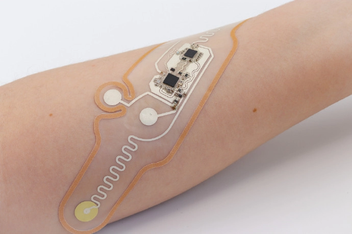
Wearable medical devices used to mean a fitness tracker with a heart rate sensor. Today they include 14-day cardiac patch recorders, continuous glucose monitors, non-invasive blood pressure wearables, and neural stimulation patches. These are FDA-regulated, Class II or Class III devices — not consumer products.
The PCB inside a medical wearable must meet requirements that did not exist five years ago:
- Fit within a footprint measured in square centimeters, often under 5 grams total device weight
- Survive 7 to 30 days of continuous skin contact and exposure to sweat
- Maintain at least IP67 waterproofing in a flexible, body-conforming form factor
- Operate on a battery small enough to be worn invisibly, while processing microvolt-level physiological signals
This has made rigid-flex PCBs the dominant architecture for medical wearables. A rigid-flex design eliminates mechanical connectors — the most common failure point in portable assemblies — and achieves up to 40% size reduction compared to traditional rigid boards with cable harnesses. High-quality medical rigid-flex designs are rated for 100,000+ bend cycles without mechanical fatigue.
Trend 2: Edge AI Is Directly Changing PCB Layout Requirements
The shift toward on-device AI inference is not just a software trend. It changes the PCB.
Arrhythmia detection, continuous SpO₂ trend analysis, and predictive glucose forecasting are now running on the wearable device itself — not in the cloud. This requires MCUs equipped with neural processing units (NPUs), LPDDR memory running at gigahertz-level interfaces, BLE 5.3 transceivers, and multi-channel ADC front-ends. All of this must coexist on a miniaturized HDI board.
PCB designers handling medical wearable projects in 2026 are dealing with multi-GHz signal integrity, high-speed memory routing, and ultra-low-power management simultaneously — in a sub-40 mm² footprint. That is a materially more complex design problem than anything the same device category required three years ago.
Trend 3: Regulation Is Getting Stricter, Not Easier
EU MDR 2017/745 is fully in force. The FDA’s 2023 cybersecurity guidance for connected devices has added hardware security requirements. IPC is developing dedicated medical device addendums (IPC-6012DM and IPC-6013DM) that go beyond existing Class 3 standards.
The practical impact: a PCB that would have passed regulatory review two years ago may not pass today. If your medical PCB design was frozen before 2024 and your device connects to any network or Bluetooth stack, your hardware design likely needs a cybersecurity review — including evaluation of whether a hardware security module is required on the PCB itself.
These trends set the context. But knowing the trends is only useful if you also know where things go wrong. That is where the challenges come in.
What Makes Medical Device PCB Design So Hard to Get Right?
Most medical PCB design failures are not caused by difficult technology. They are caused by common errors made at predictable decision points — and caught at the worst possible time.
The hardest part of medical device PCB design is not the circuit itself. It is the gap between a design that works in simulation and a design that survives regulatory submission, biocompatibility testing, EMC compliance testing, and ten years of clinical use. That gap is where most projects lose time and budget.
The Five Design Errors That Cause the Most Project Delays
Understanding where medical PCB design typically fails is more useful than a generic best-practice list. These five errors are the ones that consistently send projects back to the redesign phase.
| Design Error | When It Is Discovered | Typical Cost |
|---|---|---|
| EMI/EMC failure due to poor stackup and ground plane design | At EMC test, after design lock | 3–6 month delay, full board respin |
| Incorrect impedance specification for diagnostic signal channels | During signal validation or calibration | Redesign plus re-validation under ISO 13485 |
| Missing ISO 10993 biocompatibility testing for coating or substrate | At regulatory submission stage | 8–12 week test cycle added to timeline |
| Via-in-pad errors and DFM issues found after first production build | During production yield review | Change control documentation, re-validation |
| No hardware redundancy on life-critical signal paths | In risk management review or field testing | Architectural redesign required |
EMI is a design-phase decision, not a test-phase fix.
A hospital environment is one of the densest RF environments in the world — Wi-Fi access points, cellular systems, surgical navigation equipment, CT scanners, and dozens of portable monitors operate in the same room simultaneously. IEC 60601-1-2 exists specifically because a medical device that radiates interference can disrupt other equipment, and a device that is susceptible to interference can produce wrong readings at the moment they matter most.
Passing IEC 60601-1-2 starts in your layer stackup. Every high-speed signal layer must be sandwiched between continuous ground planes. Ground plane continuity must be maintained — any slot or discontinuity becomes a radiating structure. Differential pairs for ECG and EEG signal lines must hold 100-ohm impedance consistently. Board-level EMI shields must be soldered over RF-sensitive sub-circuits before the first prototype is tested.
These decisions cannot be made after an EMC test failure. At that point, every fix requires a formal design change under your QMS.
Impedance control is a fabrication specification, not a guideline.
For ECG, EEG, and SpO₂ boards, ±1% impedance accuracy across differential measurement channels is required to prevent physiological signal distortion. This is not a preference. It must be specified in the fabrication order. The fabricator must return a TDR (time-domain reflectometry) verification report before you accept the boards. If your current fabricator does not provide TDR reports for medical orders, that alone tells you something important about their experience level.
ISO 10993 testing has a fixed timeline that cannot be compressed.
A complete biocompatibility test panel under ISO 10993 takes 8 to 12 weeks. If this requirement is identified at the regulatory submission stage rather than the design stage, it cannot be parallel-tracked with other activities — it simply adds 8 to 12 weeks to your schedule. The fix is to identify any patient-contact risk for PCB materials, solder mask, or conformal coatings at the start of the design phase and initiate testing immediately.
Now that we have mapped the design challenges, the next major area of risk is in the assembly itself — where even a well-designed PCB can fail if the manufacturing process is not calibrated to medical standards.
Why Does Medical PCB Assembly Fail — and How Do You Prevent It?
A well-designed medical PCB assembled on a commercial production line will eventually fail. The design is not the problem. The process is.
More than 40% of medical device companies report production delays or field failures caused by PCBA non-compliance or assembly process deficiencies. IPC Class 3 assembly is not the same as commercial assembly with extra inspection. It is a different process, run by differently trained operators, to different acceptance criteria, with documentation that a regulatory auditor can trace from raw material to finished unit.
What IPC Class 3 Medical PCB Assembly Actually Requires?
| Assembly Stage | Medical Class 3 Requirement | Why It Matters |
|---|---|---|
| Solder paste printing | SPI (solder paste inspection) after every print run | Paste volume variation causes opens and bridges that AOI misses |
| Component placement | ±0.05 mm maximum offset for fine-pitch BGA | 0.1 mm misalignment at 0.4 mm pitch BGA creates shorts or opens |
| Reflow soldering | Nitrogen-assisted reflow, validated thermal profile, J-STD-001 Class 3 | Prevents oxidation; controls voiding in fine-pitch solder joints |
| Post-reflow AOI | 3D AOI, 100% of boards, no skip-lot | Catches fillet geometry, tombstoning, and bridging |
| BGA and QFN inspection | In-house X-ray (AXI), 100% of boards | BGA joints are invisible to optical inspection |
| BGA void acceptance | Individual ball voids below 15%; cumulative below 20% | Voids create thermal resistance that accelerates long-term fatigue failure |
| Traceability records | Component lot → board serial number, fully documented | Required for FDA DHR and ISO 13485 audit compliance |
The BGA void requirement deserves attention. IPC Class 3 sets a maximum of 25% individual void per ball. Medical assembly practice tightens this to below 10% — because solder voids in life-critical assemblies introduce thermal resistance that drives long-term fatigue failure in devices expected to operate for 10+ years.
The only way to verify BGA solder quality is X-ray inspection. Ask your assembler directly: Is X-ray performed in-house or outsourced? What is the system resolution? What format is used for void analysis reports? A manufacturer that cannot answer these questions immediately does not run a genuine Class 3 medical assembly line.

Conformal Coating: Where Assembly and Biocompatibility Meet
Conformal coating is not a finishing step. For Class III implantable devices, it is a regulatory requirement with documented validation.
Parylene is the standard for implantable medical PCBs. It is applied by vapor deposition polymerization — a process that coats every exposed surface uniformly, including the undersides of low-clearance components, the interiors of via holes, and the sharp edges of solder joints that liquid coatings cannot reliably reach.
Key properties that make parylene the right choice for implantable assemblies:
- USP Class VI certified, ISO 10993 compliant — no cytotoxicity, no tissue reaction
- Pinhole-free at micron-level thickness — complete dielectric isolation without added weight
- Survives autoclaving, gamma radiation, and EO sterilization without degradation
- Impervious to bodily fluids, acids, and organic solvents over the full device service life
Parylene C is specified for most cardiac implants. Parylene HT offers improved long-term stability under continuous physiological fluid exposure and is preferred for neural devices where the coating must remain stable for 10+ years in a biologically active environment.
If your device will have any patient-contact or implantable component, specify parylene in your assembly requirements before PCB layout begins. Adding it after the first build requires re-validation of the complete assembly.
Which Materials and Standards Are Non-Negotiable for a Medical PCB?
Choosing a substrate based on cost rather than application requirements is one of the most common and most expensive decisions in medical PCB development.
The substrate and coating specification for a medical PCB is set by device class and application frequency — not by budget preference. For Class II and Class III devices, the material selection directly affects biocompatibility compliance, EMC performance, signal fidelity, and long-term reliability. Getting it wrong at the design stage means getting it wrong permanently.
Substrate Selection by Device Application
| Substrate | Key Properties | Best-Fit Medical Application |
|---|---|---|
| FR-4 Tg170+ | Good thermal stability, cost-effective, proven process | Class I/II control boards, power modules, non-patient-contact hardware |
| Polyimide | Stable -200°C to +400°C, chemically inert, flexible | Flex PCBs, wearable probe interconnects, implantable assemblies |
| Rogers RO4350B | Low loss tangent, stable dielectric constant up to 20 GHz | Ultrasound transducer signal layers (1–20 MHz), high-frequency imaging |
| Taconic RF-35 | Consistent Dk, low dielectric loss, proven RF performance | RF telemetry boards, diagnostic imaging front-ends |
| Ceramic (Al₂O₃/AlN) | Exceptional thermal conductivity, dimensionally stable | High-power ultrasound front-ends, implantable high-density assemblies |
The material decision tree for most medical PCBs follows three questions:
1. Does the device operate above 1 MHz signal frequency?
If yes, FR-4 is likely insufficient. Diagnostic ultrasound, RF telemetry, and high-speed biosensor ADC front-ends all require a low loss tangent and stable Dk across the operating temperature range. Rogers and Taconic laminates are the standard for these applications.
2. Does the PCB have any patient-contact or implantable risk?
If yes, standard FR-4 solder mask and commercial conformal coatings are not acceptable without ISO 10993 testing documentation. Polyimide substrates with parylene coating are the baseline for implantable designs.
3. What is the device class?
Class III devices require biocompatible materials, full IPC Class 3 fabrication and assembly, J-STD-001 Class 3 soldering, and serial-level traceability throughout production. Class I devices can use standard FR-4 with general IPC compliance. Class II falls between these two extremes depending on specific device application and risk profile.

The Standards Every Medical PCB Project Must Address
Knowing which standards apply to your project before design begins prevents the most common regulatory surprises.
| Standard | Scope | Who It Applies To |
|---|---|---|
| ISO 13485:2016 | QMS for medical device design and manufacturing | Manufacturer and design partner |
| FDA 21 CFR Part 820 | Quality System Regulation for US-market devices | Manufacturer for Class II/III devices sold in USA |
| IEC 60601-1 | General safety for medical electrical equipment | Any powered medical device |
| IEC 60601-1-2 | EMC requirements for hospital environments | Any connected or electrically active medical device |
| IPC-A-610 Class 3 | Assembly acceptance criteria | PCBA manufacturer |
| J-STD-001 Class 3 | Soldering process requirements | PCBA manufacturer |
| ISO 10993 | Biocompatibility for patient-contact materials | Any device with patient-contact PCB material or coating |
| IEC 62304 | Software lifecycle | Devices with embedded software |
One standard that is often overlooked until it’s too late: IEC 62304. It governs the software development lifecycle for medical device firmware. The FDA’s 2023 cybersecurity guidance adds hardware-level requirements on top of this — including on-board hardware security modules (HSMs) and FIPS-compliant cryptographic functions for connected Class II and Class III devices. These are PCB design decisions, not software decisions. They need to be on the schematic before layout begins.
How Do You Choose and Evaluate a Medical PCB Manufacturer?
Every PCB factory in Shenzhen claims to serve the medical market. Very few can prove it with documentation.
The difference between a qualified medical PCB manufacturer and a commercial shop doing medical work is visible in three places: their ISO 13485 certificate scope, their in-house inspection equipment, and their traceability documentation system. If any of these three are absent or incomplete, the compliance risk falls entirely on you as the device developer.
What to Verify Before You Place a Medical PCB Order?
Do not start with a price request. Start with capability verification. Use this checklist:
| Verification Area | What to Request | What to Watch For |
|---|---|---|
| ISO 13485:2016 certification | Certificate plus written scope statement | Scope must explicitly cover assembly, not just bare board fabrication |
| IPC-A-610 Class 3 | Process certification and inspector credentials | Confirms assembly team is trained to medical acceptance criteria |
| J-STD-001 Class 3 | Soldering process qualification records | Must include nitrogen-assisted reflow and validated thermal profiles |
| X-ray inspection | Confirm in-house AXI with resolution specification | BGA and QFN joints cannot be verified any other way |
| Traceability system | Request a sample work order document | Must show component lot traceability to finished board serial number |
| DFM review process | Request a sample DFM report from a previous project | Should identify via-in-pad, thermal relief, and pad geometry issues |
| ISO 10993 data | Coating material biocompatibility certificates | Required for any patient-contact or implantable coating material |
| TDR impedance reports | Sample impedance verification report | Must confirm ±1% impedance accuracy is achievable and documented |

One-Stop vs. Split-Source: A Decision That Affects Compliance, Not Just Cost
Many medical device OEMs split PCB fabrication and assembly between different suppliers to reduce unit cost. The unit cost saving is real. The compliance risk is also real — and it is often underestimated.
When fabrication and assembly are done by different companies, no single entity owns the complete Device History Record. A material substitution in the bare board may not trigger re-validation at the assembly level. A process change at the fabricator may not reach the assembler’s documentation system. If the FDA audits your production records, the gap between supplier A’s records and supplier B’s records is your problem.
A single ISO 13485-certified manufacturer handling design, fabrication, and assembly under one quality system eliminates this gap. The same engineering team that reviews the schematic and produces the Gerber files also defines the stencil apertures, validates the reflow profile, performs AOI and X-ray inspection, and documents the complete production record in a single traceable Device History Record.
For Class III devices, a split-source model is a genuine compliance risk. For Class II devices, the documentation overhead of managing two separate quality systems often costs more than the unit price savings.
What a Full-Service Medical PCB Partner Should Actually Provide?
Beyond certifications, a genuine medical PCB partner should offer:
- Integrated DFM and DFT review before any production release — catching via-in-pad errors, pad geometry issues, and stencil aperture ratios before design lock, not after the first failed build
- Signal integrity and EMC simulation capability — the ability to model impedance, identify crosstalk risks, and flag EMC concerns before fabrication
- Prototype-to-volume transition under the same quality system — not a separate process for prototypes and another for production
- Conformal coating validation with documented process records for parylene, acrylic, or silicone as required by device class
- Component traceability from incoming material lot through to shipped finished board — with records formatted for FDA DHR compliance
IWDF Solutions, based in Shenzhen with over 20 years of engineering experience, provides exactly this one-stop service model. Its capabilities span medical PCB design (up to 32-layer stackup, HDI, rigid-flex, controlled impedance), PCB reverse engineering, prototype and volume PCBA production with IPC Class 3 process controls, in-house AOI and X-ray inspection, and full conformal coating application with process documentation. For overseas medical device OEMs who need a single partner with traceable quality systems from design to delivery, IWDF Solutions provides direct engineering engagement rather than intermediary sourcing.
What Key Considerations Apply Specifically to Custom Medical PCB Projects?
Custom medical PCB projects fail for predictable reasons. Knowing them in advance changes how you plan your program.
The most common reason custom medical PCBs miss regulatory submission deadlines is not technical complexity — it is planning failures that compress validation timelines, trigger late-stage redesigns, or produce documentation gaps that cannot be closed retroactively. These are avoidable with the right decisions early.
Device-Class-Specific Design and Production Considerations
| Device Class | Design Considerations | Assembly Considerations | Documentation Considerations |
|---|---|---|---|
| Class I | Standard FR-4 acceptable; general DFM review | IPC Class 2 acceptable minimum; basic inspection | Basic production records; no DHR required |
| Class II | Controlled impedance; IEC 60601-1-2 EMC design; DFM + DFT mandatory | IPC-A-610 Class 3; 100% AOI; functional test | Batch-level traceability; 510(k) supporting records |
| Class III | Biocompatible substrate; parylene coating; ISO 10993 test data; hardware redundancy on life-critical paths | IPC Class 3; in-house X-ray; BGA void <10%; nitrogen reflow; conformal coating validation | Serial-level lifetime traceability; full DHR; UDI labeling |
Three Planning Decisions That Protect Your Timeline
1. Lock substrate and coating specification before schematic capture begins.
The material specification determines whether your PCB can pass ISO 10993 testing, meet EMC requirements, and survive the device’s intended sterilization method. A material change after schematic capture triggers a design change under your QMS. A material change after first prototype triggers re-validation. Neither is recoverable without schedule impact.
2. Start ISO 10993 testing at the same time as PCB layout.
Biocompatibility testing takes 8 to 12 weeks and cannot be compressed. If your device has any patient-contact risk for PCB materials or conformal coatings, initiate ISO 10993 testing the week your PCB layout begins. This parallel-tracks testing with design completion and prevents it from becoming a critical path item at the regulatory submission stage.
3. Define your traceability requirements before selecting your manufacturer.
FDA requirements for implantable devices mandate lifetime traceability. For non-implantable Class II devices, records must be maintained for at least two years after product discontinuation. Your manufacturer’s traceability system must be compatible with these requirements before you place your first production order. Retrofitting traceability documentation after production has started is extremely difficult and creates audit exposure.
FAQ: Medical PCB Design and Assembly
Q: What is the difference between a medical PCB and a standard PCB?
A medical PCB must meet failure rates below 0.1% over 10+ years, 100% board-by-board IPC Class 3 inspection, full component traceability from raw material to shipped unit, and in many cases biocompatible materials and coatings. Standard commercial PCBs do not carry these requirements. The difference is enforced by ISO 13485, FDA 21 CFR Part 820, and IEC 60601-series standards.
Q: What certifications should a medical PCB manufacturer hold?
At minimum: ISO 13485:2016 with a scope that covers both fabrication and assembly (not fabrication only), IPC-A-610 Class 3 and J-STD-001 Class 3 process certifications, RoHS/REACH material compliance documentation, and ISO 10993 data for any conformal coatings used on patient-contact or implantable designs.
Q: What PCB type is best for medical wearable devices?
Rigid-flex PCBs are the dominant architecture for medical wearables. They eliminate mechanical connectors (the primary failure point in portable assemblies), achieve up to 40% size reduction compared to rigid boards with cable harnesses, and are rated for 100,000+ bend cycles. For high-density wearable designs, 8+ layer HDI rigid-flex is the standard architecture in 2025–2026.
Q: What is parylene coating and when is it required for medical PCBs?
Parylene is a conformal coating applied by vapor deposition polymerization. It forms a pinhole-free, chemically inert, biocompatible film over every surface of a PCB assembly, including areas that liquid coatings cannot reach. It is USP Class VI certified and ISO 10993 compliant. Parylene is required for Class III implantable devices and is specified for any PCB with direct patient-contact risk where standard conformal coatings cannot meet biocompatibility requirements.
Q: How does device classification affect the PCB design and assembly process?
Class I devices need general IPC compliance and basic traceability. Class II devices require IPC Class 3 assembly, IEC 60601-1-2 EMC compliance, controlled impedance, and batch-level traceability. Class III devices require biocompatible substrates, parylene coating, ISO 10993 testing, full IPC Class 3 process controls with in-house X-ray inspection, and serial-level lifetime traceability. The classification affects material selection, assembly standards, inspection requirements, and documentation obligations simultaneously.
Q: Can a Chinese medical PCB manufacturer meet FDA and EU MDR compliance requirements?
Yes — provided the manufacturer holds ISO 13485:2016 certification with a scope that covers design, fabrication, and assembly; operates IPC Class 3 assembly processes with documented process controls; and maintains a traceability system compatible with FDA DHR and EU MDR technical documentation requirements. China accounts for over 50% of global PCB production capacity, with Shenzhen as the primary hub for high-complexity medical PCB manufacturing. Cost advantages are substantial — complex Class II PCBA production costs are typically 60–75% lower than equivalent North American or European manufacturing — without requiring any compromise on compliance standards when the right manufacturer is selected.
Q: What is the most common reason medical PCB projects miss their regulatory submission deadlines?
The most common cause is that ISO 10993 biocompatibility testing is identified too late in the program. A full ISO 10993 test panel takes 8 to 12 weeks and cannot be expedited. Projects that identify this requirement at the submission stage rather than the design stage add this time directly to their critical path. The second most common cause is EMC failure after design lock — requiring a board respin and re-validation that typically adds 3 to 6 months to the schedule.

