

Your wearable device project needs to fit inside a housing smaller than a matchbox, run for days on a single charge, and never hurt the patient wearing it. Most first-pass designs fail on at least one of those three.
Medical wearable PCB design requires three engineering priorities working together: an HDI stack-up compact enough for a body-worn enclosure, a power architecture that supports multi-day sensor operation without sacrificing clinical accuracy, and materials that satisfy ISO 10993 biocompatibility evaluation at every patient-contact layer. Failing any one of these blocks regulatory approval and forces costly redesigns before the device reaches its first clinical trial.
This article examines each of those constraints in engineering depth — layer stack-up logic, material selection, power architecture, signal conditioning, biocompatibility choices, regulatory compliance, and the manufacturing factors that determine whether a design survives from prototype to high-volume production. It is written for hardware engineers, product managers, and procurement leads who are evaluating custom PCB design for medical devices and need a qualified manufacturing partner in China.

Why Does Miniaturization in Medical Wearable PCB Design Demand More Than Just Smaller Components?
Miniaturizing a medical wearable requires a lot more than just a tight layout with smaller components. If you simply switch to smaller parts and place them closer together on a conventional stack-up, you sacrifice the electrical integrity of your reference planes. Analog traces lose their controlled return path, allowing digital switching noise to bleed directly into critical sensor signals. By moving to HDI architecture and using laser-drilled microvias, we can maintain dedicated signal separation and controlled impedance, achieving medical-grade accuracy at a fraction of the size.
How HDI Technology Changes What Is Physically Possible
Standard PCB fabrication uses mechanically drilled through-holes with a minimum diameter of around 0.3 mm. HDI fabrication uses laser drilling, reaching via diameters as small as 0.075 mm. Trace widths drop from 100 µm on standard boards to 25 µm on HDI. Those two numbers together are what make it possible to route a 0.5 mm-pitch BGA on a board small enough to wear on a wrist.
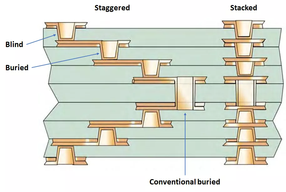
HDI also introduces blind and buried vias — connections that travel only partway through the stack-up, or only between internal layers. This frees surface area for component placement that through-hole vias would otherwise consume. The result is component densities that standard 4-layer PCBs simply cannot approach at the same footprint.
A 6-Layer Stack-Up Built for Clinical Wearable Use
The 6-layer stack-up is the standard architecture for wearable vital-signs monitors in the 40–80 mm form factor. Each layer has a specific function — this is not interchangeable with a generic 6-layer stack from an industrial product.
| Layer | Function | Key Design Rules |
|---|---|---|
| L1 — Top | Component placement | BGA at 0.5 mm pitch; optical sensors; BLE antenna integration zone |
| L2 | Mixed-signal routing | Analog traces guarded and kept separate from digital buses |
| L3 | Ground plane | AGND/DGND boundary defined here; thermal vias connect downward |
| L4 | Power distribution | Independent copper fills: 3.3 V digital, 1.8 V analog, RF supply |
| L5 | Secondary signal routing | Low-speed digital, I²C, battery management connections |
| L6 — Bottom | Return-path plane | Continuous copper for EMI suppression; bottom-side components |
IWDF Solutions applied this architecture to a German medtech client’s wearable vital-signs monitor. The project required optical pulse oximetry, ECG front-end, body temperature sensing, BLE 5.2 connectivity, and battery management — all inside a 55 mm × 40 mm housing. The final PCB measured 54 mm × 38 mm × 1.6 mm. The design used buried via technology for inter-layer routing, 4 mil trace/space throughout, 0.5 mm pitch BGA placement, and an integrated on-board antenna that eliminated the external antenna component entirely. First-pass manufacturing yield reached 97.8%.
Rigid-Flex: The Architecture for Patch and Contour-Following Wearables
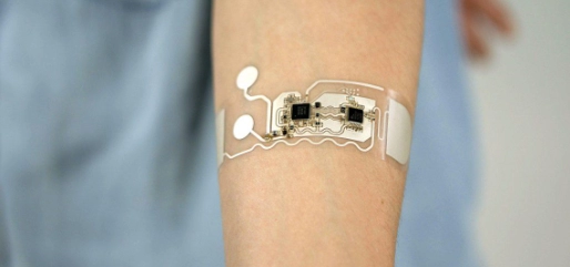
Not every wearable sits flat on a wrist. Continuous glucose monitors, cardiac event patches, and rehabilitation sensors must conform to curved body surfaces. For these applications, rigid-flex PCBs solve the structural problem. They combine FR-4 rigid sections — which carry dense ICs, connectors, and BGAs — with polyimide flexible tails that bend to fit the enclosure geometry.
Rigid-flex designs reduce board footprint by roughly 40% compared to a split-rigid-board-and-cable approach. Quality flex sections sustain over 100,000 bend cycles, which is a practical requirement for a device worn through daily movement and sleep.
Flex zone layout rules differ from rigid PCB rules in several specific ways:
- Conductors in flex zones must run parallel to the bend axis — perpendicular routing fatigues and cracks the conductor
- Minimum bend radius: ≥ 5× total flex thickness for static bends; ≥ 10× for dynamic flex zones
- No through-hole vias in flex zones — blind laser-drilled vias only
- Copper teardrops at every rigid-to-flex interface act as strain relief to prevent delamination at stress concentration points
Once the stack-up and flex architecture are defined, the next decision layer is material selection — and this is where most medical wearable projects encounter their first regulatory surprise.
Which PCB Substrate and Stack-Up Materials Actually Work for a Body-Worn Medical Device?
Some teams default to FR-4 because it’s familiar and budget-friendly, but for a medical wearable in constant skin contact, it’s usually the wrong choice. FR-4 falls short in three critical areas: it lacks the flexibility needed for skin-adjacent zones, its standard solder mask isn’t biocompatible, and its HASL finish can’t handle the fine-pitch BGAs that modern sensors require.
For body-worn tech, the professional standard is Polyimide for flexibility, ENIG for precise assembly, and specialized coatings like Parylene C or silicone for the finished board. FR-4 should be strictly limited to internal rigid layers with zero patient contact. Even then, you’ll need full ISO 10993 documentation ready before you even think about a regulatory submission.
The Four Material Decisions and What to Specify for Each
These four choices must be made before layout begins. Changing any of them after routing is complete typically forces a new board spin.
1. PCB substrate — match the material to the contact zone
| Zone | Correct Material | Why |
|---|---|---|
| Internal rigid layers, no skin-contact pathway | FR-4 | Cost-effective; acceptable with ISO 10993 documentation |
| Flex zones with continuous skin contact | Polyimide (PI) — ISO 10993-5 certified grade | Chemically inert; flexible; cytotoxicity certificate available from qualified laminate suppliers |
| RF sections at 2.4 GHz (BLE antenna) | PTFE or Rogers-series PTFE composite | Stable dielectric constant (Dk) across temperature; low loss tangent at high frequency |
| High thermal load or implant-adjacent areas | Ceramic substrate | Maximum chemical inertness; thermal conductivity far above FR-4 |
2. Solder Mask: Don’t Trust the “Green Oil”
A common trap is assuming that standard green solder mask is safe because it’s “just plastic.” In reality, most standard masks haven’t been tested for skin irritation.
- The Pro Move: Don’t take the supplier’s word for it. Request their Cytotoxicity Test Data. Reliable medical PCB partners keep this as a one-page conformance document and will provide it upon request.
- The Standard: Specify IPC SM-840 Class T as your minimum requirement.
3. Surface Finish: Why ENIG is King (and the Nickel Exception)
ENIG (Electroless Nickel Immersion Gold) is the standard for medical PCB assemblies because of its surface flatness. ENIG holds ±2 µm versus ±10–20 µm for lead-free HASL. At 0.4–0.5 mm BGA pitch — standard for modern BLE SoCs and AFE chips — that flatness difference determines whether solder joints form reliably or fail under the first thermal cycle.
| Surface Finish | Flatness | Fine-Pitch BGA Support | Shelf Life | Skin-Contact Use |
|---|---|---|---|---|
| ENIG | ±2 µm | Excellent | 12–18 months | Yes — nickel-free variant for direct skin contact |
| Lead-Free HASL | ±10–20 µm | Poor | 6–12 months | Not recommended |
| OSP | Flat | Good | 3–6 months | Single-use disposable devices only |
| Hard Gold | Flat | Excellent | 24+ months | Yes — preferred for ECG electrode contact pads |
The one exception: nickel is a common contact allergen. For any electrode pad or conductive surface that touches skin directly — ECG contacts, impedance measurement pads — specify nickel-free ENIG or hard gold plating. This is a layout-stage decision; specifying it as a production note after routing is complete adds cost and sometimes forces pad geometry changes.
4. Conformal coating — the outer layer that determines biocompatibility and moisture protection
The coating is the “outer skin” of your PCB. It determines both moisture protection (from sweat) and final biocompatibility.
- Medical-Grade Silicone: Best for high-flex zones. It’s softer and more “rubbery,” allowing the board to flex repeatedly without the coating cracking.
- Parylene C: The “gold standard” for wearables. It’s incredibly thin, pinhole-free, and offers elite protection for devices in continuous skin contact.
With substrate, solder mask, surface finish, and coating defined, the next decision layer is power architecture — and it starts at the PCB, not in firmware.
What Power Management Architecture Keeps a Medical Wearable Running for Days Without Sacrificing Accuracy?
A clinical wearable that runs out of battery after 16 hours fails its clinical purpose. Most power depletion problems in wearables trace back to PCB layout decisions, not firmware optimization gaps.
Medical wearable power management requires a PMIC with dynamic voltage scaling and standby quiescent current below 0.5 µA, complete separation of analog and digital power planes at the layout level, hardware load switches on every peripheral domain, and an MCU sleep current target of ≤ 1 µA. Achieving these targets is a PCB architecture problem before it is a firmware problem.
The Three Layers Where Power Efficiency Is Determined
Power optimization in a medical wearable works at three layers simultaneously. Firmware can only optimize within the headroom that the PCB layout creates.
Layer 1 — PMIC selection
Modern PMICs achieve voltage conversion efficiency above 90%, compared to 70–80% for older or poorly matched regulators. For medical wearables, the features that matter most are:
- Dynamic voltage scaling: reduces MCU core supply by 20–30% during idle periods
- Quiescent current in standby: below 0.5 µA at idle is achievable with current-generation devices
- Independent regulated rails: one each for the analog front-end (1.8 V), digital logic (3.3 V), and RF subsystem
- Integrated battery fuel gauge: essential when a patient-worn device cannot simply be recharged on demand
Layer 2 — PCB layout decisions that directly affect power consumption
| Layout Decision | Effect on Power and Noise |
|---|---|
| Separate analog and digital power planes | Blocks PMIC switching transients from entering the AFE supply rail |
| 100 nF decoupling capacitors within 0.5 mm of each power pin | Suppresses transient load spikes before they reach sensor circuits |
| Short, wide power traces throughout | Reduces IR drop; less energy dissipated as resistive heat |
| Thermal via arrays directly under PMICs and regulators | Prevents thermal derating events that increase quiescent losses |
| Hardware load switch on every peripheral power domain | Allows the MCU to fully cut power to idle subsystems between measurement cycles |
Layer 3 — Sampling architecture and power gating
Every biosensor sampling event activates the LED drivers, AFE, ADC, and MCU processing pipeline. Basic heart rate monitoring runs at 5–10 Hz. Accurate heart rate variability analysis requires 100–200 Hz. Each factor-of-ten increase in sampling rate creates a cascading load across the entire signal chain. The PCB must support complete hardware power gating between cycles — not just software sleep modes that leave power rails energized. That means a dedicated load switch IC on every peripheral domain, controlled by MCU GPIO. It is a layout decision, and it must be made before routing begins.
Achieving ≤ 1 µA MCU Sleep Current in a Real Production Design
This target is achievable on current-generation BLE SoCs. But the PCB has to support it. An MCU cannot reach ≤ 1 µA sleep current if the PCB leaves unused rail sections energized through shared LDO connections, or if leakage paths exist through pull-up resistors on peripheral I/O lines.
The layout requirements:
- Individual load switches on every switchable peripheral domain, each controlled by a dedicated MCU GPIO
- No shared LDO regulators between always-on and duty-cycled subsystems
- Pull-up resistors on I²C and SPI lines connected to switchable rails — not to always-on VBUS
- Proper bulk decoupling on each switched rail to prevent brownout transients on reconnection
Getting this correct during layout eliminates a class of intermittent sensor reset failures that show up late in clinical testing and are difficult to reproduce on the bench.
With power architecture defined, the third major design domain is the one with the most regulatory consequences: biocompatible layout and material choices.
How Do Biocompatible Layout Choices Protect the Patient — and Your Regulatory Approval Timeline?
A biocompatibility failure discovered during regulatory review does not just add a test cycle. Depending on which material is involved, it can require a new substrate supplier, a new solder mask qualification, and a new board spin — adding four to six months to the timeline.
Biocompatible layout choices for medical wearables cover four material categories: PCB substrate, solder mask, surface finish, and conformal coating. Each requires ISO 10993 evaluation before production begins. Parylene C is the preferred conformal coating for continuous skin-contact devices, meeting USP Class VI and ISO 10993 requirements with pinhole-free vapor-deposited coverage that reaches every surface on the assembled board.
The Four Material Categories That Require ISO 10993 Evaluation
Most teams know the enclosure must be biocompatible. Fewer realize that PCB materials themselves are part of the biological evaluation file whenever a patient-contact pathway exists.
1. PCB substrate
Use polyimide with a supplier-issued ISO 10993-5 cytotoxicity certificate in all flex zones with skin-contact pathways. FR-4 in internal rigid sections is acceptable where no patient-contact pathway can be demonstrated.
2. Solder mask
Standard green LPI solder masks are not automatically biocompatible. Specify IPC SM-840 Class T as a minimum. Request cytotoxicity test data from the solder mask supplier — most qualified suppliers provide this as a one-page conformance document.
3. Surface finish
ENIG for all fine-pitch assembly areas. Hard gold or nickel-free ENIG for any electrode or conductive pad with direct skin contact.
4. Conformal coating
| Coating Type | Key Properties | Appropriate Application |
|---|---|---|
| Parylene C | Pinhole-free vapor deposition; USP Class VI; ISO 10993 compliant; survives autoclave sterilization | Continuous skin-contact wearables — the standard choice |
| Silicone | Excellent flex durability; -40°C to 200°C; good moisture resistance | High-flex dynamic zones; devices with thermal cycling |
| Acrylic | Easy to apply and rework; adequate moisture barrier | Handheld diagnostic devices with no skin contact |
| Polyurethane | Chemical and abrasion resistance; handles hospital disinfectants | Devices subject to repeated disinfection cleaning |
Parylene C is applied as a vapor-phase deposition. It reaches every surface on the assembled board — component undersides, through-hole barrels, connector edges — with uniform coverage measured in microns. It requires no masking, no solvent exposure, and no curing oven. Its limitation is rework cost: removal requires abrasion or plasma etching, which makes field-level rework impractical. For a clinical wearable, that is an acceptable tradeoff.
Patient Leakage Current as a Layout Constraint
The ground architecture is not just a signal integrity issue in medical PCB design. IEC 60601-1 limits the patient leakage current that can flow between patient-connected points and earth ground. This limit — which varies by device class but is typically below 10 µA for continuous skin-contact wearables — imposes specific layout constraints:
- Patient-connected circuits (ECG electrodes, impedance measurement contacts) must be isolated from the battery ground by calculated creepage and clearance distances
- The AGND plane under patient-contact analog circuits must connect to the digital ground only at a single defined star point
- Any conductive path between patient-contact pads and the battery negative must pass through an isolation barrier specified for the applied leakage current class
These distances and isolation requirements are calculated from IEC 60601-1 before layout begins — not verified afterward. Treating them as post-layout checks results in trace rerouting or component repositioning late in the design cycle.
Signal integrity has a direct connection to both biocompatibility and patient safety — and it is where many custom medical PCB designs encounter their most expensive failures.
Why Do Analog Signal Integrity Problems in Medical Wearable PCBs Almost Always Start at the Layout Stage?
The ECG signal from a patient electrode is in the millivolt range. The BLE radio sitting 10 mm away operates at milliwatt power levels. One of them creates enough interference to corrupt the other — unless the layout prevents it.
Signal integrity in medical wearable PCBs requires strict AGND/DGND separation with a single star-point connection at the ADC reference, guarded analog traces kept under 10 mm, a dedicated low-noise LDO for the AFE power supply isolated with a ferrite bead, and 50 Ω controlled-impedance routing for all RF connections. Each of these is a layout decision, not a component choice.
Analog Front-End Layout: Rules That Cannot Be Approximated
ECG signal amplitudes range from 0.1 mV to 5 mV. A digital switching current of 10 mA flowing through a shared ground return impedance of only 1 mΩ injects 10 µV of noise — a measurable fraction of the ECG signal being acquired. Ground architecture is therefore not optional; it is a signal accuracy requirement.
The non-negotiable AFE layout rules for wearable biosignal boards:
- AGND/DGND star point: Analog and digital ground planes connect at exactly one point — at the ADC ground reference pin or at the power entry connector. Any additional AGND/DGND connection creates a ground loop.
- Guard traces on analog inputs: Each high-impedance input trace from sensor pad to AFE chip is surrounded by a guard conductor at AGND potential. This blocks capacitive coupling from adjacent digital signals into the sensor input.
- Analog trace length under 10 mm: Every millimeter of analog input trace is a receiving antenna for interference. Place AFE ICs as close to sensor pads as layout permits.
- Dedicated LDO for AFE supply: One low-noise LDO, exclusively on the AFE power rail, with a ferrite bead between this supply and the main PMIC output. This blocks switching ripple from the PMIC from entering the analog supply domain.
A published wearable ring-form biomedical device implementing simultaneous ECG, PPG, and galvanic skin response acquisition used exactly this approach: power and two ground planes connected in a star configuration, with BLE antenna position specifically chosen to prevent EMI coupling into adjacent analog circuits.
EMI Compliance Is a Layout Outcome, Not a Testing Outcome
Medical wearables must pass IEC 60601-1-2 EMC testing, which covers both what the device radiates and what it must tolerate — including ESD, power-line transients, and the RF fields generated by MRI machines, infusion pumps, and other clinical devices in the same room.
The PCB-level EMI controls that determine test outcomes:
- Alternating signal/ground/power planes: Every signal layer must have a reference plane directly above or below it. This minimizes loop area and is the primary radiated emissions control mechanism.
- Ground via stitching around RF sections: A fence of ground vias spaced every 2–3 mm around the BLE module prevents RF energy from coupling into adjacent analog or digital circuitry.
- 50 Ω ± 10% controlled impedance on RF traces: This requires the stack-up to be specified before layout begins, because trace width for 50 Ω depends on dielectric thickness and the Dk of the specific substrate used.
- Metal shield cans over BLE modules: Can-type EMI shields soldered over the RF section are the most reliable high-frequency containment measure available at the PCB level.
The controlled impedance point is where many China-based factories fail qualification: they can fabricate a stack-up, but cannot verify controlled impedance with production-panel coupon test data. If the factory cannot deliver impedance test reports alongside each production panel, RF link performance is unverified, and IEC 60601-1-2 test outcomes become unpredictable. This is one of the most important capability questions to ask when evaluating a manufacturer.

What Compliance Standards Must Your Medical Device PCB Design Satisfy Before It Ships?
Regulatory approval is not a final-step checkbox. The standards governing medical PCB design specify engineering decisions that must be made during layout — before any prototype boards are built.
Medical device PCB design must satisfy IPC Class 3 fabrication and assembly standards, ISO 13485 quality management requirements, IEC 60601-1 electrical safety rules, IEC 60601-1-2 EMC requirements, and ISO 10993 biocompatibility evaluation. Each standard imposes specific layout, material, documentation, and testing requirements that cannot be retrofitted after a design is complete.
What Each Standard Requires at the PCB Engineering Level
| Standard | Specific PCB Engineering Requirement |
|---|---|
| IPC Class 3 / IPC-6012 | Annular ring minimum 50 µm; via copper plating ≥ 25 µm; zero lifted pads; 100% electrical test coverage |
| ISO 13485 | Every design revision documented, reviewed, and formally approved; complete Design History File |
| IEC 60601-1 | Creepage and clearance distances calculated before layout; patient leakage current path analysis completed |
| IEC 60601-1-2 | EMC pre-compliance at prototype stage; antenna performance validated in body-worn configuration |
| ISO 10993 | Cytotoxicity, sensitization, and irritation data for every patient-contact material in the PCB stack |
| ISO 14971 | Design controls and device history records are maintained for FDA 510(k) submission |
| FDA 21 CFR Part 820 | Design controls and device history records maintained for FDA 510(k) submission |
IPC Class 3 is non-negotiable for any life-critical wearable. Unlike Class 2 boards — where downtime is acceptable — Class 3 requires zero cosmetic defects, 100% electrical test coverage, tighter dimensional tolerances on via barrels and annular rings, and complete material traceability from raw laminate through final inspection.
The Design History File Starts at the First Schematic Revision
The Design History File (DHF) is the documentation record that proves the device was developed through a controlled, risk-managed process. Regulators reviewing a 510(k) submission or CE technical file look for a DHF that traces from design inputs — performance requirements, safety requirements — through design outputs — PCB layout files, BOM, test specifications — to design verification — test reports, inspection data.
This file is built continuously from the first design revision. Teams that start building it at prototype stage spend three months populating it. Teams that start at product launch spend twelve months reconstructing decisions no one can remember making.
Every significant PCB layout file is a design output. The associated documents — controlled impedance stack-up specification, BOM with material certificates, DFM review records, AOI and X-ray inspection reports — are all DHF entries. A manufacturing partner that generates and maintains this documentation as part of their standard production workflow reduces the regulatory burden on the device company at submission time.
What Should B2B Buyers Actually Check When Sourcing Custom PCB Design for Medical Devices in China?
China, and Shenzhen in particular, represents the most capable ecosystem globally for cost-effective, clinical-grade PCB design and manufacturing. It also includes manufacturers who describe themselves as medical-grade without holding the certifications that term requires. The evaluation criteria below separate the two.
When sourcing a medical PCB manufacturing partner in China, verify ISO 13485 certification scope independently, request IPC Class 3 coupon test data from recent production runs, confirm controlled impedance verification with production-panel coupon reports, assess whether the partner has supported FDA 510(k) or CE marking processes previously, and confirm full-chain inspection coverage including AOI, X-ray, ICT, and functional test.
The Verification Checklist: What to Ask For, Not Just What to Look At
Certifications to verify — beyond the certificate itself
- ISO 13485 certificate: confirm the scope covers PCB design, fabrication, and assembly — not just one function. A certificate scoped only to manufacturing does not cover the design process.
- IPC Class 3 capability: ask for cross-section microphotographs of via barrels, copper thickness measurement reports, and controlled impedance test coupon data from recent production panels — not marketing brochures.
- UL-listed substrate materials: verify the laminate systems used are UL-listed for the application voltage class of the device.
Engineering depth to assess
- Can the partner perform pre-layout thermal simulation? Wearable PMICs and RF transceivers require thermal analysis before routing, not after failures appear in testing.
- Does the partner have specific AFE design experience — ECG, PPG, bioimpedance? Ask for examples or verifiable case studies.
- Can the partner produce controlled impedance verification data with every production panel, not just for prototype runs?
- Has the partner supported customers through FDA 510(k) or EU CE marking submissions? Ask for a reference.
Manufacturing coverage — all four are required for IPC Class 3
| Inspection Method | What It Detects | Medical Wearable Requirement |
|---|---|---|
| AOI (Automated Optical Inspection) | Component placement errors, solder bridges, missing parts, polarity reversals | 100% of boards — not sampled |
| X-ray inspection | BGA and QFN hidden solder joints — voids, bridges, incomplete formation | Mandatory for all BGA and QFN packages |
| ICT / Flying Probe | Component value verification, orientation, interconnect continuity | Required for Class 3 electrical traceability |
| Functional test | End-to-end system performance: sensor accuracy, RF link, battery charging | Required before shipment |
The One-Stop Advantage for Medical Wearable Development Teams
For medical device teams without deep in-house hardware engineering, a single partner covering PCB design, prototype fabrication, volume manufacturing, and PCBA assembly eliminates the design-to-manufacturing translation gap. When the team that designs the board also assembles the first 500 clinical trial units, DFM issues are resolved during layout — not discovered at the tooling stage of a separate factory relationship.
This matters most at the regulatory documentation stage. A partner that maintains the design history file, BOM with material certificates, and production inspection records in one unified system can hand over a complete technical file rather than a set of documents from three different suppliers that may reference each other inconsistently.
IWDF Solutions is a Shenzhen-based PCB engineering and manufacturing company with over 20 years of experience. Services include custom PCB design for medical devices, PCB reverse engineering, IPC Class 3 fabrication, and full PCBA production. The medical device practice covers wearable monitoring devices, diagnostic equipment, and therapeutic systems. For teams evaluating a partner for medical PCB design or production, IWDF Solutions provides direct technical consultation from the project scoping stage.
Frequently Asked Questions About Medical Wearable PCB Design
What layer count is standard for a medical wearable PCB?
Most clinical wearables in the 40–80 mm range use 6-layer HDI stack-ups. More complex devices — with multiple independent sensor AFEs, high-speed processors, and multi-radio connectivity — may require 8 to 12 layers. The primary drivers for layer count are the number of independent power domains, the signal routing density required by the component placement, and the EMI shielding requirements of the specific device architecture.
What is the difference between IPC Class 2 and IPC Class 3 for medical PCBs?
IPC Class 2 covers general industrial electronics where failure causes operational downtime but not patient harm. IPC Class 3 applies to life-critical applications where failure could injure or kill. Class 3 requires tighter tolerances on via barrel geometry and annular rings, a minimum 25 µm copper plating thickness inside vias, 100% electrical test coverage on every board, and zero-defect acceptance for all solder joints and surface conditions. For any PCB used in a patient-worn or patient-connected device, Class 3 is the minimum acceptable standard.
Is Parylene C conformal coating required for all medical wearables?
Parylene C is required for wearables where the PCB or its coating has a direct or indirect patient-contact pathway — devices worn continuously against skin, cardiac or CGM patches, rehabilitation monitors. For handheld devices where only the enclosure contacts the patient and the PCB is fully enclosed, acrylic or polyurethane coatings may satisfy the ISO 10993 requirement. The biological evaluation framework determines the requirement based on contact type, duration, and anatomical location.
Can a standard commercial BLE module be used in a medical wearable PCB?
Yes — many approved medical wearables use commercial BLE SoCs. The qualification requirement is the same regardless of component origin: the BLE subsystem must pass IEC 60601-1-2 EMC testing in the final, body-worn device configuration. A module that holds FCC and CE certification in free-space bench testing may still fail IEC 60601-1-2 when integrated into a clinical board operating in a hospital EMC environment. The antenna layout, ground plane geometry, and RF shield design in the final PCB are what determine the outcome — not the module’s standalone certification.
What is the typical project timeline for custom PCB design for medical devices in China?
For a design-through-prototype engagement with a qualified partner, allow 12–16 weeks for schematic capture, layout, DFM review, fabrication, and first prototype assembly. The larger timeline variable is regulatory documentation. Building the design history file in parallel with the design process adds workload during development but compresses the documentation sprint before submission from 10–12 weeks to 3–4 weeks. Partners experienced with FDA 510(k) and CE marking documentation generate this file as a standard project deliverable, not a separate engagement.
What is PCB reverse engineering, and when is it relevant for medical device teams?
PCB reverse engineering reconstructs the schematic, BOM, and layout of an existing board from the physical assembly. It is relevant for medical device teams that need to replace discontinued legacy equipment with a redesigned product, manufacture replacement boards for instruments whose original design files no longer exist, or migrate an established device to updated components without rebuilding the full design from scratch. A qualified reverse engineering partner delivers a verified netlist and complete BOM — not a visual copy of the copper layers — ensuring the reconstructed design is electrically equivalent and manufacturable with components available in current supply chains.
How does working with a one-stop PCB design and manufacturing partner in China reduce regulatory risk?
A single partner covering design, fabrication, and assembly maintains a continuous, internally consistent design history file. There is no translation gap between design intent and manufacturing execution — the same team that specified the controlled impedance stack-up also verifies it with coupon data on every production panel. For regulatory submissions, this produces a traceable, cross-referenced documentation package rather than separate deliverables from three different suppliers that regulators must reconcile themselves.
IWDF Solutions provides custom PCB design for medical devices, PCB reverse engineering, IPC Class 3 fabrication, and full PCBA assembly services from Shenzhen, China. Send your project requirements to our engineering team for a direct technical assessment.

