
5G Handheld PDA PCB Design & PCBA Manufacturing Solution
From high-speed 5G PCB design to mass production-ready PCBA
Project Overview
Industry: Industrial Smart Terminals
Product Type: 5G Handheld PDA
Application Scenarios: Logistics · Warehousing · Finance · Retail
Service Scope: PCB Design · DFM Optimization · PCBA · Reliability Validation
As industrial digitalization accelerates, handheld PDAs are becoming critical terminals in logistics, warehousing, financial services, and retail environments. These devices require high-speed data transmission, strong anti-interference capability, long battery life, and extreme environmental reliability.
For this project, the customer needed a 5G-enabled industrial handheld PDA with a compact structure, stable performance, and IP68 protection — while still being cost-efficient and ready for mass production.
IWDF Solutions provided a one-stop PCB design and PCBA manufacturing solution, supporting the customer from concept validation to production delivery.
Our PCB Engineering Solution
IWDF Solutions approached this project from a manufacturability-first, reliability-driven engineering mindset.
High-Speed & RF PCB Design
5G RF routing and high-speed digital signals were handled as the highest-priority tasks in the layout stage.
Critical RF paths were routed with controlled impedance and continuous ground return, while RF components were grouped into defined zones to minimize coupling from high-speed digital and power circuits.
The PCB stack-up was selected early to balance signal integrity, EMI performance, and manufacturing cost. Ground layers and reference planes were arranged to reduce crosstalk and provide stable return paths for both RF and high-speed interfaces.
Power Integrity Optimization
Power delivery was designed around the peak current behavior of the 5G modem, scanning modules, and peripheral interfaces.
High-current paths were kept short and wide, with dedicated copper pours and via stitching to reduce voltage drop during transmission bursts.
Low-noise LDOs were placed close to sensitive RF and analog circuits, while DC-DC converters were positioned to limit switching noise coupling. This combination ensured stable operation under dynamic load conditions.
Compact Layout with Thermal Control
Component placement was optimized to achieve high integration without creating thermal hotspots.
The SoC and power-related components were positioned to allow heat spreading through copper planes and thermal vias, reducing local temperature rise during sustained operation.
Thermal relief patterns and balanced copper distribution were used to support both heat dissipation and assembly reliability, avoiding warpage or uneven soldering during reflow.
IP68-Oriented Structural Coordination
PCB mechanical design was tightly coordinated with the IP68 enclosure from the early stages.
The board outline, connector positions, and mounting holes were fixed based on sealing requirements, while high-stress areas such as connectors and scanning interfaces were reinforced at the pad and via level.
These structural considerations ensured the PCB could withstand repeated assembly, sealing pressure, and long-term exposure to dust and moisture in industrial environments.

Product Configuration
| Item | Specification |
|---|---|
| SoC | MT6833 (MediaTek Dimensity 700), Octa-core 2.2GHz, 7nm |
| Network | 5G Global Bands |
| Memory | LPDDR4X 4GB / 6GB / 8GB / 12GB |
| Storage | 64GB / 128GB / 256GB Flash |
| Display | 4.0" 480 × 800 |
| Touch | Multi-touch, Glove Touch, Wet Touch, Passive Pen |
| Camera | Front 2MP, Rear 13MP with Flash |
| Battery | 3.8V Detachable 4500mAh, Backup Battery Support |
| Positioning | GPS, Beidou, GLONASS, A-GPS, Galileo |
| Scanning | Mid & Long-range, DPM, 1D/2D, Screen Code |
| Dimensions | 164.5 × 68.6 × 17.5 mm |
| Protection | IP68 Waterproof Structural Design |
From PCB Design to a Market-Ready Device
Designing a 5G handheld PDA is not just about completing a PCB layout.
In this project, the real challenge was balancing 5G signal stability, high component density, battery performance, and IP68 industrial requirements — while ensuring the design could move smoothly into mass production without rework.
This case shows how we guided the product from early PCB architecture decisions to a fully validated, production-ready device.

Design Concept & System Architecture
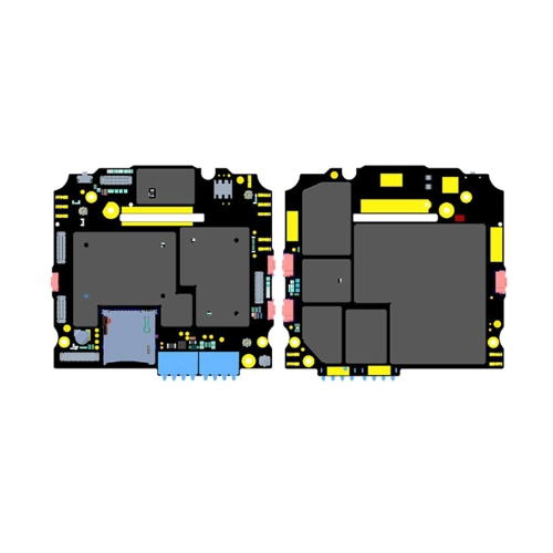
The project started with a detailed review of the MT6833 platform reference design, followed by adjustments based on the handheld PDA’s mechanical structure and industrial use case. Key modules — including the 5G RF section, LPDDR4X memory, power management, scanning interfaces, and battery system — were mapped early to define clear zoning and signal priorities. Special attention was given to PCB outline, connector positioning, and component height limits to match the IP68 enclosure design. These constraints were fixed early to avoid structural changes during later PCB revisions.
High-Speed PCB Layout & DFM Optimization
During layout, 5G RF and high-speed signal routing were handled first, with controlled impedance traces, short return paths, and dedicated ground references. Power paths for the 5G modem and scanning modules were widened and reinforced to handle peak current, while sensitive RF and memory areas were isolated from switching noise. DFM checks were conducted in parallel with layout work, covering stack-up selection, via structures, pad design, and solder mask openings. This allowed potential manufacturing issues to be corrected before the first prototype build.

PCBA, Assembly & Production Validation
After design freeze, pilot PCBA builds were used to validate assembly stability and functional performance. Power-up behavior, 5G connectivity, scanning accuracy, and positioning performance were tested under real operating conditions. Battery hot-swap behavior and connector reliability were also verified to ensure suitability for daily industrial use. Based on these results, the PCB and assembly process were confirmed for volume production, enabling the customer to move directly into mass manufacturing without additional rework cycles.
How We Control Quality in 5G Handheld PDA PCB Projects
Quality risks in a 5G handheld PDA PCB are concentrated in RF consistency, power stability, assembly yield, and long-term reliability. Our quality control is structured around these four areas.
Design Quality Control
RF impedance targets and stack-up parameters were fixed before layout release.
Power and ground strategies were verified against peak 5G transmission current.
Component selection was locked to avoid performance deviation during production.
PCB Fabrication Control
High-frequency laminate parameters and copper thickness were specified for RF stability.
Impedance control and layer alignment were verified on incoming PCB panels.
Functional & Reliability Verification
Power-up behavior, 5G connectivity, and scanning performance were tested under load.
Assembly consistency and connector reliability were verified across production units.

Discuss Your 5G PCB Project
One-stop PCB design & PCBA manufacturing for industrial devices