

In PCB manufacturing, your Gerber files are the blueprint of your circuit board — the one set of documents your manufacturer relies on to create a precise, error-free PCB. A single missing layer, incorrect format, or mismatched drill file can lead to costly rework, production delays, or even unusable boards.
This article will guide you through 9 critical checks you should perform before sending your Gerber files to your PCB manufacturer. By following this checklist, you’ll prevent errors, improve yield, and ensure your design is built exactly as intended.
Before sending your Gerber files to a manufacturer, verify these nine key points: correct RS-274X file format, complete copper and solder layers, accurate silkscreen labeling, aligned drill files, precise board outline, detailed via data, clear surface finish instructions, and correct panelization layout. Always confirm your manufacturer’s DFM review before production.
Let’s walk through each checkpoint in detail — from file format verification to design-for-manufacturing (DFM) preparation — so you can ship your Gerber files with confidence.

1. Check Gerber File Format (RS-274X Compliance)
There are three primary Gerber file formats:
- Gerber X2: The latest standard, which enriches data by embedding layer attributes and stack-up information directly within the files.
- Extended Gerber (RS-274X): The current industry-wide standard, which superseded the older format.
- Standard Gerber (RS-274D): The legacy format that has been obsolete for years and was fully replaced by RS-274X.
Before anything else, confirm that your Gerber files are exported in the RS-274X format. This is the industry-standard format accepted by nearly all PCB manufacturers.

Why It Matters?
Older formats like RS-274D lack embedded aperture data, meaning your manufacturer might not know the exact line widths or pad shapes to use. This can lead to misinterpreted copper layers or incorrect feature sizes.
What to Do?
- Use your PCB design software (Altium, KiCad, Eagle, etc.) to export in RS-274X.
- Double-check that each layer is properly named — e.g.,
TopCopper.gbr,BottomCopper.gbr,TopMask.gbr. - Include a readme.txt file listing every layer’s function.
- Compress all files into one
.zipbefore uploading to your manufacturer’s portal.
Common Mistakes
- Missing aperture definitions in RS-274D format.
- Forgetting mechanical layers or outline layers.
- Sending Gerber and drill files separately without a clear naming convention.
Tip: Many manufacturers provide free Gerber viewers (like HQDFM or Gerbv) to preview files exactly as they’ll be fabricated.
2. Verify Copper Layers (Top and Bottom)
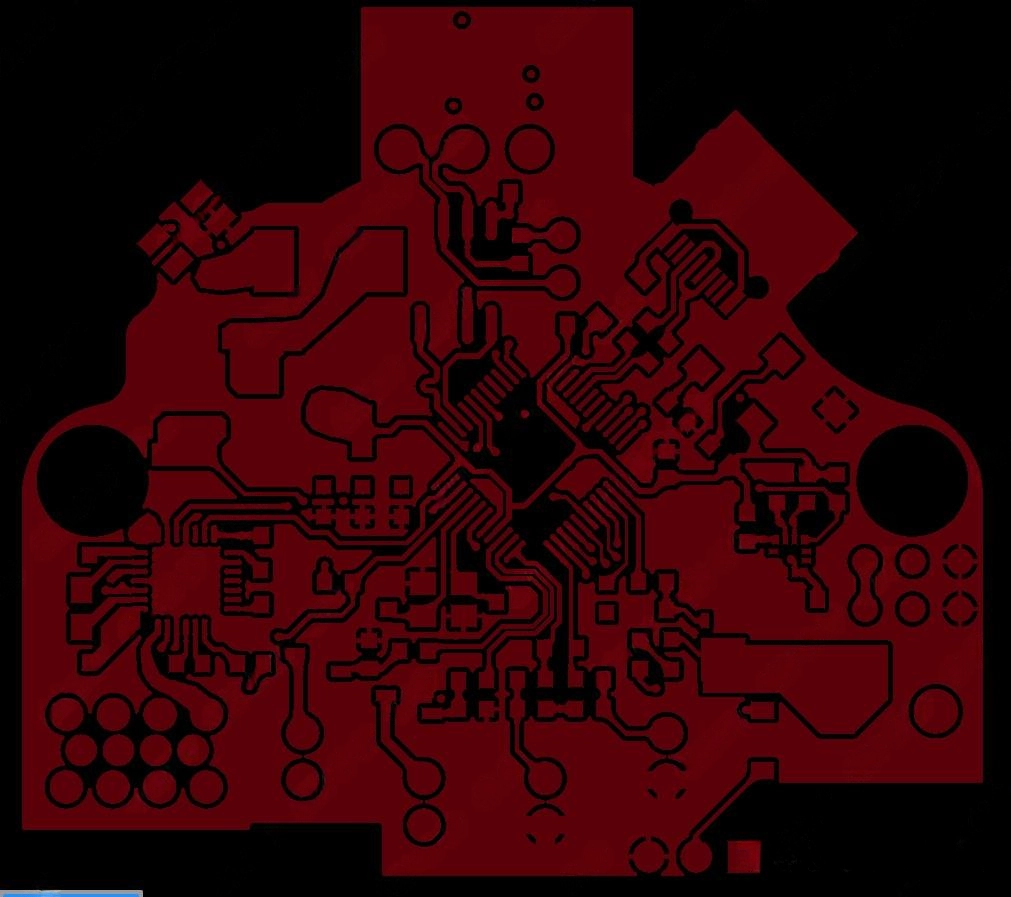
Your copper layers define the electrical backbone of your PCB — every signal, power trace, and ground plane. Any misalignment or missing layer here can cause total board failure.
How to Inspect?
- Open your files in a Gerber viewer and verify that the top and bottom copper layers are present.
- Check that trace widths, clearances, and via sizes meet your manufacturer’s minimum design rules.
- Ensure layer polarity (positive vs. negative) matches your design intention.
- Confirm all copper pours and planes are filled correctly.
Watch for These Red Flags
- Misaligned vias between layers.
- Isolated copper islands (not connected to ground or signal nets).
- Overlapping traces that could be shortened under the solder mask.
Why It’s Important?
Accurate copper data ensures clean etching and consistent impedance during fabrication. Even small deviations can alter circuit behavior or cause signal integrity issues in high-speed designs.
3. Confirm Solder Mask and Paste Layers
The solder mask (often green, but also red, blue, or black) protects your PCB’s copper from oxidation and solder bridges. The paste layer defines where solder paste will be applied for SMD assembly.

What to Check?
- Make sure your Top and Bottom Solder Mask layers are included.
- Verify openings exist only where soldering occurs — pads, vias, and test points.
- Check that the solder mask clearance (the gap between mask and pad) meets the manufacturer’s tolerance (typically 2–5 mils).
- Confirm paste layers align perfectly with the SMD pads.
Common Issues
- Missing solder mask layers lead to full copper exposure.
- Incorrect clearances can cause solder bridging or poor wetting.
- Paste misalignment results in uneven solder distribution and assembly defects.
Pro Tip
Use your PCB software’s solder mask preview mode or a Gerber viewer to visualize exactly which areas will be exposed or covered. Tools like Altium Designer’s 3D viewer help you simulate real production visuals.
4. Inspect the Silkscreen Layer
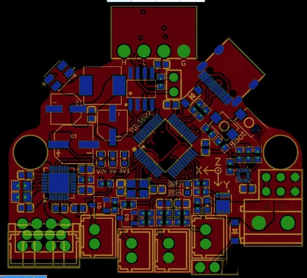
The silkscreen layer is often overlooked, but it plays a vital role during PCB assembly and maintenance. It provides visual information such as component reference designators, polarity indicators, and logos.
Why does it matter?
A clean and accurate silkscreen helps assembly technicians identify components quickly. Misplaced or overlapping silkscreen text can cause confusion and increase the risk of assembly errors.
What to check?
- Make sure all component reference labels are placed on the correct side of the board.
- Ensure the text size is readable and not too small for your manufacturer’s printing process (usually at least 1 mm in height).
- Keep silkscreen markings clear of solder pads to prevent ink contamination during reflow soldering.
- Check for mirrored or flipped text, especially when you have components on both sides of the board.
Common issues
- Silkscreen printed on exposed copper, causing poor adhesion.
- Misaligned component labels that don’t match the actual layout.
- Overlapping text makes the board look messy or unreadable.
A clean, properly aligned silkscreen improves both the appearance and serviceability of your PCB.
5. Review NC Drill Files and Hole Data
Drill files define every hole in your PCB—plated through-holes, vias, and non-plated mounting holes. If these are not accurate, you may face serious alignment problems during fabrication.


How to review?
- Check that all drill files are included, usually with the extensions
.drlor.txt. - Verify that hole sizes correspond to the correct net or component.
- Ensure plated and non-plated holes are clearly marked as such.
- Compare the drill data against your copper layers to confirm proper pad alignment.
Why is this step critical?
Incorrect or missing drill information can result in:
- Holes that are too small for component leads.
- Misaligned vias that do not connect between layers.
- Manufacturing delays, as the factory must request clarification.
Most PCB manufacturers offer automated DFM tools (Design for Manufacturability) that highlight drill-to-copper spacing or missing hole definitions. Always run these checks before submission.
6. Check Board Outline and Dimensions
The board outline defines the exact size and shape of your PCB. It ensures that your board fits perfectly into its enclosure or mechanical assembly.

What to verify?
- Confirm that the outline layer is included and visible in your Gerber set.
- Measure the overall dimensions and compare them to your design specifications.
- Make sure the outline doesn’t overlap with any traces or components.
- If there are cutouts, slots, or irregular shapes, define them clearly using mechanical layers.
Practical tips
- Label the outline layer clearly as “Board Outline” or “Mechanical 1” to prevent confusion.
- Avoid redundant outlines on multiple layers.
- For panelized designs, ensure that each sub-board is separated by routing paths or v-cuts as specified by your manufacturer.
A precise outline helps manufacturers avoid milling errors and guarantees that your PCB matches the mechanical enclosure perfectly.
7. Validate Hidden and Buried Via Details
Modern multilayer PCBs often include blind or buried vias to save space and improve signal integrity. However, incomplete via information is one of the most common reasons for fabrication delays.
What to include?
- Provide a complete layer stack-up document that specifies which layers each via connects.
- Clearly label blind, buried, and through vias in your drill files or separate them into different files.
- Verify that the manufacturer supports the via structure you designed, as some low-cost fabs may not offer microvia or HDI capabilities.
- Confirm that via diameters meet the minimum fabrication limits (typically 0.15 mm for microvias).
Why is it important?
Without accurate via information, manufacturers can’t guarantee electrical connectivity between layers. This could result in an open circuit, incorrect impedance, or failure during electrical testing.
Always review the final via summary in your CAM preview before submission.
8. Confirm Surface Finish and Coating Information
The surface finish is a thin protective layer applied to exposed copper areas to prevent oxidation and ensure reliable soldering. It directly affects solderability, component lifespan, and overall PCB quality.
Common surface finishes
- HASL (Hot Air Solder Leveling): A cost-effective option, suitable for most general-purpose boards.
- ENIG (Electroless Nickel Immersion Gold): Provides a flat surface ideal for fine-pitch components and offers excellent corrosion resistance.
- OSP (Organic Solderability Preservative): A lead-free, environmentally friendly coating used in high-volume production.
- Immersion Silver or Tin: Provides good conductivity and surface flatness but requires careful handling to avoid tarnishing.
What to check before submission?
- Confirm that your chosen finish type is clearly specified in your fabrication notes or Gerber job file.
- If your design includes high-frequency or RF circuits, ensure the finish is compatible with signal performance requirements.
- Verify that no copper areas are unintentionally exposed without coating.
- Discuss with your manufacturer if a specific coating thickness or finish is required for your assembly process.
Why does it matter?
Incorrect or missing surface finish information can cause oxidation, poor solder adhesion, or premature component failure. By defining this clearly, you ensure consistent soldering results and long-term board reliability.
9. Verify Panelization and Multi-board Layout
Panelization refers to grouping multiple PCB units into a single production panel for efficient manufacturing. If your design includes several small boards, panelization helps reduce cost and handling time.

Steps to verify
- Check that your panel drawing or outline is included and matches the manufacturer’s preferred format.
- Ensure that v-cut lines or breakaway tabs are clearly defined and do not interfere with components or traces.
- Confirm that fiducial marks and tooling holes are present on the panel for accurate alignment during assembly.
- Review the spacing between boards—usually a gap of 2 to 3 mm is recommended.
Additional considerations
If your boards are of irregular shapes, discuss custom panelization options with your fabricator. Some manufacturers may prefer to perform panelization themselves to ensure compatibility with their machinery. Providing clear panel drawings helps avoid communication errors and improves manufacturing efficiency.
Additional Suggestions Before Sending Gerber Files
Even after completing the nine-point checklist, it’s smart to take a few final steps before submitting your files:
- Request a DFM (Design for Manufacturability) review.
Many PCB manufacturers provide free or automated DFM reports to catch potential issues, such as trace width violations or missing layers. - Include supporting documents.
Along with your Gerber files, provide the bill of materials (BOM), pick-and-place data, and assembly drawings. These help the manufacturer prepare for both fabrication and assembly. - Double-check your file names and formats.
Consistent naming (for example, “TopCopper.gbr”, “BottomMask.gbr”) prevents mix-ups and speeds up processing. - Communicate with your manufacturer.
If you have special requirements—such as impedance control or non-standard materials—discuss them early. Clear communication minimizes production delays.
FAQs
How to verify Gerber files?
You can use online or offline Gerber viewers, such as HQDFM or Gerbv, to preview your files. These tools enable you to verify that every layer, drill hole, and outline is displayed correctly before manufacturing.
What does a Gerber file contain?
A complete Gerber file set includes data for copper layers, solder mask, silkscreen, drill holes, and the board outline. Each layer is stored separately and guides the manufacturer through every step of the fabrication process.
How do Gerber files ensure manufacturing accuracy?
Gerber files act as digital blueprints. They provide exact coordinates for copper patterns, masks, and drilling operations. This precision ensures that the final board matches the original design and functions as intended.
How can I view Gerber files for free?
There are several free tools available, including HQDFM, ViewMate, and Gerbv. Most allow you to load individual layers, toggle visibility, and align copper and drill data for detailed inspection. It is highly recommended to verify Gerber files using multiple viewers before sending them to the PCB manufacturer. This practice helps identify potential interpretation discrepancies caused by software incompatibilities, ensuring the files are rendered as intended.
Summary
Preparing your Gerber files properly is the key to achieving a smooth, error-free manufacturing process. By following this nine-point checklist—covering everything from file format and copper layers to coating and panelization—you’ll minimize costly revisions, reduce lead time, and ensure that your PCB performs exactly as designed.
If you’re ready to move from design to production, consider partnering with a reliable PCB manufacturer that offers free DFM checks and expert file verification. A few minutes of review today can save you days of rework tomorrow.

