PCB Reverse Engineering Services | Rebuild Schematics & Gerbers
– Recover, Redesign, and Rebuild with Professional Skill
- 48H Fast PCB Delivery
- Gerber Files and Full Test Reports
- Safe and Fast PCB Repair
– Recover, Redesign, and Rebuild with Professional Skill
– Recover, Redesign, and Rebuild with Professional Skill
Unlike basic duplication services, our reverse engineering process is rooted in engineering discipline, manufacturing knowledge, and component-level understanding.
Here’s how we do it — step by step:

Analyzing your PCB sample in detail. This includes counting layers, identifying the board stack-up, measuring dimensions, and capturing component layout using high-resolution imaging and optional X-ray scanning for inner layers.
Rebuild the schematic based on board connectivity and net tracing. This ensures functional accuracy and logical clarity — ideal for troubleshooting, redesign, or further development.
Redraw the PCB layout and regenerate full Gerber files, including copper layers, silkscreen, solder mask, and drill layers. We support popular CAD formats like Altium, Allegro, and OrCAD.
All components are identified, labeled, and matched with standard or equivalent parts. We deliver a complete Bill of Materials (BOM), including part numbers, specifications, and sourcing suggestions — especially helpful if original parts are obsolete.
Perform functional testing on the reverse-engineered board to ensure performance. We also offer layout optimization for better signal integrity, smaller size, or manufacturing cost reduction.
Once complete, we deliver a full documentation package: Gerbers, schematics, BOM, 3D files (if required), and fabrication-ready files — compatible with standard manufacturing processes. You can also proceed directly to prototyping or mass production with us.
Whether you have a bare PCB or a fully assembled board, our team follows a proven step-by-step process to recover your design, reproduce your board, and prepare it for manufacturing or redesign.
What you provide:
Basic product background: what the board is for, what functions it performs
Photos or measurements (if shipping is not immediately possible)
What we do:
Review the complexity of the board (layers, components, routing density)
Determine whether we need partial or full reverse engineering
Estimate lead time and cost
Sign NDA if required
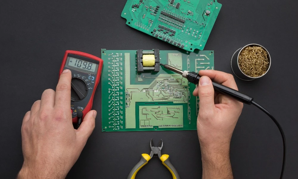
Tools used:
High-resolution photography (top & bottom layers)
Microscopy for fine-pitch components and inner vias
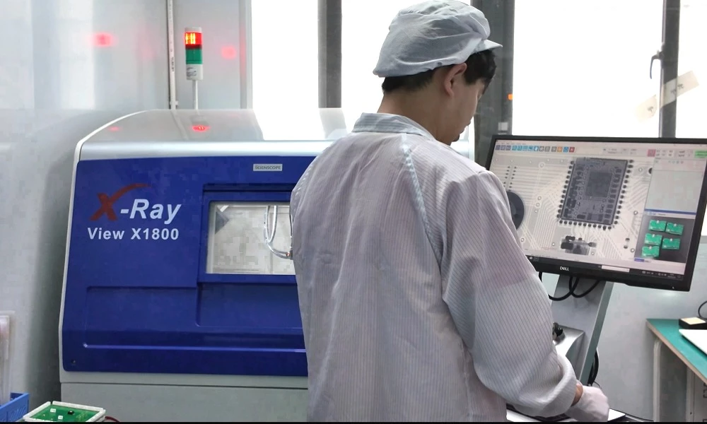
X-ray scanning for internal layer analysis and buried traces
What we extract:
Layer count, via types (e.g., blind/buried), and stack-up
Trace widths, spacing, and via diameters
Component layout, part identifiers, and solder pad shapes
What we do:
Reverse-trace nets based on copper paths and layer interconnects
Map and reconstruct electrical connections in schematic software (e.g., Altium, OrCAD)
Identify component function: resistors, ICs, power supply, I/O interfaces
Cross-reference parts using markings, datasheets, or equivalents if unidentifiable
Challenges handled:
Missing or sanded-off part markings
Multi-pin chips without public datasheets
Multi-layer routing with shared ground/power planes

What we do:
Recreate all PCB layers in CAD, including routing, silkscreen, and mechanical outlines
Apply correct via types, trace widths, and pad shapes
Align with reconstructed schematic to ensure electrical correctness
Build stack-up with correct layer order, impedance zones, and copper weight estimation
Design software used:
Altium Designer, KiCad, OrCAD, or other as per your manufacturing preference

Deliverables include:
Gerber files for each layer (Top/Bottom, Inner, Drill, Mask, Silkscreen, Outline)
Bill of Materials (BOM) in Excel or CSV format
Pick-and-Place / Centroid file for SMT assembly
Schematic source file + PCB layout project files (if requested)
Optionally provided:
3D rendering of board layout
PDF schematic for easier understanding and documentation

Why choose this:
Many clients use reverse engineering not just to recover files, but to rebuild and verify functionality.
What we offer:
Prototype manufacturing based on reversed files
Component sourcing and SMT assembly
Functional testing (basic continuity / power-on / interface behavior)
Engineering support for iterative redesign or enhancements

Before: The original PCB—a broken and complex board without schematics.
After: The replicated PCB—a perfect, functional copy.
This is more than just copying a board. We deconstruct the design, analyze every layer, and create complete documentation for future production.
Need to bring your product back to life? Let's talk about your project.


Choosing the right partner for PCB reverse engineering is critical.
Here’s why engineers, manufacturers, and industry leaders trust us:
Get complete PCB deliverables in as little as 48 hours, minimizing downtime and accelerating your project.
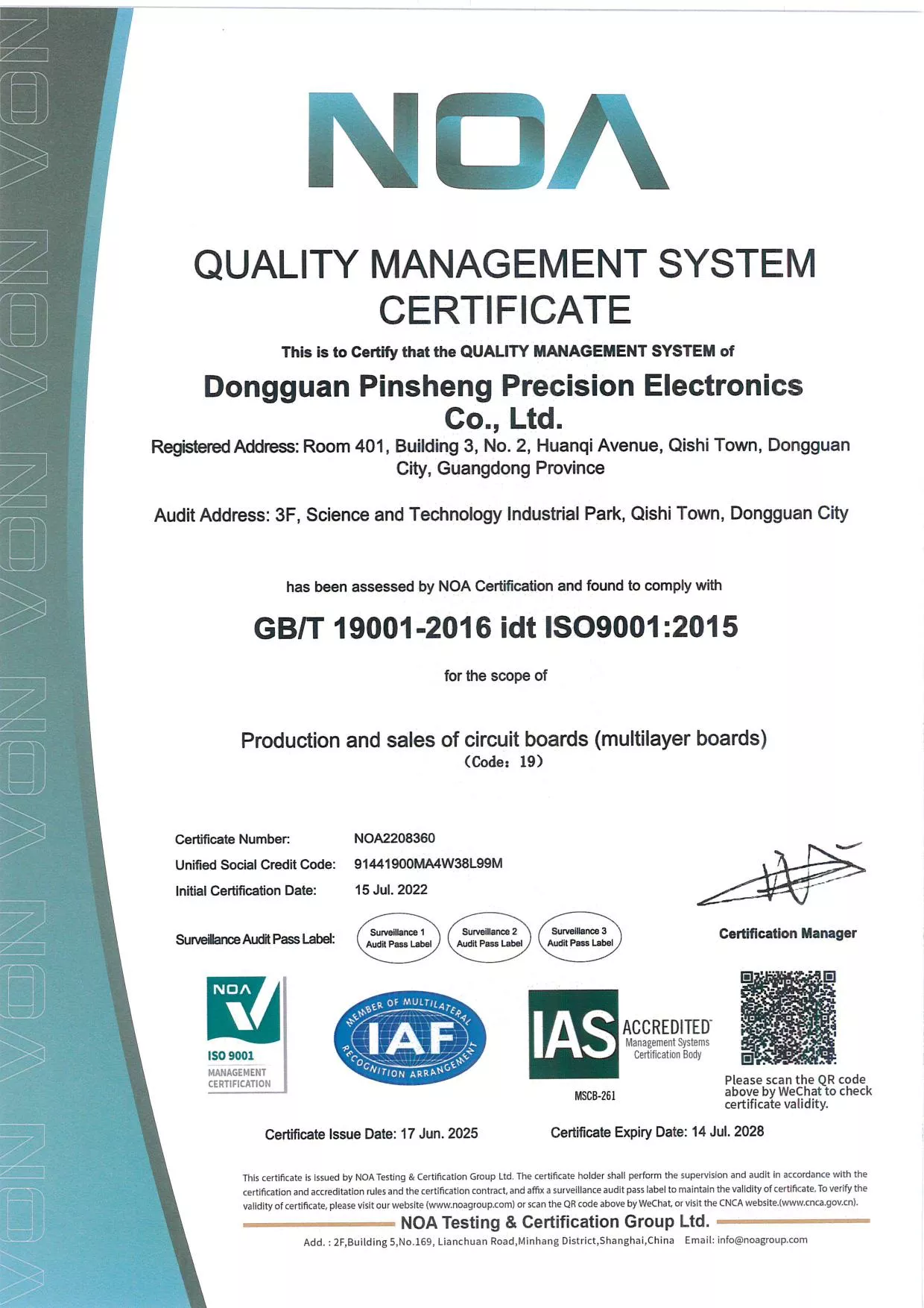
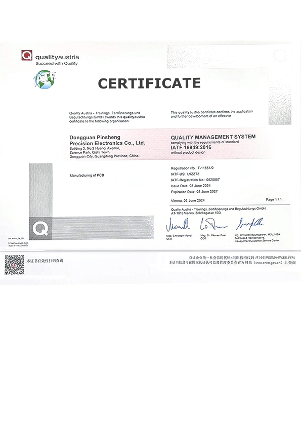
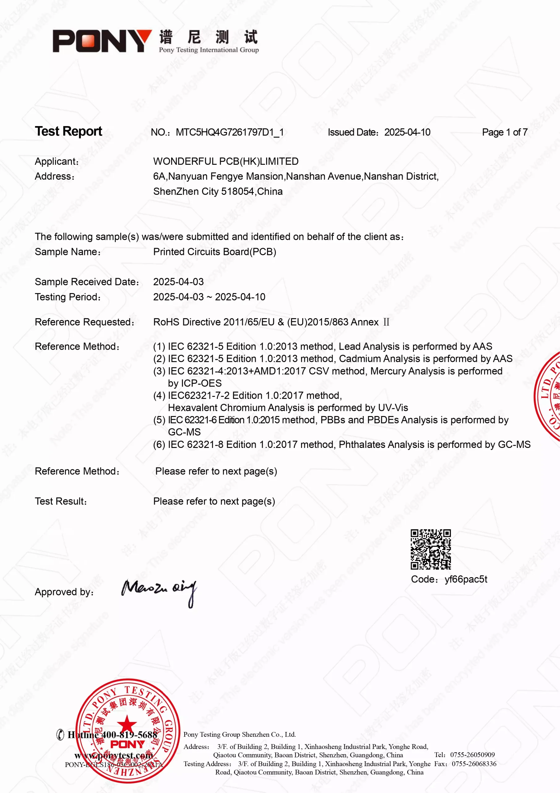
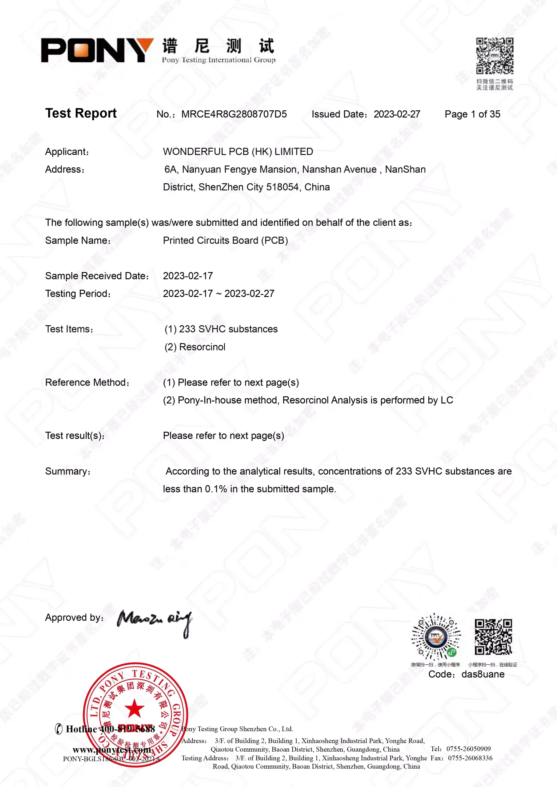
We meet international standards to ensure your projects are safe, stable, and ready for any industry.




Our PCB Reverse Engineering Services are widely used across multiple industries and scenarios:
You need to rebuild the board, but have no access to the original design files. We recreate schematics, Gerbers, and BOM from your physical sample.
You only have a handmade or early prototype. We convert it into a standardized, production-ready PCB
Your product is affected by outdated components. We can help redesign or suggest replacements during the reverse engineering process.
You want to study a competing product or evaluate performance. We helpyou reverse engineer it safely and professionally (within legal and ethicalboundaries).
Your previous manufacturer is no longer available. We help you regain fullcontrol of your product and documentation.
You want to reduce manufacturing costs, improve reliability, or adapt theboard to new environments. We reverse engineer and improve the originaldesign to fit your new needs.
PCB Reverse Engineering is a critical service across a vast spectrum of industries where electronics are essential. Its applications range from maintaining legacy systems to facilitating innovation and competitive analysis.
This is one of the largest and most mature markets for PCB Reverse Engineering. The lifecycle of industrial machinery often exceeds 20 years, while electronic components become obsolete much faster, making RE essential for continuous operation.
PLC (Programmable Logic Controller) Modules: Repairing or cloning obsolete and discontinued PLC modules.
CNC (Computer Numerical Control) Systems: Replacing or upgrading damaged control cards for expensive CNC machine tools.
Robotics Controllers: Maintaining industrial robots, especially for end-of-life models (drive and control boards).
Sensors & I/O Modules: Replicating proprietary signal acquisition and processing modules.
Motor Drives & Inverters: Repairing or replicating specialized drive boards for specific functionalities.
Medical devices are high-value assets with stringent certification requirements. Reverse Engineering is vital for ensuring their operational continuity and reducing maintenance costs, with an extreme emphasis on reliability, safety, and compliance.
Medical Imaging Systems: Repair and replacement of internal boards for CT, MRI, and ultrasound machines.
Patient Monitoring Systems: Providing replacement boards for various models of patient monitors.
Life Support Systems: Core control boards for ventilators, infusion pumps, and defibrillators.
Laboratory Equipment: Internal electronic modules for blood analyzers, DNA sequencers, and other lab instruments.
Modern vehicles contain over a hundred ECUs (Electronic Control Units). The aftermarket, repair, and classic car restoration sectors generate massive demand for reverse engineering.
Engine Management Systems (EMS) / ECUs: Used for repair, performance tuning, or manufacturing replacement ECUs for classic cars.
Body Control Modules (BCM): Repair and replacement of modules for windows, seats, and lighting controls.
Instrument Clusters: Repairing or customizing vehicle dashboards.
Infotainment Systems: Providing repair solutions for head units and audio systems.
EV Powertrain Systems: Research, repair, and learning for BMS (Battery Management Systems), VCU (Vehicle Control Units), and MCU (Motor Control Units).
This sector has extreme requirements for reliability, safety, and long-lifecycle support. Many specialized systems lack off-the-shelf replacement parts.
Avionics: Board-level repair and spare part manufacturing for flight instruments, navigation, and communication systems.
Ground Support Equipment (GSE): Maintenance for testing and support equipment used at airports and launch sites.
Radar & Communication Systems: Maintenance and domestic replacement of boards for military/civilian radar and radio systems.
Satellite & Spacecraft Components: Research and imitation of certain non-core modules.
This field focuses more on learning, competitive analysis, and rapid iteration, alongside a significant repair market.
Smartphones & Tablets: Used for repair, accessory manufacturing, and design research.
Drones (UAVs): Researching core boards (flight controllers, video transmission) for developing compatible products or upgrades.
Smart Home Devices: Research boards for high-end smart speakers, routers, and security cameras.
Gaming Consoles: Repair and aftermarket parts for legacy models of PlayStation, Xbox, etc.
High-End Audio Equipment: Repair and replication of Hi-Fi amplifiers, DACs, and mixing consoles.
Network infrastructure demands 24/7 uptime, making the rapid replacement of faulty boards a critical need.
Network Switches & Routers: Board repair and spare parts for enterprise and carrier-grade equipment.
Base Station Equipment: Maintenance for radio units and baseband units in 2G/3G/4G base stations.
Optical Transmission Equipment: Board-level repair for optical modules and transceivers.
Data Center-specific Hardware: Research and replacement for accelerator cards and storage controller cards.

Built to Manufacture. Built to Deliver.
IWDF Solutions’ Reverse Engineering Center is more than a workshop—it’s the foundation of precision and trust.
With 3,000㎡ dedicated facilities, over 500 skilled engineers and technicians, and 200+ sets of advanced analysis and manufacturing equipment, we handle the entire PCB reverse engineering lifecycle in-house—from circuit board teardown and schematic recovery to Gerber reconstruction, BOM extraction, and prototype reproduction.
Our capabilities cover high-resolution component inspection, CNC micro-drilling, precision routing, automated solder mask application, and comprehensive electrical testing. Every step is executed under strict NDA protection and rigorous quality protocols, ensuring that your intellectual property remains safe while your project is completed with the highest accuracy.
Strict Quality Control at Every Stage
We follow a rigorous quality management system to ensure every board meets your standards — from first prototype to full production.