


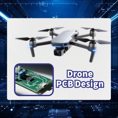
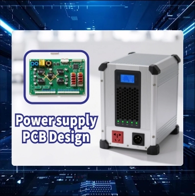
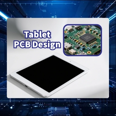

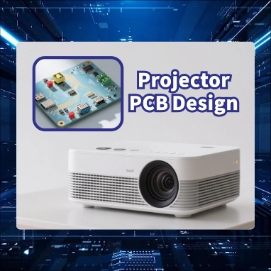
Professional PCB Design Services Tailored to Your Project
From concept to prototype to mass production — Fast, Reliable, and Fully Certified
- Accelerate Time-to-Market
- Reduce Costly Rework
- One-Stop Accountability
Stop losing weeks to outsourced teams, unclear communication, and failed prototypes.
We design and manufacture in-house — fast, reliable, and cost-effective.
From concept to prototype to mass production — Fast, Reliable, and Fully Certified
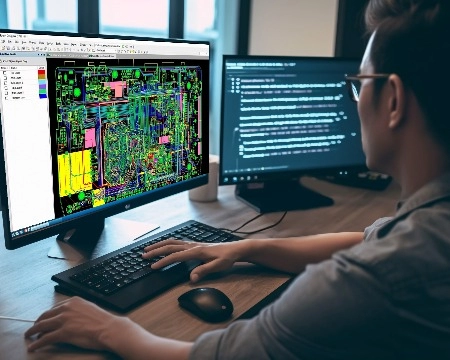
From single-layer pcb to complex multilayer, rigid-flex, heavy copper, HDI, and high-speed boards — IWDF Solutions delivers complete PCB design services. Our engineers can start from your concept or refine your existing design, create fully functional prototypes, integrate embedded software, run thorough performance testing, and provide complete production-ready documentation.
Service Area
Description
Complex applications—like 5G modules, power electronics, or wearable devices—demand more than just basic layout skills. We specialize in high-speed, high-frequency, heavy copper, and multilayer PCB design, ensuring your boards meet performance, reliability, and manufacturability goals from the start.
Ensures signal integrity in DDR, USB 3.0, PCIe, and high-speed buses.
Controlled impedance ±10%, length matching, signal simulation.
Prevents signal loss in RF circuits for IoT, antennas, wireless modules.
Up to 6 GHz support, RF path tuning, antenna matching, low-loss stackup.
Handles high current and thermal dissipation in power electronics.
Up to 6 oz copper, IPC-2221-based design, via stitching for current paths.
Enables compact form factors for advanced electronics (wearables, medical, etc.)
32 layers, blind/buried vias, BGA escape routing, impedance modeling
We begin by deeply understanding your project goals, target application, performance requirements, mechanical constraints, and budget.
Once the concept is clear, we translate functional requirements into an optimized schematic design using professional EDA tools (Altium, OrCAD, KiCad, etc.).
This is where the real engineering finesse comes in — transforming schematics into manufacturable layouts.
Every design goes through internal cross-checks and DFM/DFA/DFT analysis to ensure it’s ready for fabrication and assembly without surprises.
Optional: We run the design past your contract manufacturer for joint validation.
Once the layout is finalized, we prepare a complete manufacturing documentation package:
After design handoff, we stay involved to ensure smooth production and validation:
Proven Capabilities, Trusted by Global Clients
With 20+ years of industry experience, we’re more than just a PCB service provider — we’re your full-cycle engineering and manufacturing partner.
Fast design cycles mean you can test and launch products weeks earlier — keeping you ahead of competitors.
Layouts are optimized for EMI/EMC compliance, manufacturability, and long-term reliability — reducing failed prototypes and costly rework.
Early cost estimation and risk mapping give you the insights to make informed design decisions. This helps prevent expensive redesigns, delays, and wasted materials later in the process.
Every project comes with complete design documentation — Gerber, BOM, assembly instructions — ensuring smooth handoff to manufacturing and fewer surprises.
With both design and production under one roof, you get a single partner fully responsible for outcomes — no finger-pointing between vendors.
Our PCB design solutions are trusted by companies in:
We are more than just designers – we are your engineering partner.
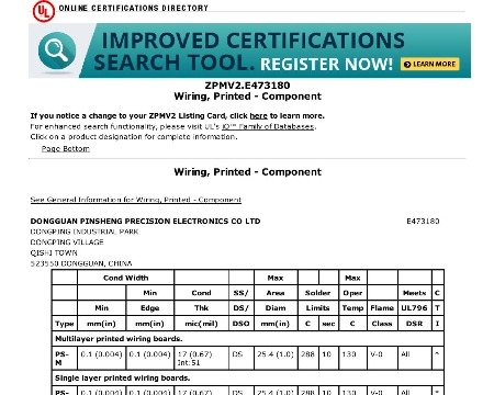
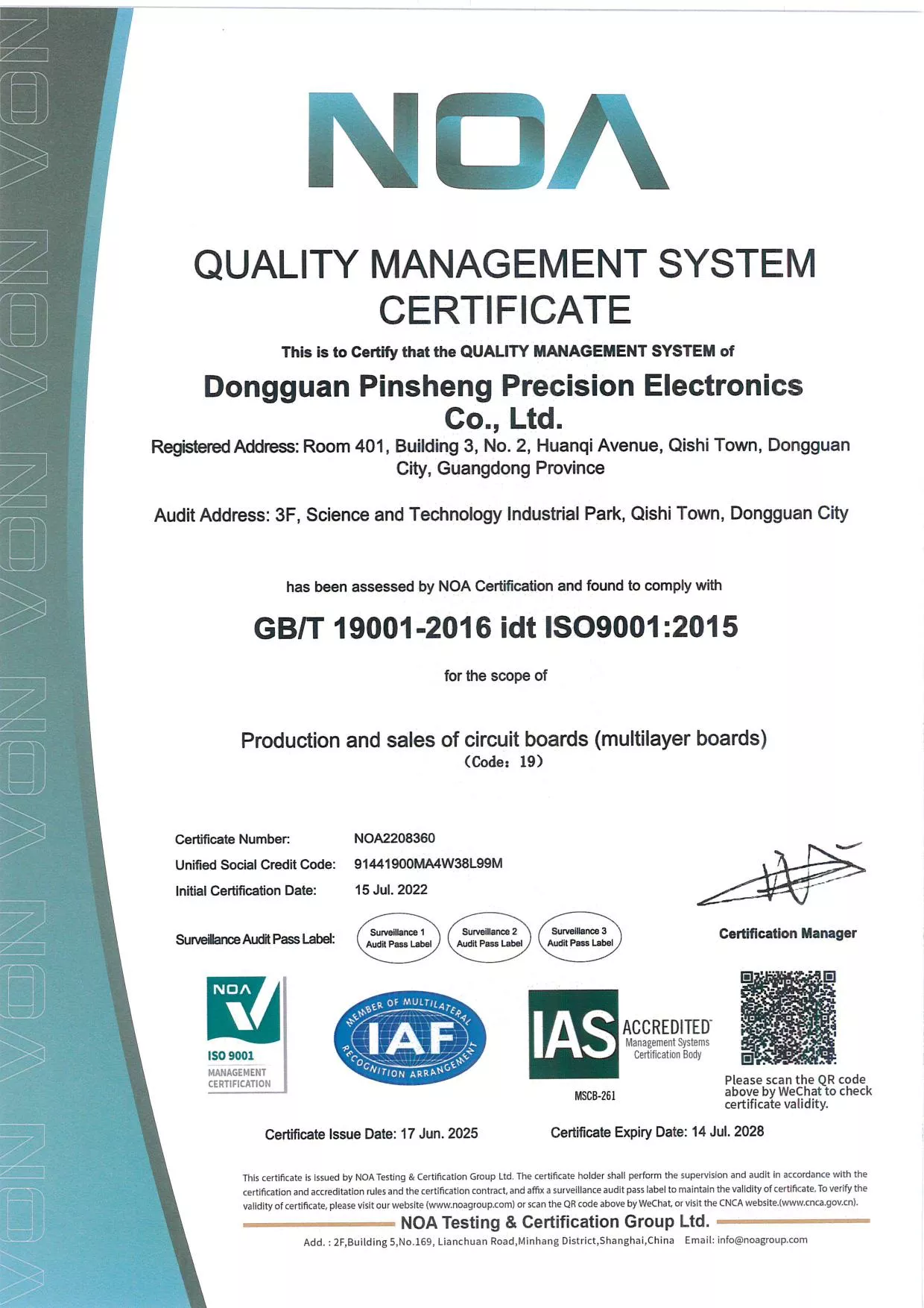
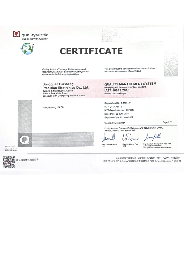
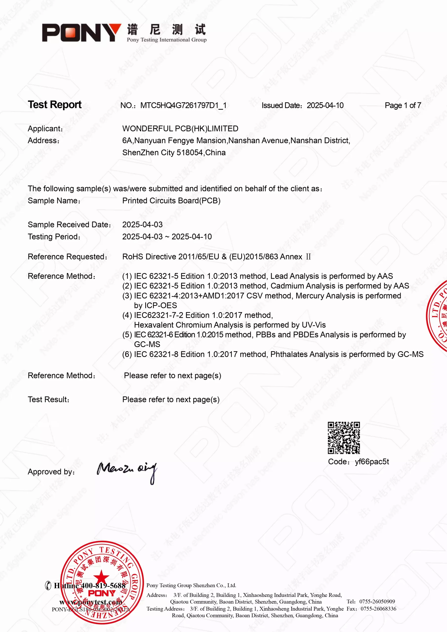
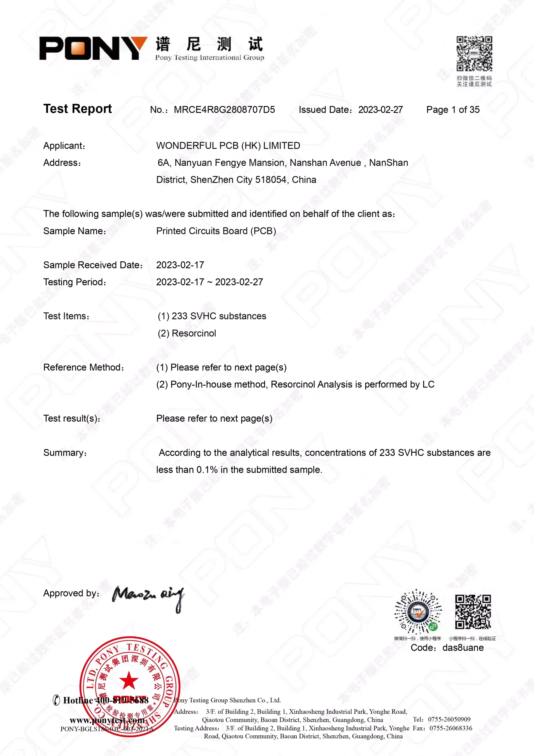
We meet international standards to ensure your projects are safe, stable, and ready for any industry.


Built to Manufacture. Built to Deliver.
IWDF Solutions’ PCB facility is more than a factory — it’s where reliable boards are born.
With 3,000㎡ of dedicated production space, 500+ skilled staff, and over 200 sets of advanced design, manufacturing, and inspection equipment, we manage the entire PCB lifecycle in-house — from schematic capture and layout engineering to prototyping, mass production, and final testing.
From high-speed multilayer routing and impedance-controlled stack-ups to CNC drilling, automated solder mask printing, and 100% electrical testing, every step is executed under strict quality protocols. By integrating design and manufacturing under one roof, we reduce rework, accelerate turnaround, and ensure your boards meet both performance and compliance standards the first time.
Strict Quality Control at Every Stage
We follow a rigorous quality management system to ensure every board meets your standards — from first prototype to full production.
To provide an accurate quote, we typically require:
-Schematic diagrams or design files
-Bill of Materials (BOM)
-Mechanical constraints or enclosure details
-Specific design requirements (e.g., impedance control, layer count)
-Target production volume and timeline
We support Altium Designer, CAD, or PADS, Allegro, and Eagle. Deliverables include Gerber, BOM, and Pick & Place files.
Yes, we offer expedited services, with turnaround times based on project complexity. Feel free to contact us to discuss the details.
Turnaround times vary based on project complexity. Simple designs may take a few days, while more complex, multi-layer boards could require several weeks. We provide estimated timelines after reviewing your project requirements.
Absolutely. Every project includes DFM/DFA review to avoid costly manufacturing errors.
Absolutely. Our engineers are experienced in designing high-speed and RF PCB, incorporating best practices for signal integrity, impedance matching, and minimizing electromagnetic interference.
Absolutely. We can assist at any stage of your design process, whether you’re starting from scratch or need support refining an existing schematic.
Yes. We specialize in layout improvements, size reduction, DFM enhancements, and thermal/signal integrity optimization.
We’ve designed PCB for IoT, automotive, consumer electronics, medical, industrial control, and robotics applications.
We offer end-to-end solutions, including prototyping and full-scale production. Our manufacturing facilities are equipped to handle various production volumes with high-quality standards.
Absolutely. We sign NDAs, and our facility complies with strict IP protection protocols.
You can start by contacting us through our website, WhatsApp number, or directly via email. Provide us with your project details, and our team will guide you through the next steps, including quoting and project planning.