

PCB reverse engineering and cloning offer significant business advantages—faster time-to-market, reduced design costs, and the ability to replicate proven functionality across new product lines or manufacturing geographies. Yet countless engineering teams discover that their cloned PCBs fail in production, leading to costly delays, wasted components, and damaged customer relationships. The problem is rarely random; it stems from systematic gaps in the reverse engineering, design transfer, manufacturing execution, or quality validation stages.
This guide addresses why cloned PCBs malfunction and provides actionable diagnostic and remediation pathways. Whether you’re an engineer troubleshooting a failed board, a procurement manager evaluating reverse engineering vendors, or a product leader planning a cloning initiative, understanding these seven failure categories will help you identify root causes quickly, implement targeted fixes, and avoid repeating mistakes in scaled production. We’ll walk you through real diagnostic techniques, executable verification steps, and the importance of end-to-end process control—critical factors that separate high-reliability cloned boards from unreliable knock-offs.
1. Dimensional and Positioning Errors: The Foundation Problem
The Core Issue
Cloned PCBs often fail at the most fundamental level: physical dimensions and mechanical positioning. Misalignment of the outer profile, drilled holes, mounting holes, and silkscreen markings may seem like minor cosmetic issues, but they cascade into functional failures during assembly and deployment. A board that doesn’t fit the target enclosure or connector footprints won’t assemble correctly, regardless of electrical integrity.
Dimensional errors typically originate during the reverse engineering phase. When extracting layout data from an original board—whether through X-ray imaging, mechanical measurement, or layer-by-layer disassembly—small measurement errors, scaling mistakes, or incomplete documentation compound as the design moves into production. A tolerance error of just ±0.1mm across mounting holes can prevent proper alignment in automated pick-and-place equipment or cause loose connectors post-assembly.
Diagnostic Approach
To identify dimensional root causes, compare the original reference board against your cloned output using a systematic methodology:
Physical Overlay and Measurement: Use digital calipers or coordinate measuring machines (CMM) to verify overall board dimensions, corner radii, and critical hole positions on both the original and cloned boards. Document all measurements in a standardized tolerance matrix.
Mechanical Test Fit: Physically insert the cloned PCB into its target connector, enclosure, and mechanical assembly to validate fit. This is the fastest reality check—if the board doesn’t slide smoothly or sits unevenly, dimensional errors are present.
Drill and Hole Comparison: Extract drill files (Excellon format) from both the original gerber dataset and your cloned design files. Overlay these files in PCB design software (such as KiCad, Altium, or Eagle) to identify discrepancies in hole diameter, position, and quantity. Mismatched hole counts or positions often reveal incomplete layer extraction.
Silkscreen and Reference Overlay: Compare silkscreen and solder mask layer images. Reference designators (R1, C2, etc.), polarity indicators, and assembly notes that are misaligned or missing will confuse assembly technicians and increase error rates.
Remediation Steps
Once dimensional errors are confirmed, the fix requires discipline and documentation rigor:
- Re-extract Layout Data: Return to the original imaging and measurement step. If using X-ray or automated extraction tools, validate output against manual verification on select critical features (at least 10–15 critical dimensions). Cross-check against assembly drawings if available.
- Tolerance Tightening: Establish and document tolerance bands for each dimension class. Mechanical holes should typically hold ±0.05–0.10mm tolerances; edge profiles should be ±0.2mm. Silkscreen positioning should be ±0.25mm to ±0.5mm, depending on feature size.
- Design Review Gate: Require formal sign-off on dimensional data before releasing to manufacturing. This includes a mechanical engineer or technical lead comparing the cloned design Gerber to the original reference in overlay view.
- Manufacturing Feedback Loop: After the first production run of a cloned board, capture as-built measurements from production (from drilling, routing, and inspection steps) and feed them back into the design database for continuous refinement.

2. Copper Foil and Conduction Defects: Shorts and Opens
The Core Issue
Electrical failures in cloned PCBs frequently stem from trace routing and via placement errors that create unintended shorts (conductors touching that shouldn’t) or opens (broken traces or missing connections). These defects may escape initial visual inspection but trigger failures during power-on, thermal stress, or signal integrity testing. Copper defects also include oversized or undersized pads that lead to poor solder joint formation or tombstoning during reflow.
The roots of these failures often trace to incomplete or inaccurate reverse engineering of inner layers in multilayer boards. When extracting copper patterns from internal layers—a challenging task requiring careful imaging or progressive layer removal—slight errors in trace width, via placement, or plane layer definition can introduce unwanted connections or severed paths.
Diagnostic Approach
To pinpoint conduction defects:
Automated Optical Inspection (AOI) Reports: Request detailed AOI data from your contract manufacturer, focusing on areas flagged for copper bridging, insufficient annular ring (the copper ring around a drilled via), or trace width violations. AOI systems using high-resolution cameras can detect solder bridges and copper anomalies invisible to the naked eye.
In-Circuit Test (ICT) Failure Maps: If available, retrieve ICT test reports that map short or open failures to specific nodes. This instantly identifies which nets are affected and narrows the diagnostic scope.
Microscopic Layer Analysis: For suspected inner-layer shorts, progressively remove copper layers using a PCB layer removal or section kit under a microscope. This destructive but definitive technique reveals exactly where copper bridging occurs and confirms the fault is in the design, not the manufacturing process.
Thermal Stress Assessment: Subjected cloned boards to thermal cycling (e.g., -20°C to +85°C for 10–20 cycles) before electrical testing. Marginal solder joints or stress-induced failures often surface under temperature variation, revealing robustness issues early.
Remediation Steps
Addressing conduction defects requires both design correction and process refinement:
- Trace and Via Re-verification: Using high-resolution imaging (such as X-ray or cross-sectioning), re-examine all inner layers of the original board. If inner-layer detail is unclear, engage a specialized PCB imaging lab or the original manufacturer (if cooperative) for authoritative layer extraction.
- Design Rule Check (DRC) and Spacing Audit: Load your cloned Gerber files into PCB design software and run a full DRC with tight spacing rules (minimum 0.1mm trace-to-trace, proper annular ring sizing). Manually inspect any DRC violations and correct them.
- Copper Pattern Overlay: Overlay your cloned copper layers (inner and outer) against the original reference image, layer by layer. Use transparency or side-by-side comparison views to spot missing traces or unexpected copper additions.
- Manufacturing Process Optimization: Coordinate with your contract manufacturer to optimize masking, etching, and electroplating parameters. Inadequate masking or over-etching can create unintended copper removal; under-plating can cause open circuits in fine-pitch vias.
- Enhanced Testing Protocol: Implement 100% ICT testing on initial production batches, not just sampling. Subsequent production can scale back testing once confidence is established.
3. Interlayer Misalignment: The Multilayer Challenge
The Core Issue
Multilayer PCBs are particularly vulnerable to interlayer registration failures. When copper layers are not precisely aligned during lamination, signal traces on inner layers can shift relative to vias, causing opens or shorts. In high-density designs with fine-pitch traces or densely packed via arrays, even small alignment errors—on the order of ±0.05mm—can break critical connections or create unintended bridges. Misalignment becomes especially problematic in controlled impedance designs where trace position directly affects electrical characteristics.
Interlayer misalignment often originates during reverse engineering of multilayer boards when individual layer patterns are imaged or extracted in isolation and then recomposed without precise positional reference markers. Lamination process drift during manufacturing can compound these errors if the original board design lacked robust alignment features.
Diagnostic Approach
To detect and measure interlayer misalignment:
Via Registration Marks: Examine via arrays and test pads that should be perfectly centered on inner-layer features. Use high-resolution X-ray or cross-sectioning to visualize via position relative to underlying traces. Systematic via misalignment—where vias consistently shift in one direction—indicates design-level misalignment, while random via offset suggests manufacturing drift.
Inner-Layer Imaging and Overlay: Obtain high-resolution scans of each inner layer (through imaging labs or destructive layer-by-layer removal). Import these images into a CAD system and overlay them with registration markers. Measure the positional offset of key features (trace nodes, pad centers, test points) across layers.
Functional Connectivity Testing: Build a test continuity map for your PCB design, identifying all expected connections through vias. Using a curve tracer or continuity probe, verify these paths on both the original and cloned samples. If vias are consistently open or intermittent on the cloned board but functional on the original, alignment is the likely culprit.
Stress Testing Under Load: Thermal and mechanical stress can expose marginal alignment. Apply thermal cycling and vibration testing; if failures spike under stress (especially in high-density via areas), misalignment combined with mechanical stress is the probable cause.
Remediation Steps
Correcting interlayer misalignment requires precision in both design and manufacturing:
- Design Realignment: Re-extract all copper layers from the original board using the most precise imaging or disassembly method available. Establish a master reference layer (typically the component layer) and use it to register all other layers. Ensure each layer’s positional origin is locked to a common datum.
- Lamination Process Specification: Publish tight lamination tolerances for your contract manufacturer, specifying maximum allowable interlayer shift (typically ±0.05mm for fine-pitch designs). Request that the lamination process capability (Cpk) be validated through witness coupons.
- Alignment Feature Integration: In the cloned design, add witness marks or alignment targets (small, isolated test pads or via arrays) positioned at edges or corners. These targets allow the manufacturer to verify alignment post-lamination and serve as early warning for process drift.
- Interlayer Continuity Testing: Implement net connectivity testing on initial production samples, specifically probing via chains (sequential vias connecting across multiple layers). This catches interlayer opens before boards reach functional test.
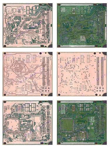
4. Signal Integrity and Impedance Deviation: High-Frequency Failures
The Core Issue
In high-speed and high-frequency PCB designs, trace routing, via placement, and layer stackup directly determine signal behavior. Cloned boards that don’t faithfully reproduce these details will exhibit signal integrity failures—reflections, crosstalk, timing skew, and attenuation—that cause data corruption or functional failure at operating speed. These failures may not appear at low clock frequencies but become severe as data rates increase.
Common impedance-related issues in cloned boards include incorrect trace widths (even small deviations alter characteristic impedance), via stub lengths that introduce reflections, insufficient ground return paths, and improper differential pair spacing or length matching. During reverse engineering, extracting these fine geometric details from the original board is challenging; errors are often made or details overlooked.
Diagnostic Approach
To assess signal integrity in cloned boards:
Impedance Profiling: Use a network analyzer (HP/Agilent 4395A or equivalent) or time-domain reflectometer (TDR) to measure the characteristic impedance of critical traces on both the original and cloned boards. Compare the measured impedance curve against the target specification. Deviations greater than ±10% of the target impedance indicate design discrepancies.
Stackup Verification: Confirm the layer stackup (number of layers, dielectric type, copper weight, spacing) on both boards matches the original specification. Cross-section the cloned board and measure the dielectric thickness between the signal and return planes. Stackup errors directly alter impedance and propagation delay.
High-Frequency Functional Testing: If the design includes test points or accessible nodes, inject a known high-frequency signal (at the target operating frequency or slightly higher) and capture waveforms at input and output using an oscilloscope or logic analyzer. Compare signal quality (amplitude, rise time, ringing) between original and cloned boards. Excessive ringing or attenuation on the cloned board suggests impedance mismatch.
Differential Pair Analysis: For differential signaling (common in high-speed interfaces like LVDS, PCIe, or DDR), measure pair-to-pair spacing, trace width uniformity, and length matching on the cloned board. Use PCB design software to extract these parameters from Gerber files and cross-check against the original reference.
Propagation Delay Measurement: If the design includes matched-length traces (critical for parallel data buses), measure end-to-end propagation delay using a time-domain reflectometer. Delays should match within nanoseconds; large deviations indicate layout changes during cloning.
Remediation Steps
Correcting signal integrity issues requires precision in design and sometimes iterative tuning:
- Detailed Stackup Documentation: Extract and document the complete layer stackup from the original board: material types (FR-4, polyimide, etc.), copper weights, dielectric constants, and spacing. Publish this as a formal layer definition for manufacturing and design reference.
- Trace and Via Re-routing: If trace routing was incomplete or inaccurate during cloning, invest in a full re-trace of critical signal paths. Use impedance-controlled routing modes in PCB design software, specifying target impedance and applying real-time DRC rules during layout.
- Via Placement Refinement: Minimize via stubs on high-speed signals by placing vias on the reverse side if routing permits, or using blind/buried vias to reduce stub length. Route return paths directly underneath signal traces to maintain controlled impedance.
- Length Matching Implementation: For parallel data buses or differential pairs requiring matched propagation delay, apply automated length matching tools in PCB design software. Trace length tolerance should be tighter for higher-speed interfaces (e.g., ±5mm for DDR4 signals).
- Controlled Impedance Testing: On initial production runs, include witness coupons (test traces built alongside the main PCB during manufacturing) and measure their impedance post-production. This validates that the manufacturing process achieves the intended impedance and provides feedback for process tuning.
5. Surface Treatment and Solderability Issues: Assembly Reliability
The Core Issue
Surface finish and solder pad preparation directly impact assembly quality and long-term reliability. Cloned boards that don’t replicate the original surface treatment may exhibit poor solder wetting, tombstoning (components standing on end during reflow), cold solder joints, or accelerated corrosion. These failures manifest as intermittent faults during thermal cycling or accelerated life testing.
Common surface treatment defects in cloned boards include incorrect pad sizing (undersized pads compromise solder joint strength; oversized pads promote solder bridging), incomplete or inconsistent surface coating (HASL—Hot Air Solder Leveling, ENIG—Electroless Nickel Immersion Gold, or OSP—Organic Solder Preservative), and residual flux or contamination from the manufacturing process. During reverse engineering, the original surface finish specification may be assumed or incorrectly identified, leading to production orders with mismatched finishes.
Diagnostic Approach
To diagnose surface treatment and solderability issues:
Pad Size and Clearance Audit: Measure pad dimensions on the original and cloned boards using calipers or a microscope. Cross-check against IPC standards (IPC-2221 for specific applications). Undersized pads should be immediately flagged for redesign.
Surface Finish Identification: Examine the coating appearance under magnification. HASL appears lumpy and variable; ENIG appears smooth and shiny; OSP appears clear or slightly bronze-tinted. If the original is ENIG and your cloned board is HASL, solderability characteristics will differ significantly.
Wettability Testing: Perform wetting balance testing (per ASTM B733) on witness coupons or spare boards, measuring the speed and completeness of solder wetting. Poor wetting (slow wetting or incomplete coverage) indicates surface contamination or improper finish.
Reflow Simulation and Thermal Cycling: Assemble a small batch of cloned boards with test components and subject them to standard reflow profiling plus extended thermal cycling (-40°C to +125°C, 10+ cycles). After thermal stress, cross-section the solder joints under a microscope to assess joint integrity and voids. Compare void percentage and joint morphology to the reflow-tested original boards.
Flux Residue Analysis: If assembly and soldering issues persist, have a sample board analyzed for flux residue through X-ray fluorescence (XRF) or chemical analysis. Excessive or incompatible flux residue indicates cleaning or surface preparation defects.
Remediation Steps
Fixing surface treatment issues requires process specification and manufacturing validation:
- Surface Finish Specification Confirmation: Document the original board’s surface finish specification (HASL, ENIG, OSP, or other) and confirm this specification in all manufacturing orders for cloned boards. Request certificates of compliance from your contract manufacturer, verifying finish type and coating thickness.
- Pad Design Conformity: Cross-check pad sizes in your cloned design against IPC-2221 minimum and preferred ranges for the component types being used. Apply a pad generator tool in your PCB design software to ensure consistency across all pad shapes.
- Manufacturing Process Specification: Publish detailed surface treatment specifications, including: finish type, coating thickness, cleanliness requirements, and pre-soldering handling procedures. Require witness coupons for each production batch.
- Solderability Validation: Include solderability testing (wetting balance or selective solder trials) on initial production runs. If issues arise, adjust cleanliness, flux, or reflow profile in collaboration with your assembly partner.
- Storage and Handling Protocols: Brief your supply chain on proper handling and storage of finished cloned boards (humidity control, inert atmosphere or desiccant packaging) to prevent oxidation and maintain solderability over time.
6. Insufficient Test Coverage: The Hidden Failures
The Core Issue
Test coverage is the final safeguard against shipped failures. Many cloned PCBs appear electrically sound during basic continuity or limited functional testing but fail under real-world conditions—thermal stress, vibration, high-current operation, or edge-case signal sequences. Inadequate test specifications typically result from incomplete reverse engineering of the original design’s test infrastructure or from cost-cutting measures during manufacturing.
Without comprehensive test coverage, defects in other categories (interlayer alignment, impedance deviation, solder joint weakness) slip through to customer deployment, resulting in field failures and warranty costs. The cost of post-production test improvements is dramatically lower than field failure mitigation.
Diagnostic Approach
To assess test coverage gaps:
Test Plan Audit: Obtain the test plan from your contract manufacturer and cross-check it against the original board’s test requirements (if available from documentation or reverse engineering). Common test types include: Automated Optical Inspection (AOI), In-Circuit Test (ICT), functional test, temperature cycling, vibration, and high-potential (hipot) testing.
Failure Mode Analysis: Review field failure data or customer complaints from prior cloned board deployments. Categorize failures by mode (electrical, mechanical, thermal, etc.) and assess whether your test plan would have caught each failure type. If a failure mode slipped through, the corresponding test is missing or insufficient.
Component and Assembly Verification: Confirm that the ICT or functional test is configured to check all critical signal paths, power distribution, and logic nodes. A sparse test (checking only a few nets) will miss many defects; comprehensive tests (coverage >90% of nets) catch most functional issues.
Thermal and Mechanical Stress Testing: For field-deployed boards, simulate actual operating stresses: thermal cycling matching the product’s temperature range (e.g., -10°C to +50°C for consumer electronics, -40°C to +85°C for industrial), vibration per IEC 60068-2-6 (random vibration profile), and moisture absorption per IPC-TM-650 standard practices.
Remediation Steps
Extending test coverage involves specification, process changes, and iterative refinement:
- Comprehensive Test Specification: Define a test plan that covers: 100% AOI (visual inspection), 100% ICT (if test points allow), functional test at nominal and stress conditions (temperature extremes, supply voltage margins), and accelerated life testing (thermal cycling, vibration) on initial production lots.
- In-Circuit Test Point Design: If the original board lacks built-in test points, add non-invasive test nodes (small, isolated pads or via arrays) to critical signal nets during cloning. These points enable ICT access and improve fault detection.
- Functional Test Sequence: Develop a functional test that exercises all major functional blocks: power supplies, clock generation, signal processing, and communication interfaces. Test both nominal conditions and edge cases (minimum/maximum supply voltage, temperature extremes, high data rates).
- Temperature and Stress Testing on Sample: Before full production, conduct thermal cycling and vibration testing on at least 5–10 sample boards from the first manufacturing run. If failures occur, feed results back into design or process improvements.
- Traceability and Root Cause Analysis: When test failures occur, capture detailed failure data (which test failed, at what condition, which component/node was affected). Conduct root cause analysis to determine if the issue is design-level or process-level, informing corrective actions.


7. Bill of Materials and Supply Chain Mismatches: Hidden Incompatibilities
The Core Issue
A cloned PCB design may be perfectly correct, but incorrect or incompatible components will cause functional failures. During reverse engineering, extracting an accurate Bill of Materials (BOM) from the original board requires careful component identification and documentation. Errors—such as wrong package types, incorrect part numbers, substituted alternatives, or sourcing from unreliable vendors—create functional or reliability issues that surface during assembly or operation.
Supply chain mismatches also arise from component obsolescence, vendor differences (chips manufactured by different companies may have subtle parametric differences), or counterfeit parts. In high-volume production, these small differences compound into systematic failures.
Diagnostic Approach
To verify BOM accuracy and supply chain integrity:
Component Cross-Check: Physically identify each component on the original board using package markings, datasheets, and reference design documentation. Verify part numbers, package codes, voltage ratings, and manufacturer names. Cross-reference against your cloned BOM to identify discrepancies.
Parametric Data Validation: For critical components (power supplies, oscillators, high-speed interface chips), verify that key parameters match between original and planned clone: voltage rating, frequency tolerance, slew rate, propagation delay, temperature range. Even minor parametric differences can introduce failures.
Supplier and Sourcing Verification: Confirm that components specified in the cloned BOM are from authorized distributors or original equipment manufacturers (OEMs), not grey-market or counterfeit sources. Request certificates of authenticity for critical components in initial production runs.
Incoming Component Testing: On the first production run, inspect a sample of incoming components for correctness: package appearance, date codes (verify not excessively old), functionality via basic testing (resistance values, capacitance measurements, IC functional tests). This catches component errors before assembly.
Functional Testing with Cloned BOM: Assemble a small batch using the cloned BOM and test for functional performance. If performance differs significantly from the original board (different power consumption, noise characteristics, operating temperatures, or failure rates), component mismatch is likely.
Remediation Steps
Ensuring BOM accuracy and supply chain integrity requires discipline and documentation:
- BOM Documentation and Version Control: Create a comprehensive, versioned BOM document that includes: part number, manufacturer, package type, voltage/power/frequency rating, and approved supplier. Maintain this BOM as the single source of truth for all production orders.
- Component Qualification: For components critical to function or reliability, request datasheets and parametric data from the original manufacturer (not substitutes or grey-market suppliers). Verify that parameters meet or exceed original design specifications.
- Approved Supplier List (ASL): Maintain an approved vendor list for each component type. Require production orders to source only from approved vendors. Periodically audit suppliers for quality and authenticity compliance.
- Counterfeit Detection: Implement counterfeit detection procedures (visual inspection, functional testing, documentation verification) on high-value or mission-critical components. Request traceability from suppliers (batch numbers, manufacturing dates, supply chain documentation).
- Design Flexibility and Alternatives: Document approved alternative parts and packages for common components (e.g., if the original uses a 0805 resistor, qualify a 1206 footprint as an alternative for increased mounting stability). This reduces supply chain risk during component shortages or obsolescence.
- Supply Chain Traceability: Establish a traceability system that links each production batch to its component suppliers and manufacturers. This enables rapid response if counterfeits or quality issues emerge in the supply chain.
Why Choose IWDF Solutions for Cloned PCB Diagnosis and Production
Successfully diagnosing and fixing cloned PCB failures requires expertise spanning reverse engineering, design validation, manufacturing process control, and quality assurance. IWDF Solutions brings two decades of experience in PCB cloning, high-complexity design, and full-scale manufacturing—combined with a commitment to transparency and technical rigor.
Our Diagnostic and Remediation Capabilities
- Design and Reverse Engineering: Our engineering team extracts copper patterns, stackup data, and component layouts from original reference boards using high-resolution X-ray imaging, precision mechanical measurement, and layer-by-layer disassembly. We cross-verify extracted data against design documentation and original manufacturing records, minimizing errors at source.
- Manufacturing Quality Assurance: We operate multiple surface-mount technology (SMT) production lines with in-house Automated Optical Inspection (AOI), In-Circuit Testing (ICT), and functional test capabilities. Every production batch undergoes 100% AOI for solder joint quality, electrical testing to catch shorts and opens, and thermal cycling validation on initial lots.
- Certifications and Standards Compliance: IWDF Solutions holds ISO 9001:2015 certification for quality management, ISO 13485 for medical device manufacturing (where applicable), IPC-A-610 compliance for assembly standards, and RoHS and REACH certification for environmental compliance. Our processes undergo regular third-party audits to ensure consistency.
- Global Delivery and Scalability: We serve customers across 100+ countries with proven capacity to scale from prototype samples to high-volume production runs. Our project management team coordinates design validation, prototyping, testing, and scheduled production delivery with transparency and accountability.
Our Five-Step Process: From Diagnosis to Production
Step 1: Requirement Alignment and Initial Assessment
You submit the original reference board, current cloned design (if available), target specifications, and usage environment. We conduct a rapid technical evaluation to identify obvious gaps, missing design documentation, or immediate concerns.
Step 2: Reverse Engineering and Design Extraction
Using advanced imaging (X-ray fluorescence, high-resolution photography) and precision measurement, we extract complete design data from the original board: copper patterns for all layers, component placement, mechanical outlines, and test point locations. We document our extraction methodology and cross-verify data against available design documentation.
Step 3: Design for Manufacturability (DFM) and Test (DFT) Review
Our design engineers audit the cloned design against manufacturing best practices: trace spacing and width, via sizing, pad design, test point accessibility, and solder mask clearances. We identify areas requiring optimization and recommend design modifications to improve manufacturability and testability.
Step 4: Prototype Validation and Iterative Refinement
We fabricate a small prototype batch (typically 10–50 units) and perform comprehensive testing: dimensional verification, electrical continuity, functional testing, thermal cycling, and (optionally) high-frequency characterization or stress testing. Based on the results, we recommend design refinements or process adjustments.
Step 5: Production Ramp and Quality Assurance
Once prototype validation is complete, we transition to production volume with full traceability. We provide transparent reporting on test results, process capability metrics, and any deviations from specification. Periodic audits and customer site visits ensure sustained quality across production runs.
Free Assessment and Risk-Free Consultation
If your cloned PCBs are experiencing failures, or if you’re planning a reverse engineering project and want to avoid common pitfalls, IWDF Solutions offers a complimentary diagnostic evaluation.
What You’ll Receive:
- Preliminary root cause assessment of any existing failures
- Identification of high-risk areas in your design or manufacturing process
- A prioritized roadmap for remediation or improvement
- No obligation; confidentiality guaranteed
Contact our global support team today at [your contact information], or complete our quick PCB Cloning Assessment Form to receive a response within 24–48 hours. We’re here to help you achieve reliable, production-ready cloned PCBs on your timeline and budget.
Frequently Asked Questions
Q: Do these seven failure categories cover all possible cloned PCB problems?
A: The seven categories address the vast majority of cloned PCB failures. However, application-specific issues (such as electromagnetic interference in RF designs, specialized high-temperature requirements, or unique mechanical stress) may require additional specialized analysis. We assess each project individually to identify all relevant risk factors.
Q: How do I determine whether I need professional reverse engineering services, or if I can clone in-house?
A: In-house cloning is viable for simple, single-layer or two-layer boards with straightforward designs. For multilayer boards, high-speed signals, complex stackups, or applications where failure is costly (medical, automotive, aerospace), professional reverse engineering provides confidence and reduces risk. Our free assessment can help you evaluate whether your specific design warrants professional services.
Q: What’s the typical timeline from reverse engineering to validated production?
A: For straightforward designs (2–6 layer boards, standard components, no novel signal integrity challenges), the timeline is typically 4–6 weeks from reverse engineering through prototype validation and design refinement. Complex designs (8+ layers, high-speed signals, specialized materials) may require 8–12 weeks. We provide detailed project schedules during the initial consultation.
Q: How do you ensure cloned boards meet the reliability and longevity of the original?
A: We employ end-to-end traceability: reverse engineering validation, design rule verification, comprehensive testing (AOI, ICT, functional, thermal cycling), process audits, and post-production inspections. We also maintain detailed records of material sourcing, manufacturing parameters, and test results, enabling root cause analysis if issues arise and corrective action for future batches.
Q: Can you help with boards containing proprietary or encrypted components?
A: Yes. We have experience working with designs that include security features, encrypted ICs, or proprietary elements. We handle sensitive intellectual property with confidentiality agreements, secure facilities, and controlled access. We can reverse engineer the mechanical and electrical aspects while respecting encryption or security features on specific components.
Q: What are typical costs and lead times for cloning services?
A: Costs and timelines vary significantly based on board complexity, volume, and required level of testing. A simple 2-layer prototype board might require 2–3 weeks and modest investment; a complex 12-layer multilayer board with high-speed validation could require 10–16 weeks and higher investment due to specialized testing. We provide transparent, itemized quotes after the initial assessment.