

Your PCB antenna is ruining your wireless product — and you probably do not know it yet.
Poor antenna design is the hidden cause behind short Bluetooth range, unstable Wi-Fi connections, and failed RF certifications. These five guidelines give you the exact rules — with real numbers — to design a PCB antenna that works the first time, for any 2.4 GHz Bluetooth or Wi-Fi product.
Some fresh engineers treat the PCB antenna as an afterthought — they route it last and place it wherever space is left. That almost always leads to short-range, failed EMC tests and expensive board respins. The five guidelines below follow a logical order — each one builds on the last. Read all five before you touch your layout tool.

What Type of PCB Antenna Should You Use?
Choosing the wrong antenna type means your board cannot be tuned — the antenna either does not fit the space, does not cover the target frequency, or cannot be matched to 50 ohms without a complete redesign. You end up redesigning the board or ordering a new prototype when a better choice at the start would have saved both.
The antenna type you choose determines your board space requirements, your BOM cost, your development time, and how sensitive the design will be to layout changes later. Each type has a clear use case.
Here is a direct comparison of the five most common PCB design antenna types used in Bluetooth and Wi-Fi products operating at 2.4 GHz:
| Antenna Type | Typical Size (2.4 GHz) | Gain | Best Use Case | Main Trade-off |
|---|---|---|---|---|
| Inverted-F (IFA) | ~15 × 8 mm | 1–3 dBi | BLE, single-band Wi-Fi | Narrow bandwidth; needs tuning |
| Meandered IFA (MIFA) | ~10 × 5 mm | 0–2 dBi | Space-constrained IoT | Lower efficiency than straight IFA |
| Printed Monopole | ~31 × 2 mm | 1–2 dBi | Simple single-band devices | Requires edge placement |
| Patch Antenna | ~30 × 30 mm | 5–8 dBi | Directional links, GPS | Large footprint; directional only |
| Chip Antenna | 2 × 1.2 mm (component) | 0–2 dBi | Compact wearables, rapid prototyping | Requires ground clearance area |
Which one should you pick for the Bluetooth Item?
For most Bluetooth Low Energy (BLE) and Wi-Fi products, the Inverted-F Antenna (IFA) is the right starting point. It offers a solid balance between size, gain, and matchability. If board space is critical — for example, in a wearable or a coin-sized IoT sensor — the Meandered IFA (MIFA) is the next best option. It is the same principle, just folded to fit a smaller footprint. The ESP32 module uses a MIFA for exactly this reason.

If you are still in the prototyping phase and your mechanical design is changing frequently, use a chip antenna. The component is pre-tuned from the factory. It will not give you maximum performance, but it removes the antenna from your list of variables while the rest of the design stabilizes. Once the layout is locked, switch to a PCB trace antenna for production to reduce per-unit cost.
Guideline 1: How Does the Ground Plane Affect Your PCB Antenna?
Most engineers know the ground plane is important for RF design. Few realize it is not just a return path — it is an active part of the antenna itself. Get it wrong, and no amount of tuning will fix the problem.
The ground plane acts as an electromagnetic mirror for the antenna. Its size, shape, and copper coverage directly control the antenna’s resonant frequency, bandwidth, and radiation efficiency. An antenna placed over or near a ground plane that is too small, too fragmented, or placed in the wrong layer will radiate poorly — sometimes losing 6 to 10 dB of gain compared to the simulated result.
1. Aware of The Keep-Out Zone: The Most Important Rule in PCB Antenna Layout
The keep-out zone is the copper-free area around the antenna trace. It must be free of copper on every PCB layer — top, bottom, and all internal layers. This includes ground pours, power planes, signal traces, and copper fills.

Here are the minimum keep-out dimensions for 2.4 GHz designs:
| Antenna Type | Same-Layer Clearance | All-Layer Clearance | Chip Antenna Ground Clearance |
|---|---|---|---|
| IFA / MIFA (PCB trace) | 15 mm minimum | 6 mm minimum | N/A |
| Chip Antenna | 10 mm minimum | 10 mm minimum | 10 × 10 mm under component |
These are minimums. More clearance always produces better results. If your PCB layout tool has a constraint manager, define the keep-out zone as a hard rule that cannot be violated by any net — including the ground net.
2. Noted the Ground Plane Size: Bigger Is Better, Up to a Point
The ground plane needs to be large enough to support the antenna’s radiation. For a quarter-wave monopole or IFA at 2.4 GHz, the minimum ground plane height — measured in the direction perpendicular to the antenna — is one quarter of the operating wavelength:
λ/4 = 300 mm/s ÷ 2.45 GHz ÷ 4 ≈ 30.6 mm
If your ground plane is shorter than 30 mm in this direction, the antenna will not reach its full performance. Silicon Labs confirmed this in their IFA reference design: the antenna was optimized for a 25.4 mm-wide (1-inch) board. Changing the board dimensions required re-tuning the matching network from scratch.
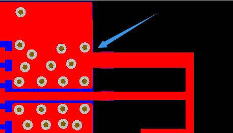
3. Pay attention to the Ground Stitching Vias
Place stitching vias along the edge of the ground plane nearest to the antenna. Space them no more than 6 mm apart (approximately λ/20 at 2.4 GHz). These vias tie the ground layers together and prevent unwanted edge currents from radiating and interfering with the antenna signal. Without them, the PCB edge itself becomes an unintended radiator.
Guideline 2: Why Does Impedance Matching Matter in PCB Antenna Design?
You can have a perfectly designed PCB antenna, but if the energy from the transceiver cannot get into it cleanly, most of that energy bounces back. The product works poorly in the lab and fails at range.
Every Bluetooth and Wi-Fi transceiver IC has a 50-ohm antenna port. The trace connecting the IC to the antenna, and the antenna itself, must also present 50 ohms. When they do not match, power reflects back to the source instead of radiating into the air. This is called impedance mismatch, and it is one of the most common causes of short wireless range.
Designing the RF Feed Line
The trace from the transceiver’s RF output to the antenna feed point is a transmission line. It must maintain 50 ohms along its entire length. There are two common structures:
Microstrip Line — a trace on the top layer, with a continuous ground plane on the layer directly below. The trace width for 50 ohms depends on the stackup:
| PCB Thickness (FR-4, εr ≈ 4.3) | 50-Ohm Trace Width |
|---|---|
| 1.6 mm (standard) | ~3.0 mm |
| 0.8 mm | ~1.5 mm |
| 0.4 mm | ~0.75 mm |
Coplanar Waveguide with Ground (CPWG) — a trace on the top layer, with ground pours on both sides on the same layer, plus a ground plane below. This gives better isolation and is preferred when the RF trace must run near digital signals or power traces.
The PI Matching Network: Your Insurance Policy
Even a perfectly laid-out feed line cannot guarantee that the antenna impedance will land exactly on 50 ohms after fabrication. Board material tolerances, nearby components, and the product enclosure all shift the antenna’s resonant frequency.
The solution is to include a three-element PI matching network between the transceiver output and the antenna feed — every single time, even if your simulation says the match is perfect.
The PI network consists of two shunt capacitors and one series inductor (or the reverse). You leave footprints for all three components on the PCB. You may or may not populate them, depending on what the VNA measurement shows after fabrication. If the antenna needs tuning, you add the calculated values. If not, you leave the pads open or install zero-ohm links.
Typical starting values for 2.4 GHz matching:
- Series inductor: 1–5 nH
- Shunt capacitors: 0.5–5 pF
A board respin to adjust antenna trace geometry costs money and time. Swapping a 0402 capacitor on a pre-designed footprint costs almost nothing.

Common RF Trace Mistakes
These layout errors cause impedance problems even when the trace width calculation is correct:
- 90° bends — the corner creates a capacitive discontinuity. Use 45° mitered bends or smooth arcs instead.
- Vias in the RF signal path — each via adds roughly 0.5–1 nH of parasitic inductance. Avoid them entirely in the feed line.
- Trace width changes — even a brief narrowing at a pad creates a mismatch point. Keep the trace width uniform from the IC pin to the antenna feed.
- RF trace over a ground plane split — the return current has no direct path, forcing it around the gap. This creates an impedance discontinuity and unexpected EMI.
Guideline 3: Where Should You Place the Antenna on the PCB?
Two engineers can build identical antennas. One product has 30 meters of range. The other barely reaches 5 meters. The only difference is where the antenna sits on the board.
Antenna placement controls how much of the antenna’s radiated energy reaches free space versus being absorbed or reflected by surrounding metal, components, and the product’s own ground plane. A well-tuned antenna in the wrong location will always underperform a simpler antenna placed correctly.
Place the Antenna at the Board Edge or Corner
This is the single most important placement rule. The antenna must sit at the edge or corner of the PCB. This gives the antenna access to free space in five of the six possible directions — up, down, and to three sides. The only blocked direction is back toward the board.
Placing an antenna in the center of the board surrounds it with copper on all sides. The ground plane and component metallization act as reflectors. The antenna radiates into the board instead of into the air. This mistake consistently produces 6–10 dB of gain loss compared to an edge-placed antenna.

Keep Metal Away from the Antenna
Metallic objects near the antenna absorb and reflect its radiated energy. They shift the resonant frequency and create nulls in the radiation pattern.
Minimum separation rules:
- At least 10 mm between the antenna and the nearest metallic component (shielding cans, connectors, coin cells, large capacitors)
- No switching power converter inductors or high-speed digital traces in the RF section of the board
- If a shield can is required, make sure the antenna sits outside it — never inside
The Enclosure Effect
The plastic enclosure around your product acts as a dielectric. It loads the antenna and shifts its resonant frequency downward — often by 50 to 100 MHz. This shift will move the antenna out of the 2.4 GHz band if it is not accounted for.
Always perform final antenna tuning with the enclosure in place. A board that tunes perfectly on the bench will detune when you close the case. Materials with a lower dielectric constant (such as polypropylene or PTFE) cause less shift than high-permittivity materials like ABS or polycarbonate. If you have a choice of enclosure material, choose one with a low permittivity.
Guideline 4: Does PCB Material Choice Affect Antenna Performance?
Many engineers select the PCB material based on cost and availability, not RF performance. This works — until it does not. At 2.4 GHz, the wrong material can make an antenna unmatchable or cause performance to vary unit-to-unit.
The substrate material controls three things that matter for antenna design: the effective dielectric constant (which sets the physical antenna length), the loss tangent (which controls how much energy is lost in the substrate), and the consistency of those properties from panel to panel.
FR-4: The Right Choice for Most 2.4 GHz Designs
Standard FR-4 (εr ≈ 4.2–4.6, loss tangent Df ≈ 0.02) works well for the majority of Bluetooth, BLE, Wi-Fi, and Zigbee products at 2.4 GHz. It is inexpensive, widely available, and compatible with standard fabrication processes.
The main limitation is variability. FR-4’s dielectric constant can shift by ±10% depending on resin content and glass weave orientation. For narrow-band antennas, this shift moves the resonant frequency enough to push it outside the target band. This is manageable with a properly designed matching network, but it means you should always plan for post-fabrication tuning.
When to Consider a Low-Loss Laminate
For designs operating above 5 GHz, or products with long RF feed lines where insertion loss matters, FR-4 is not the right choice. Low-loss laminates like Rogers RO4003C or RO3003 offer tighter dielectric constant tolerances and much lower loss:
| Parameter | FR-4 | Rogers RO4003C | Rogers RO3003 |
|---|---|---|---|
| Dielectric Constant (εr) | 4.2–4.6 | 3.38 ± 0.05 | 3.00 ± 0.04 |
| Loss Tangent (Df) | ~0.020 | 0.0027 | 0.0013 |
| εr Consistency | ±10% | ±1.5% | ±1.3% |
| Compatible with FR-4 Process? | Yes | Yes | No (PTFE-based) |
| Relative Cost | 1× | 5–8× | 8–15× |
Use Rogers or similar laminates when: your design operates at 5 GHz or above, your application requires tight unit-to-unit frequency consistency (e.g., phased arrays), or you are building for automotive or aerospace environments where material stability across temperature ranges is critical.
For cost-sensitive products that still need better RF performance than standard FR-4, a hybrid stackup is a practical solution — Rogers material on the outer layers where the antenna and RF traces are, and FR-4 on the inner layers for digital and power routing.
Recommended 4-Layer Stackup for Bluetooth / Wi-Fi Products
| Layer | Function | Notes |
|---|---|---|
| L1 (Top) | Antenna, RF traces, components | 50-ohm microstrip referenced to L2 |
| L2 | Ground plane | Continuous, no splits under RF section |
| L3 | Power plane | Adjacent to ground for decoupling capacitance |
| L4 (Bottom) | Signal routing | Keep digital traces here, away from RF |
Stitch the ground layers together with vias along all PCB edges, spaced no more than 6 mm apart.
Guideline 5: How Do You Test and Tune a PCB Antenna After Fabrication?
Simulation predicts what the antenna should do. Testing shows what it actually does. The difference between those two things is where most antenna problems live.
No PCB antenna design is complete at the layout stage. Material tolerances, nearby components, enclosures, and cable routing all shift the antenna’s behavior away from the simulation result. Testing and tuning close that gap.
Step 1: Measure S11 with a VNA
A Vector Network Analyzer (VNA) is the essential tool for antenna testing. It measures the S11 parameter (return loss) — the ratio of reflected power to incident power at the antenna input.
The target for a usable antenna is S11 ≤ −10 dB across the operating band (2.400–2.4835 GHz for Bluetooth and Wi-Fi). This means less than 10% of the power is reflected. A well-optimized antenna will reach −15 to −20 dB at the center frequency.
The VNA also shows the antenna impedance on a Smith chart. You can see directly how far the impedance is from 50 ohms and in which direction — too inductive, too capacitive, or too resistive — which tells you exactly what matching components to add.
Step 2: Calculate and Install Matching Components
If the S11 measurement shows the resonant frequency is shifted or the impedance is not centered:
- Read the impedance from the Smith chart at the target frequency.
- Calculate the matching component values needed to move the impedance to 50 ohms. An L-match (one series element plus one shunt element) corrects most cases. A PI network handles larger deviations.
- Install the calculated inductors and capacitors in the matching network footprints you left on the board.
- Re-measure with the VNA to confirm the result.
This process is fast — a single tuning session typically takes 30 to 90 minutes. Compare that to a full board respin, which can take weeks and cost thousands of dollars.
Step 3: Active Testing in Real Conditions
After the VNA confirms a good match, test the system actively — with the transceiver IC transmitting and receiving. Passive antenna tuning alone does not catch problems caused by:
- Switching regulator noise coupling into the RF section
- Display or CPU clock harmonics falling in the 2.4 GHz band
- Ground bounce from high-current digital loads
Use a spectrum analyzer to check for spurious emissions near the antenna frequency. Measure actual wireless range under operating conditions — not just in an open lab. For products requiring carrier approval, commission Total Radiated Power (TRP) and Total Isotropic Sensitivity (TIS) measurements in an accredited anechoic chamber.
EM Simulation Tools Worth Knowing
Before the prototype, simulation saves fabrication cycles. These are the tools used in professional PCB antenna design:
| Tool | Method | Best For |
|---|---|---|
| Ansys HFSS | Finite Element (FEM) | Full 3D antenna structures |
| CST Studio Suite | FDTD / FIT | Large board-level simulations |
| Sonnet | Method of Moments | Planar / microstrip antennas |
| MATLAB Antenna Toolbox | Parametric | Quick sweeps, PCB antenna prototyping |
Simulation should target S11 ≤ −10 dB across the band, radiation efficiency ≥ 50%, and an input impedance close to 50 + j0 ohms at the center frequency before cutting any boards.
How to Calculate PCB Antenna Dimensions for 2.4 GHz (Step by Step)
Knowing the math behind the antenna gives you the power to sanity-check any reference design — and to spot errors before fabrication.
Step 1: Calculate the free-space wavelength
λ = c ÷ f = 300,000,000 m/s ÷ 2,450,000,000 Hz ≈ 122.4 mm
Step 2: Calculate the quarter wavelength
λ/4 = 122.4 ÷ 4 ≈ 30.6 mm
This is the physical length of a quarter-wave monopole in free space. Texas Instruments’ application note AN058 confirms this figure.
Step 3: Apply the substrate shortening factor
On FR-4, the signal travels more slowly than in free space because of the dielectric. The effective dielectric constant of a microstrip on FR-4 is approximately 2.8–3.2, which shortens the physical antenna length to roughly 23–25 mm at 2.4 GHz. Use the impedance calculator built into your PCB design tool, or a dedicated RF calculator, to get the exact value for your stackup.
Step 4: Calculate the 50-ohm trace width
Use your PCB stackup data to calculate the microstrip width. For standard 1.6 mm FR-4 with εr ≈ 4.3 and 1 oz copper, the 50-ohm trace width is approximately 3.0 mm. For a 0.8 mm board, it is approximately 1.5 mm. Always verify these numbers against your manufacturer’s actual material data, not nominal values.

PCB Trace Antenna vs. Chip Antenna: Which One Is Right for Your Project?
This is one of the most common questions in PCB antenna design. The answer is not about which is better in the abstract. It depends on where your project is and what you are optimizing for.
| Factor | PCB Trace Antenna | Chip Antenna |
|---|---|---|
| BOM Cost | Near zero (copper trace only) | $0.15–$1.50 per unit |
| Board Area | Larger trace area required | Small component, but needs ground clearance |
| Design Effort | High — simulation, layout, tuning needed | Easier — swap the component or adjust matching |
| Sensitivity to Layout Changes | Very high — any board change may require re-tuning | Lower — component is pre-tuned |
| Post-Fabrication Tuning | Only via matching network; trace geometry is fixed | Easier — swap the component or adjust the matching |
| Best Phase to Use | Locked production designs in volume | Prototyping or designs with frequent changes |
The practical recommendation is this: start with a chip antenna during development. Lock the design and validate the enclosure. Then switch to a PCB trace antenna for the production run to reduce long-term BOM cost. The matching network footprints work for both approaches, so the transition does not require a board respin.
Most Common PCB Antenna Design Mistakes
These are the mistakes that IWDF Solutions sees most often when reviewing client PCB designs before fabrication. Each one has a direct, practical fix.
| # | Mistake | What Goes Wrong | How to Fix It |
|---|---|---|---|
| 1 | Antenna placed in the center of the board | Copper surrounds the antenna; radiation drops 6–10 dB | Move antenna to edge or corner |
| 2 | Copper under the antenna on inner layers | Detuned resonance, killed efficiency | Remove copper from keep-out zone on ALL layers |
| 3 | RF feed trace routed over a ground plane gap | Impedance mismatch; unpredictable EMI | Ensure continuous ground directly under the entire RF trace |
| 4 | No matching network footprints on the board | Cannot tune post-fabrication; full board respin required | Always include 3-element PI network footprints |
| 5 | 90° bends in the RF trace | Capacitive discontinuity; impedance mismatch | Use 45° mitered bends or smooth arcs |
| 6 | Switching regulators placed near the antenna | Digital switching noise couples into RF section | Keep noise sources at least 10 mm from the antenna area |
| 7 | Prototype built on different PCB material or thickness | Tuning results do not apply to production boards | Always prototype with production-identical material |
| 8 | Final tuning done without the enclosure in place | Enclosure shifts resonant frequency 50–100 MHz | Always tune with the enclosure closed and assembled |
Frequently Asked Questions
Q1: How do I design an antenna on a PCB?
Start by choosing the antenna type (IFA, MIFA, monopole, or chip) based on your frequency, size constraints, and development timeline. Calculate the physical antenna dimensions using the wavelength formula, adjusted for your substrate’s dielectric constant. Place the antenna at the edge or corner of the board, remove all copper from the keep-out zone on every layer, design a 50-ohm feed line, and leave footprints for a PI matching network. After fabrication, measure S11 with a VNA and tune the matching network until S11 is ≤ −10 dB across the target band.
Q2: What is the best PCB antenna for Bluetooth 2.4 GHz?
For most BLE and Bluetooth products, the Inverted-F Antenna (IFA) is the best starting point. It is compact, matchable, and widely documented in chipmaker reference designs from Silicon Labs, Nordic Semiconductor, and Texas Instruments. If space is the primary constraint, use a Meandered IFA (MIFA). For products still in active development with frequent design changes, a chip antenna reduces variables and speeds up the iteration cycle.
Q3: Does FR-4 work for 2.4 GHz antenna design?
Yes. Standard FR-4 is suitable for the vast majority of 2.4 GHz antenna designs. Its dielectric constant (εr ≈ 4.2–4.6) and loss tangent (Df ≈ 0.02) are acceptable at this frequency. The main issue is εr variability of up to ±10%, which can shift the resonant frequency of narrow-band antennas. A matching network handles this. For designs above 5 GHz, consider Rogers RO4003C or a similar low-loss laminate.
Q4: How large should the keep-out zone be for a 2.4 GHz PCB antenna?
For PCB trace antennas (IFA, MIFA, monopole), clear at least 15 mm on the same layer from the antenna trace to the nearest copper, and at least 6 mm on all other layers. For chip antennas, keep a 10 × 10 mm area free of copper on all layers beneath and around the component. These are minimums — more clearance always improves performance.
Q5: What is the minimum ground plane size at 2.4 GHz?
The ground plane should extend at least 31 mm (one quarter wavelength at 2.4 GHz) in the direction perpendicular to the antenna. The width should be at least equal to the antenna’s physical length. A ground plane shorter than this will detune the antenna and reduce bandwidth. For very small boards where this is not achievable, use a chip antenna with the manufacturer’s recommended layout, which is optimized for constrained ground plane sizes.
Q6: What does S11 mean in antenna testing?
S11 is the return loss parameter measured at the antenna input. It tells you how much of the signal power is reflected from the antenna instead of being radiated. An S11 of −10 dB means 10% of the power is reflected — this is the minimum acceptable threshold for most antenna designs. A good antenna will show S11 of −15 to −20 dB at the center frequency. You measure S11 with a Vector Network Analyzer (VNA), which also displays the antenna impedance on a Smith chart.
Q7: Can I use the same PCB antenna design for both Bluetooth and Wi-Fi at 2.4 GHz?
Yes, in principle. Both Bluetooth and Wi-Fi operate within the 2.400–2.4835 GHz band. A single well-designed IFA or MIFA can cover the full band for both protocols. However, if your product also needs Wi-Fi at 5 GHz, you will need either a dual-band antenna or two separate antennas with RF switching, because a single 2.4 GHz PCB trace antenna cannot efficiently cover both bands.
Conclusion
PCB antenna design comes down to five decisions: the ground plane, the impedance match, the placement, the substrate material, and the testing workflow. Each one directly controls whether your wireless product delivers the range and reliability your users expect.
The guidelines in this article follow the order in which most antenna failures happen. Engineers get the ground plane wrong first. Then the impedance match. Then the placement. The material and testing steps follow naturally once the layout fundamentals are in place.
If you are building a Bluetooth or Wi-Fi product and want to avoid a costly board respin, apply these five guidelines in sequence. Leave matching network footprints on every design. Test with a VNA before you close the enclosure. And tune again after you close it.
At IWDF Solutions, our engineering team applies this exact workflow across hundreds of RF PCB design projects each year — from initial antenna selection and EM simulation through prototype testing and volume PCBA production. If you are sourcing a PCB design partner in China with hands-on RF experience, our team can review your antenna design before it goes to fabrication. Contact us to discuss your project.