

Printed Circuit Boards (PCBs) are the backbone of nearly every electronic product, from smartphones to satellites. As devices grow more powerful and compact, engineers increasingly turn to multilayer PCB stack-ups to achieve reliable performance. Yet, designing the right stack-up can feel overwhelming, especially for beginners. This guide breaks down the essentials, offering clarity for engineers, designers, and procurement professionals alike.
What is PCB stack-up?
A PCB stack-up refers to the arrangement of copper and insulating material layers that form a printed circuit board. At its core, the stack-up is a blueprint showing how multiple layers—signal, power, and ground—are organized.
A simple 2-layer PCB has a top copper layer, a bottom copper layer, and an insulating core. But as circuit complexity increases, more layers are required. Multilayer stack-ups may include 4, 6, 8, or even more than 12 layers. The arrangement matters because it influences electrical performance, manufacturing costs, and mechanical durability.
In short, a stack-up is not just about “how many layers” exist—it’s about how layers are placed relative to each other to optimize performance.

Why is a multilayer PCB stack-up important?
The stack-up design has a direct impact on key performance factors:
- Signal integrity: Proper layer placement reduces crosstalk and reflections, ensuring high-speed signals travel cleanly.
- Electromagnetic compatibility (EMC): Thoughtful stack-ups minimize radiation and susceptibility to noise.
- Power distribution: Dedicated power and ground planes deliver stable voltage across the board.
- Size and density: Multilayer designs allow engineers to pack more circuits into smaller spaces.
- Cost efficiency: A well-optimized stack-up can reduce material use and avoid overdesigning.
For industries like aerospace, medical devices, and automotive electronics, the right stack-up is critical for compliance, safety, and performance.
How many layers can a PCB stack-up have?
The number of layers in a stack-up depends on the application’s complexity:
- 2-layer PCB: Simple consumer electronics like remote controls.
- 4-layer PCB: Common for IoT devices, small industrial products, or mid-speed designs.
- 6–8 layers: Used in high-speed networking, embedded systems, and automotive applications.
- 10+ layers: Typical in servers, advanced computing, and aerospace systems where high data throughput and reliability are critical.
Modern technology allows for stack-ups of over 50 layers, but such boards are rare and extremely expensive. For most engineers, the sweet spot lies between 4 and 12 layers.


Why do we need multiple layers in a PCB?
At first glance, it may seem simpler and cheaper to use just a single-layer or two-layer PCB. However, as electronic devices become more compact and require faster processing, additional layers become essential. Here’s why:
- Higher circuit density
Modern products—like smartphones or automotive control units—require thousands of connections. A 2-layer board cannot accommodate this complexity without creating routing conflicts. Multilayer stack-ups allow engineers to “spread out” traces across several layers, avoiding congestion. - Improved signal quality
High-speed digital signals (e.g., USB 3.0, PCIe, DDR memory buses) are sensitive to interference. With multiple layers, designers can carefully place signal traces next to ground planes, reducing crosstalk and maintaining signal integrity. - Reliable power delivery
Multiple layers make it possible to dedicate full planes to power and ground. This results in more stable voltages across the entire PCB, especially critical in processors, FPGAs, and RF circuits. - Size and weight reduction
Adding more layers allows circuits to be more compact. For example, instead of using a huge 2-layer board, a 6-layer PCB can fit into a compact smartphone. - Thermal performance
Heat dissipation is easier to manage in multilayer boards, as copper planes help spread and balance thermal loads.
In short, multiple layers are not just about complexity—they are about ensuring reliability, performance, and miniaturization in modern electronics.
Power and ground layers in PCB stack-up
One of the most important features of multilayer PCBs is the dedicated power and ground planes.
- Power plane: A continuous copper layer that distributes voltage to all components. Instead of routing dozens of traces, the plane provides a low-resistance path, ensuring stable power delivery.
- Ground plane: A solid copper layer that acts as the reference for all signals. It absorbs noise, minimizes electromagnetic radiation, and helps control impedance.
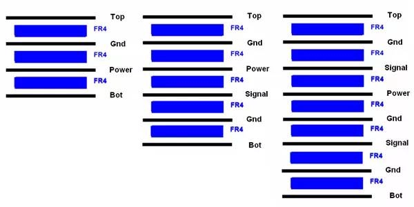
Advantages of using power/ground planes
- Lower noise: Planes reduce voltage drops and suppress electromagnetic interference.
- Better signal integrity: Signals running on adjacent layers benefit from a stable reference, reducing reflections.
- Simplified routing: Engineers don’t need to waste signal layers on power traces.
- Thermal management: Copper planes spread heat evenly across the board.
- Design flexibility: Multiple voltages (e.g., 5V, 3.3V, 1.8V) can be managed across different planes.
Without dedicated planes, engineers would struggle to design reliable high-speed or power-hungry circuits. That’s why at least one ground plane is standard in nearly all multilayer PCB stack-ups.
PCB stack-up design guidelines for design engineers
Designing a stack-up is part science, part art. While each project has unique requirements, here are some universal guidelines engineers should follow:
- Balance the stack-up
- Layers should be symmetrical to avoid mechanical stress.
- Example: A 6-layer board often uses [Signal–Ground–Signal–Power–Ground–Signal].
- Place ground planes strategically
- Always keep signal layers adjacent to ground planes.
- This minimizes loop area and reduces electromagnetic radiation.
- Control impedance
- High-speed signals require controlled impedance (like 50Ω single-ended or 100Ω differential pairs).
- Dielectric thickness and material properties must be chosen carefully.
- Minimize crosstalk
- Avoid placing parallel high-speed signals on adjacent layers.
- Use orthogonal routing (e.g., horizontal on one layer, vertical on another).
- Choose materials wisely
- FR-4 is common, but high-frequency circuits may require low-loss materials such as Rogers or Isola.
- Think about the manufacturing cost
- More layers mean higher costs.
- Aim for the minimum number of layers while maintaining performance.
- Consult with PCB manufacturers
- Every manufacturer has limits (minimum trace width, copper thickness, dielectric options).
- Always align your design rules with your fabricator’s capabilities.
For beginners, the key takeaway is: a good stack-up balances electrical performance, manufacturability, and cost.
PCB stack-up examples you can follow
To better understand how stack-ups are arranged, let’s look at some common industry examples.
- 4-layer PCB stack-up
- Top layer: Signal
- Inner layer 1: Ground plane
- Inner layer 2: Power plane
- Bottom layer: Signal
→ Widely used in consumer electronics and IoT devices. Balanced, cost-effective, and suitable for moderate-speed signals.
- 6-layer PCB stack-up
- Top layer: Signal
- Layer 2: Ground plane
- Layer 3: Signal (inner routing)
- Layer 4: Signal (inner routing)
- Layer 5: Power plane
- Bottom layer: Signal
→ Common in automotive, industrial, and networking equipment. Provides better signal isolation and routing space.
- 8-layer PCB stack-up
- Often arranged as alternating signal and plane layers.
- Example: Signal–Ground–Signal–Power–Ground–Signal–Power–Signal.
→ Used in high-speed computing, servers, and advanced communication systems.
Tip for beginners: Start by analyzing existing reference designs from PCB vendors. These examples save time and help avoid mistakes.
Using a PCB stack-up calculator effectively
Designing multilayer boards often requires precise impedance control. This is where stack-up calculators come in handy.
A stack-up calculator allows engineers to:
- Enter parameters like copper thickness, dielectric constant, and trace width.
- Simulate impedance values for single-ended and differential pairs.
- Adjust layer spacing and material choices to meet design requirements.
Popular tools include:
- Manufacturer-provided calculators (many PCB fabricators have online tools).
- Advanced software like Polar Instruments or integrated calculators in Altium Designer, KiCad, or Cadence Allegro.
How to use them effectively:
- Start with your PCB manufacturer’s standard material library.
- Input your planned trace width and spacing.
- Adjust dielectric thickness until impedance targets (e.g., 50Ω single-ended, 100Ω differential) are achieved.
- Validate results with your manufacturer before finalizing.
Using a calculator isn’t just about math—it’s about ensuring your design is manufacturable and reliable in real-world conditions.

Common mistakes in multilayer PCB stack-up design
Even experienced engineers can make errors when planning stack-ups. Here are some of the most frequent pitfalls:
- Unbalanced layer distribution
- Placing more copper on one side can cause warping during fabrication.
- Always aim for symmetry.
- Neglecting ground planes
- Using too few ground planes leads to noise and EMI problems.
- High-speed designs should always have at least one continuous ground plane.
- Improper signal routing
- Running parallel signals across adjacent layers increases crosstalk.
- Orthogonal routing is recommended.
- Ignoring manufacturing constraints
- Designing with trace widths or dielectric thicknesses that your fabricator cannot produce will delay or even cancel your project.
- Over-designing
- Adding more layers than necessary increases cost and complexity.
- Optimize for performance, not just “more is better.”
- No early communication with PCB vendors
- Failing to check with your manufacturer about stack-up feasibility often leads to redesign.
- Collaboration from the start saves time and money.
By avoiding these mistakes, even beginners can create robust, cost-effective multilayer PCBs that perform well in demanding applications.
How to optimize stack-up for signal integrity & EMC
Signal integrity (SI) and electromagnetic compatibility (EMC) are two of the biggest concerns in multilayer PCB design. A poorly designed stack-up can lead to timing errors, noise, or even product failure in compliance testing. Here’s how to optimize:
- Keep signals close to ground planes
- Place high-speed signals adjacent to ground planes.
- This ensures controlled impedance and reduces electromagnetic radiation.
- Use power–ground plane pairs
- A power plane next to a ground plane creates a natural capacitor.
- This stabilizes power delivery and suppresses high-frequency noise.
- Separate noisy and quiet circuits
- Keep analog and digital sections isolated.
- Provide separate ground planes if necessary, but connect them at a single point.
- Control return paths
- Ensure every high-speed signal has a direct return path through a nearby ground plane.
- Broken return paths cause loop areas, increasing EMI.
- Follow orthogonal routing
- On adjacent signal layers, route traces at 90° angles to each other.
- This reduces coupling and crosstalk.
- Choose materials carefully
- For very high frequencies (>1 GHz), low-loss laminates like Rogers or Isola are recommended.
- Standard FR-4 works well for most mid-speed applications.
Optimizing for SI and EMC is not optional—it’s essential for passing CE, FCC, or automotive EMC compliance tests required in Europe and the U.S.

Best practices for procurement managers and product managers when evaluating PCB stack-up
While engineers focus on design, procurement, and product managers also play a role in ensuring the right PCB stack-up is chosen. Here are best practices from a business and quality perspective:
- Request stack-up documentation
- Ask manufacturers to provide detailed stack-up drawings with dielectric thickness, copper weights, and materials.
- This helps verify the board meets design and compliance requirements.
- Evaluate cost vs. performance
- More layers increase costs significantly.
- Managers should balance product requirements against budget and volume expectations.
- Check material availability
- Some exotic laminates may be unavailable locally, leading to long lead times.
- Confirm that suppliers can source the specified materials reliably.
- Consider long-term reliability
- In industries like automotive or aerospace, PCBs must last for decades.
- Ensure the chosen stack-up has proven reliability under thermal cycling and vibration.
- Collaborate early with design teams
- Early alignment avoids surprises during manufacturing.
- Procurement managers should review stack-ups alongside engineers before final approval.
By following these practices, managers ensure that products are cost-effective, reliable, and manufacturable at scale.
Summary
Multilayer PCB stack-up design is the foundation of modern electronics. From defining how signals flow to ensuring EMC compliance, the stack-up impacts both performance and cost. By understanding its principles—whether you are an engineer, beginner designer, or procurement manager—you can make smarter decisions. Master the basics, avoid common mistakes, and always work closely with your PCB manufacturer to achieve the best results.