

PCB prototyping doesn’t have to be a bottleneck. By following a structured nine-step process, you can smoothly transition your design from concept to mass production—avoiding costly errors and delays.
This guide outlines the proven workflow used by expert B2B manufacturing teams worldwide. It tackles common pain points like design manufacturability, component sourcing, quality verification, and scaling from prototype to full production. Adopt this approach to cut down on redesigns, reduce scrap rates, and build a foundation for reliable manufacturing partnerships.
Step 1: Requirements Collection & DFM Consultation
The foundation of every successful PCB project begins with a comprehensive requirements collection phase. This is where strategic planning intersects with technical precision. During this critical first step, you’ll establish detailed specifications that directly influence every subsequent manufacturing decision.
Begin by scheduling an in-depth consultation with your manufacturing partner’s engineering team. This isn’t merely a formality—it’s where design constraints meet manufacturing capabilities. Your engineering team should clarify:
- Electrical requirements: Signal frequencies, power distribution needs, current-carrying capacity, impedance control specifications, and thermal dissipation requirements
- Physical constraints: Dimensional limitations, component placement restrictions, connector positions, and mechanical mounting requirements
- Environmental conditions: Operating temperature ranges, humidity exposure, vibration resistance, altitude compatibility, and chemical exposure potential
- Reliability standards: Whether the application requires aerospace (AS9100), automotive (AEC-Q100), medical (IPC-6012 Class 3), or industrial-grade compliance
Design for Manufacturability (DFM) principles should be integrated from this initial phase. DFM comprises two interconnected methodologies: Design for Fabrication (DFF) and Design for Assembly (DFA). Rather than treating these as afterthoughts, incorporating them upfront prevents expensive redesigns. A thorough DFM consultation identifies potential manufacturing obstacles before design commences, typically reducing overall project timelines by 20-30% and preventing costly rework later.
Your manufacturing partner will conduct a preliminary design review of your schematic to assess feasibility against their specific fabrication capabilities, equipment limitations, and material inventory. This consultation should address trace width capabilities (typically 6-8 mils for standard boards), via size minimums (0.3mm for cost-effective drilling), component footprint standards, and layer stack-up possibilities. Early identification of challenging design elements allows for proactive problem-solving rather than reactive crisis management when problems emerge downstream.

Step 2: Schematic & Layout Design
Once requirements are finalized, the detailed design phase begins with schematic capture and PCB layout optimization. This step is where theoretical specifications become a physical reality through careful circuit design and intelligent board layout.
During schematic development, designers must maintain strict adherence to DFM principles across three critical phases: the design phase itself, the component placement phase, and the routing phase. Each phase presents distinct manufacturability challenges that require proactive management.
Layout optimization extends beyond simple component placement. Signal integrity demands careful consideration of trace routing patterns, particularly for high-speed signals where trace length matching, impedance control, and electromagnetic compatibility become paramount. Power distribution must be strategically planned to minimize voltage drops and ensure stable power delivery across the board. Many design failures stem not from electrical theory but from oversight in practical layout considerations.
Critical layout elements include:
- Trace routing strategy: Separating signal layers from ground planes, maintaining consistent trace widths, avoiding sharp angles (45-degree turns preferred over 90-degree corners), and planning copper return paths to minimize loop inductance
- Via placement: Strategic via positioning for thermal management, signal connectivity, and ground distribution. Via sizes must balance thermal performance with manufacturing cost
- Component spacing: Maintaining adequate clearance between components for automated assembly (typically 0.2mm minimum between components), solder mask application, and potential rework scenarios
- Thermal management: Deliberate placement of thermal vias under high-power components, copper plane distribution for heat spreading, and consideration of component orientation for heat dissipation
For complex design challenges involving high-speed signaling, controlled impedance requirements, or demanding thermal scenarios, your manufacturing partner can provide specialized engineering support. Many manufacturers offer design assistance services that help optimize layouts for both electrical performance and manufacturing efficiency, often identifying opportunities to reduce costs while improving reliability.


Step 3: BOM Preparation & Validation
The Bill of Materials (BOM) serves as the critical interface between design intent and manufacturing reality. A poorly prepared BOM introduces procurement errors, delays assembly, increases costs, and can derail entire production schedules. Conversely, a meticulously validated BOM streamlines sourcing, prevents component obsolescence disasters, and reduces procurement timelines significantly.
Effective BOM preparation requires precision and foresight. Each component entry must include:
- Part number and manufacturer: Specify exact manufacturer part numbers rather than generic descriptions
- Quantity requirements: Account for prototyping needs (typically 10% excess for testing), small-batch production, and projected full-scale volume
- Component specifications: Detailed electrical specifications, package types (0603, 0805, BGA, etc.), and operating temperature ratings
- Environmental requirements: For automotive applications, AEC-Q100 certification is often mandatory. Military applications may require MIL-PRF specifications
- Packaging and lead time information: Critical for supply chain planning, particularly given that lead times for specialized components can reach 20 weeks
BOM validation goes substantially beyond simple component verification. It requires:
Component availability analysis: Verify that specified components remain in active production and aren’t approaching end-of-life (EOL) status. A component approaching obsolescence can create cascading supply chain disruptions. Many supply chain platforms now offer real-time component data indicating current availability, pricing, and lead time trends.
Alternative sourcing: Identify 2-3 qualified alternatives for each critical component. This redundancy proves invaluable when preferred suppliers experience allocation, preventing single-source dependencies that could halt production.
Cost optimization: Standard components with multiple manufacturers typically offer better pricing and availability than proprietary or specialty parts. A generic 1kΩ 0603 resistor sourced from multiple suppliers provides more flexibility than a specialized component from a single manufacturer. Strategic component consolidation—using identical values across the design wherever possible—reduces purchasing complexity and negotiating leverage improves.
Supplier collaboration: Proactive engagement with your PCB manufacturer allows them to identify potential sourcing issues before final design. Experienced manufacturers possess established supplier relationships, component intelligence, and material handling expertise that translates directly into faster sourcing timelines and cost optimization opportunities.
By thoroughly validating BOMs, you achieve a 90% reduction in procurement errors, 15-20% cost savings through alternative sourcing, and 30% faster supplier coordination. These improvements compound significantly when progressing to higher production volumes.

Step 4: Gerber/CAM Data Review
Gerber files and CAM (Computer-Aided Manufacturing) data represent the critical bridge between your PCB design and actual fabrication. Even minor errors at this stage can propagate through manufacturing, requiring expensive rework or board scrapping. Comprehensive data review according to industry standards prevents costly manufacturing delays and ensures first-pass manufacturing success.
IPC standards establish the framework for data validation. IPC-6012 defines the performance requirements for rigid PCBs, specifying electrical characteristics, mechanical tolerances, and reliability standards. IPC-A-600 provides visual acceptance criteria for finished boards. While your CAD software should automatically check against these standards, manual verification ensures nothing is overlooked.
Critical review elements include:
File completeness and accuracy: Gerber file sets must include all layers—copper layers (top, bottom, and internal), solder mask, silkscreen, drill files, and any specialized layers like controlled impedance or testing pads. Verify layer designations follow industry conventions to prevent layer misinterpretation.
Design rule verification: Confirm that trace widths meet manufacturing minimums (typically 6-8 mils for standard boards), clearance between traces exceeds manufacturer guidelines, via sizes accommodate drilling and plating processes, and no design elements violate the manufacturer’s specific fabrication capabilities.
Netlist verification: Cross-reference your CAM data against the electrical netlist to confirm connectivity integrity. This prevents shorts, opens, or misconnected traces that might not become apparent until electrical testing reveals failures.
Measurement and layer registration: Verify board outlines are precisely defined, tooling holes are clearly marked, and layer registration tolerances are achievable. Misaligned layers can compromise electrical performance, particularly in multi-layer boards where trace alignment is critical.
IPC-2581 format consideration: While Gerber files remain widely used, the newer IPC-2581 standard consolidates all design data—layer descriptions, assembly details, test specifications—into a single, standardized file format. IPC-2581 eliminates ambiguity inherent in multi-file Gerber transfers, reduces data interpretation errors, and accelerates CAM preparation, particularly for complex designs.
Modern manufacturers employ integrated DFM software that automatically validates your design against their specific fabrication rules and capabilities. This automated verification identifies potential manufacturability issues rapidly, often highlighting problems within hours rather than requiring manual engineering review spanning days.

Step 5: Prototyping Material Selection
Material selection profoundly influences PCB performance, manufacturing cost, and production feasibility. Different applications demand fundamentally different material properties. Selecting the appropriate substrate and copper thickness ensures your prototype performs as designed while maintaining cost efficiency and manufacturing practicality.
FR4 (fiberglass-reinforced epoxy) represents the most widely used PCB substrate, offering an optimal balance of cost, performance, and manufacturability. FR4 possesses:
- Dielectric constant (Dk) of approximately 4.5, providing stable electrical performance for general-purpose designs
- Glass transition temperature (Tg) of 130-140°C, adequate for most commercial and industrial applications
- Excellent mechanical strength and compatibility with standard fabrication processes
- Cost-effectiveness that makes it ideal for cost-sensitive applications
FR4 performs well for consumer electronics, industrial control systems, and standard automotive applications. However, extremely high-frequency designs or extreme temperature environments demand specialized materials.
High-frequency laminates (such as Rogers materials) offer dielectric constants optimized for RF and microwave applications, maintaining signal integrity at frequencies where FR4 becomes problematic. These materials reduce signal distortion and enable precise controlled impedance in communication and radar applications. However, they command significantly higher material costs—often 3-5x FR4 pricing.
Polyimide substrates excel in thermal resilience and mechanical flexibility, with glass transition temperatures exceeding 250°C, making them essential for aerospace, military, and extreme-environment applications. Their superior chemical resistance and radiation tolerance justify premium costs in mission-critical applications.
Copper thickness selection directly impacts electrical performance, current-carrying capacity, and thermal characteristics. Standard copper thickness is measured in ounces per square foot (oz/ft²):
- 0.5 oz (18 µm): Lightweight applications with minimal current requirements; cost-sensitive designs
- 1 oz (35 µm): Industry standard for most applications; adequate for typical commercial products
- 2 oz (70 µm): Power electronics, automotive applications, high-current circuits requiring lower resistance and superior thermal performance
- 3-4 oz (105-140 µm): Industrial and power distribution applications, extremely high-reliability circuits; heavy copper PCBs for specialized applications
Thicker copper reduces electrical resistance, minimizing voltage drops and power loss—critical considerations for high-current applications. Thicker copper also enables narrower trace widths while maintaining current-carrying capacity, optimizing PCB real estate. However, increased copper thickness affects manufacturing complexity and cost.
Your manufacturing partner should provide guidance on material selection based on specific application requirements, operating temperature ranges, signal frequency demands, and cost constraints. Early consultation prevents costly material substitutions during production or, worse, discovering performance inadequacy after prototypes are manufactured.

Step 6: Rapid Prototype Fabrication
Prototype fabrication transforms design files into physical circuit boards. Modern rapid fabrication processes prioritize speed without sacrificing quality, enabling product development cycles measured in days rather than weeks. Understanding fabrication technology and turnaround capabilities helps set realistic expectations and plan project timelines effectively.
Turnaround timelines vary based on design complexity:
- Simple single-sided or double-sided PCBs: 24-48 hours
- Standard 4-6 layer boards: 3-5 days
- Complex 8-12 layer boards: 5-7 days
- Advanced HDI (High-Density Interconnect) PCBs: 1-2 weeks
These timelines reflect concurrent manufacturing processes rather than sequential steps. Modern fabrication houses employ parallel production workflows where drilling, plating, and solder mask application proceed simultaneously whenever possible, rather than sequential processing that extends lead times.
Fabrication technology fundamentally impacts speed and precision. Laser Direct Imaging (LDI) systems replace traditional phototools by etching circuit patterns directly onto substrates using laser precision. LDI technology dramatically reduces pattern generation time, eliminates photomask creation delays, and enables faster setup for prototype runs. Additionally, LDI achieves superior precision compared to traditional phototool-based imaging, particularly critical for high-density designs.
Computer-controlled drilling and automated laser drilling systems ensure consistent hole positioning and diameter accuracy across entire boards. Automated plating processes maintain uniform copper distribution, preventing thickness variations that could compromise electrical performance.
Automated Optical Inspection (AOI) systems monitor fabrication in real-time, detecting defects during manufacturing rather than after completion. Proactive defect detection prevents entire batches from reaching completion with systemic defects, dramatically improving first-pass yields.
Material availability significantly influences turnaround. Manufacturers maintaining in-stock inventories of frequently used substrates (standard FR4, common layer counts, typical finishes) achieve faster production starts compared to custom material sourcing. When special materials like high-frequency laminates or specialized finishes are required, lead times typically extend proportionally to material sourcing time.
When selecting a manufacturing partner for prototyping, confirm their equipment capabilities align with your design requirements. Specialized designs demanding tight tolerance control, complex layer stackups, or exotic materials require partners with corresponding equipment investments and manufacturing expertise. Lower-cost facilities focused on high-volume standard boards may lack the capability for demanding prototypes.


Step 7: Testing & Quality Inspection
Comprehensive testing and quality verification represent the critical gateway between fabrication completion and prototype evaluation. Thorough testing identifies design flaws, manufacturing defects, and component quality issues before functional evaluation, preventing wasted development time on troubleshooting non-functional prototypes.
Electrical testing verifies connectivity, isolation, and basic electrical function:
- Continuity testing: Confirms that electrical paths between intended connection points exist with acceptably low resistance
- Isolation testing: Verifies that isolated circuits (such as different voltage domains) maintain adequate electrical separation, preventing shorts and cross-talk
- Flying probe testing: Mobile multi-point probes simultaneously verify multiple connection points, detecting opens, shorts, and improper connectivity rapidly
Automated Optical Inspection (AOI) employs high-resolution cameras and sophisticated image processing to examine PCB surfaces:
- Pattern verification: Confirming copper traces match design intent, missing traces are identified, unwanted copper bridges are detected
- Solder mask examination: Detecting mask defects, improper coverage, or erosion that could expose unintended copper
- Silkscreen verification: Confirming component labels and reference designations are correctly positioned and legible
- Dimensional verification: Measuring component pads, trace widths, and clearances to ensure compliance with design specifications
IPC-6012 Class requirements define acceptance criteria based on application type:
- Class 1 (General Electronics): Represents consumer electronics with non-critical applications; more permissive acceptance criteria
- Class 2 (Industrial/Commercial): Dedicated service equipment with extended reliability expectations; stricter requirements than Class 1
- Class 3 (High-Reliability/Aerospace/Medical): Mission-critical applications where continued high performance is essential; most stringent requirements including specialized testing, microsection analysis, and extensive documentation
Advanced inspection techniques employ sophisticated equipment for demanding applications:
- Automated X-ray Inspection (AXI): Provides visibility into hidden structures, including vias, BGA solder joints, and internal copper plating. Detects internal voids, insufficient plating, or hairline cracks invisible to optical inspection
- Microsection analysis: Cross-sections of representative samples to evaluate internal layer integrity, via plating quality, copper-to-dielectric adhesion, and structural soundness
- Functional testing: Actually powers the prototype and verifies that circuits perform as designed, identifying design errors that passed electrical connectivity tests but fail under actual operation
When specifying testing requirements, define the IPC-6012 Class appropriate for your application. Aerospace and medical applications typically demand Class 3 with extensive microsection analysis. Industrial equipment often requires Class 2. Consumer electronics typically specify Class 1. Aligned testing protocols ensure your prototypes meet reliability standards intended for production while avoiding unnecessary test costs when simpler verification suffices.


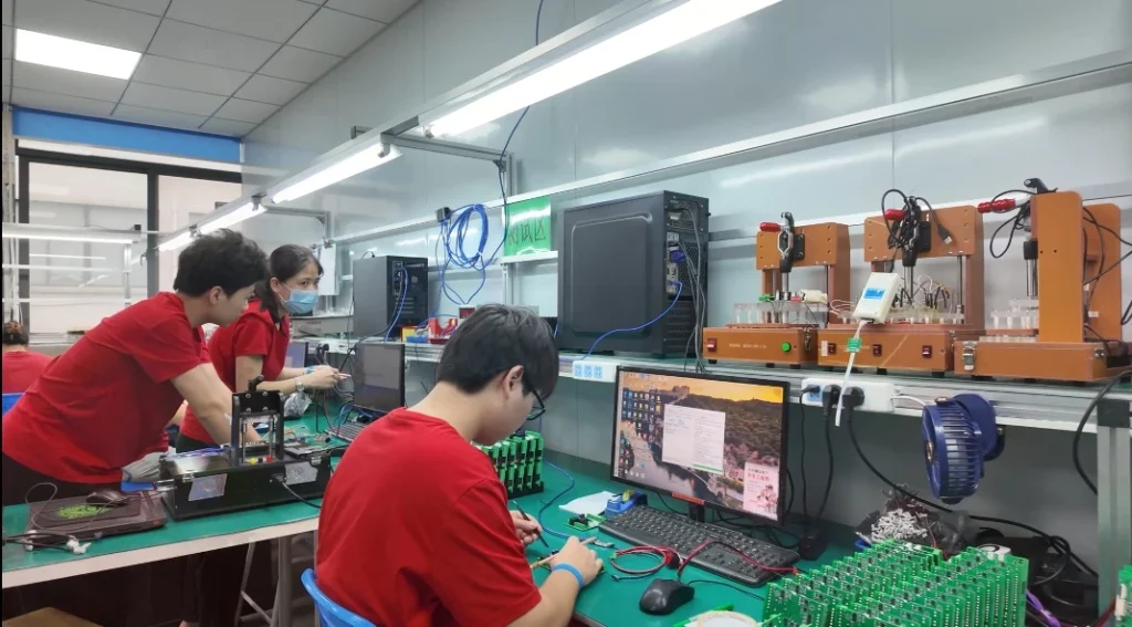
Step 8: Feedback & Iteration (Engineering Change Orders)
Rarely does a prototype perform perfectly on the first attempt. Design iteration based on prototype testing results represents the fastest pathway to optimized, reliable designs. Structured engineering change management ensures modifications are captured, documented, and validated before production transitions.
Engineering Change Orders (ECOs) provide formal mechanisms for documenting and implementing design modifications. Rather than haphazard design tweaking, structured ECOs create an audit trail documenting what changed, why changes were necessary, and when modifications occurred.
Common iteration triggers include:
Performance optimization: Testing reveals that performance approaches but doesn’t meet targets. Perhaps signal integrity exhibits marginal concerns, thermal management proves inadequate, or power consumption exceeds specifications. Design modifications addressing these issues—adjusting trace routing, modifying copper planes, adding thermal vias, optimizing component values—incrementally improve performance toward targets.
Component availability and cost: Original component choices may prove difficult to source or cost more than anticipated. ECOs facilitate substitution with alternative components offering better availability or pricing while maintaining equivalent functionality.
Manufacturing feasibility: Although DFM consultation helps identify manufacturability concerns early, unforeseen complications sometimes emerge during prototype fabrication. ECOs accommodate design modifications improving manufacturing efficiency—perhaps relocating components for better assembly automation, adjusting trace widths for cost reduction, or revising layer stackups for improved yield.
Reliability and longevity: Accelerated life testing or environmental stress screening might reveal marginal components, inadequate solder joint designs, or potential long-term reliability concerns. ECOs implement design corrections ensuring long-term reliability.
Structured iteration minimizes wasted modifications. Rather than implementing random changes hoping something improves, disciplined iteration involves:
- Analyzing test results to identify specific performance gaps
- Proposing targeted modifications most likely to address identified concerns
- Evaluating modification impacts on other circuit aspects, avoiding inadvertent side effects
- Implementing changes systematically with clear documentation
- Testing revised designs to confirm modifications achieved intended improvements
- Documenting all changes for production traceability and future reference
Modern design software enables relatively rapid ECO implementation. Changes to component values, footprints, or placement can be updated and regenerated in hours. However, layout modifications affecting trace routing, layer stackup, or board dimensions require more extensive rework. Prioritize ECOs addressing fundamental performance concerns over cosmetic improvements to maximize development velocity.
Your manufacturing partner can provide valuable guidance on iteration direction. Experienced engineers recognize patterns in prototype performance, suggesting modifications statistically most likely to address observed issues. Their insights compress iteration cycles, accelerating development.
Step 9: Transition to Mass Production
Successfully transitioning prototypes to mass production represents one of the most critical junctures in product development. A design performing perfectly at prototype scale may encounter unexpected challenges at volume. Systematic transition planning identifies and resolves scaling issues before full production commitments, preventing expensive rework or recalls.
Transition planning requires a detailed process definition addressing:
Design finalization and lock: Implement a formal design freeze, preventing further modifications once production planning commences. This control ensures manufacturing, supply chain, and quality teams all work from identical specifications. Design changes after production startup introduce chaos and error potential.
Pre-production validation: Execute small pilot production runs—typically 100-500 units—in actual production conditions using production equipment and processes. Pilot production identifies manufacturability issues, supply chain bottlenecks, quality concerns, and process optimization opportunities before full-scale production commitment.
Supply chain validation: Confirm component suppliers can reliably deliver required volumes within specified timelines. A component with 8-week lead times becomes problematic if production schedules demand 4-week replenishment cycles. Supplier qualification ensures consistency across multiple sources, preventing single-source dependencies.
Capacity verification: Confirm manufacturing partner possesses adequate capacity for projected production volumes. Overcommitting capacity leads to scheduling conflicts, delays, and quality degradation. Experienced manufacturers provide honest capacity assessments and timeline commitments.
Cost and lead time transparency: Establish clear pricing for production volumes, accounting for scaling advantages and material bulk purchasing benefits. Define realistic lead times based on production volume, component availability, and manufacturing capacity. Transparent communication prevents surprises when production launches.
Quality system transition: Production quality systems differ from prototype workflows. Production typically employs in-process quality verification, statistical process control, and automated testing rather than intensive manual inspection. Establish production quality criteria aligned with intended markets and application requirements.
First-article production: Before full production launch, manufacture and exhaustively test first articles using production processes and equipment. First-article inspection ensures production processes deliver equivalent quality to prototypes and confirms all design intent transfers correctly to production manufacturing.
Documentation completeness: Prepare comprehensive production documentation, including revised BOMs reflecting any ECO modifications, updated design files incorporating all iterations, manufacturing work instructions, quality acceptance criteria, test specifications, and traceability requirements.
Logistics and supply chain planning: Arrange component sourcing, material transportation, inventory management, and production scheduling. Complex supply chains for distributed manufacturing across multiple facilities require coordinated planning to prevent bottlenecks.
Typical transitions require 2-4 months from design finalization through pilot production validation to full-scale production readiness. Compressed timelines risk overlooking critical issues; extended timelines unnecessarily delay market entry. Your manufacturing partner should provide honest timeline guidance based on design complexity, component sourcing challenges, and production volume scale.
Why Choose IWDF Solutions for One-Stop PCB Prototyping?
IWDF Solutions specializes in exactly this journey—transforming design concepts into production-ready manufacturing realities. As a comprehensive one-stop PCB partner, IWDF Solutions combines design consultation, rapid prototyping, comprehensive testing, and volume production under a single oversight, dramatically simplifying your development process.
Key advantages include:
Integrated design engineering: IWDF’s design team collaborates with your engineers throughout the process, applying DFM principles from project initiation. This partnership prevents costly design errors, identifies manufacturability challenges early, and accelerates development timelines through proactive problem-solving rather than reactive crisis management.
Rapid prototyping capabilities: IWDF Solutions operates dedicated rapid-turn production lines utilizing laser direct imaging and automated processes, delivering functional prototypes within 24 hours for simple designs and 3-5 days for complex multilayer boards. This speed enables compressed iteration cycles and faster time-to-market.
Comprehensive testing and quality infrastructure: IWDF Solutions maintains state-of-the-art testing equipment, including automated optical inspection, electrical testing, X-ray inspection, and specialized testing for demanding applications. Rigorous quality protocols ensure prototypes meet your reliability standards.
Seamless prototype-to-production transition: Since IWDF Solutions manufactures both prototypes and production volumes, no handoff between vendors occurs. Design lessons learned during prototyping directly inform production processes, ensuring manufacturing consistency and quality continuity.
Material and component expertise: IWDF maintains extensive material inventories and established supplier relationships, enabling access to specialized substrates, exotic materials, and difficult-to-source components. This capability accelerates prototyping while avoiding supply chain delays.
Cost optimization through experience: IWDF identifies cost optimization opportunities during prototyping—material selections reducing costs without compromising performance, alternative components improving availability, and design modifications improving manufacturability efficiency. These improvements compound substantially when scaling to production volumes.


Frequently Asked Questions
Q: How long does the entire PCB prototyping process typically require?
A: Simple prototypes may be completed in 1-2 weeks from design submission through testing. More complex designs requiring multiple iterations typically require 4-8 weeks, depending on design complexity, iteration requirements, and component sourcing timelines. Transparent project planning identifies specific bottlenecks early, allowing timeline adjustments as needed.
Q: What constitutes a reliable PCB for high-reliability applications like aerospace or medical devices?
A: High-reliability applications typically require IPC-6012 Class 3 compliance, involving rigorous electrical testing, comprehensive visual inspection using IPC-A-600 standards, and microsection analysis verifying internal structural integrity. Material selection emphasizing proven aerospace-grade substrates, component qualification to specified standards, and extensive documentation creates the reliability foundation. IWDF maintains expertise in high-reliability manufacturing, possessing necessary certifications and experience.
Q: How much should I budget for PCB prototyping?
A: Prototype costs vary substantially based on design complexity, material selection, and required testing. Simple FR4 prototypes may cost $200-500 per unit. Complex designs with specialized materials, demanding testing, or expedited turnaround can reach $2000+ per unit. Volume discounts apply for pilot production runs. Early consultation with your manufacturer provides accurate budgeting based on your specific requirements.
Q: What’s the best approach to minimize expensive design iterations?
A: Comprehensive DFM consultation at project outset identifies potential manufacturing challenges, preventing costly downstream surprises. Rigorous design reviews catching errors before fabrication avoid expensive rework. Experienced manufacturing partners provide design guidance based on production realities, preventing academically correct but practically problematic designs. Structured iteration focusing on high-impact modifications achieves faster optimization than random design changes.
Q: How do I ensure my prototype will smoothly transition to production?
A: Prototyping should intentionally emphasize production-readiness rather than prototype expediency. Design choices should favor manufacturing processes available at the production scale. Component selections should balance prototype needs with production volume availability. Testing should verify production-equivalent performance. Early supply chain validation prevents sourcing surprises during production. Pilot production runs using actual production equipment and processes identify scaling issues early. IWDF’s integrated approach ensures prototype experience directly informs production processes, facilitating smooth transitions.
Q: How important is choosing the right material for my PCB?
A: Material selection fundamentally affects performance, reliability, cost, and manufacturing feasibility. FR4 provides excellent cost-performance for standard applications, but specialized materials become essential for extreme temperatures, high-frequency signals, or demanding reliability requirements. Your manufacturing partner should guide material selection based on application requirements and performance targets. Material decisions made early prevent expensive redesigns later.
Q: Can prototypes be manufactured quickly without sacrificing quality?
A: Yes—modern rapid fabrication technology enables quick turnarounds without quality compromise. Laser direct imaging, automated processes, and concurrent manufacturing workflows enable 24-48 hour turnarounds for simple designs while maintaining full quality verification. Comprehensive testing during prototyping identifies any quality issues immediately, preventing wasted time troubleshooting non-functional prototypes. Speed and quality are not mutually exclusive when working with experienced partners utilizing modern equipment.
Conclusion: Your Path to Manufacturing Excellence
The nine-step PCB prototyping process represents a proven methodology for transforming innovation into a reliable manufacturing reality. Each step builds upon previous work, progressively refining designs from conceptual intent to production-ready manufacturing specifications. By following this systematic approach, you dramatically reduce redesign cycles, identify and resolve challenges early when correction costs remain manageable, and establish strong foundations for long-term manufacturing partnerships.
The difference between a prototyping project that succeeds and one that consumes excessive time and budget often comes down to having the right manufacturing partner. IWDF Solutions combines technical expertise, modern equipment, and customer-centric service, transforming the prototyping journey from potential pain point into competitive advantage.
Your electronics deserve manufacturing partners who view prototyping as an investment in your success rather than transactional order fulfillment. IWDF Solutions stands ready to collaborate with your team, applying decades of cumulative manufacturing experience to accelerate your development, improve your designs, and establish manufacturing foundations supporting long-term growth.
Ready to transform your PCB concept into a manufacturing reality?
Contact IWDF Solutions’ engineering team today. Our PCB specialists are prepared to evaluate your project requirements, answer technical questions, provide comprehensive guidance, and deliver accurate proposals for prototyping and production. Whether your application demands rapid turnaround prototypes, high-reliability aerospace components, or cost-optimized volume production, IWDF Solutions possesses the expertise, equipment, and commitment to deliver exceptional results.
Reach out now for a free consultation. Let’s build something reliable together.