

Reverse engineering a PCB (Printed Circuit Board) is a fascinating process that helps engineers, hobbyists, and companies understand how a circuit was originally designed. Whether it’s for repairing old equipment, learning design practices, or creating compatible solutions, choosing the right software and tools makes the job much easier. This article will explore the best PCB reverse engineering software, tools, and techniques, while also covering important legal and practical considerations.

1. What Software Can Be Used to Reverse Engineer a PCB?
When it comes to reverse engineering, software is the most critical element. Specialized Electronic Design Automation (EDA) software allows you to recreate schematics, analyze layouts, and generate new design files from an existing PCB. Here are the most widely used options, with their pros and best use cases:
Altium Designer
- Best for: Professional engineers and enterprises
- Strengths:
- Industry-leading tool with advanced features for schematic capture and PCB layout.
- Excellent support for importing Gerber files, making it useful for reverse engineering.
- Strong library management, simulation tools, and 3D visualization.
- Why it’s good for reverse engineering: Altium allows precise recreation of board designs and is especially useful when working with complex, multi-layer PCBs.
- Downside: Expensive, making it less suitable for hobbyists.

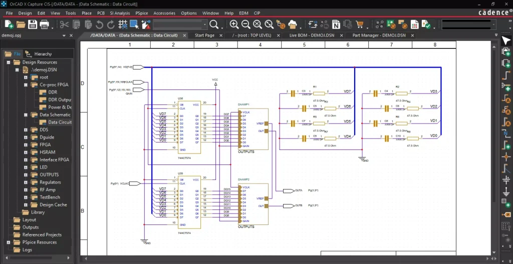
Cadence OrCAD
- Best for: Medium to large companies needing high accuracy
- Strengths:
- Robust simulation features (PSpice) for testing circuits.
- Reliable in generating netlists and recreating circuit behavior.
- Strong community and enterprise support.
- Why it’s good for reverse engineering: Particularly powerful when paired with schematic extraction workflows, allowing engineers to verify electrical functionality.
- Downside: Learning curve is steep, and licenses are costly.
Mentor Graphics PADS (Now Siemens EDA)
- Best for: High-level professional PCB engineers
- Strengths:
- Focus on signal integrity, high-speed design, and analysis.
- Advanced routing and netlist extraction tools.
- Why it’s good for reverse engineering: Excellent for high-performance boards where precision matters (e.g., telecom, aerospace).
- Downside: Complex tool, best for experienced engineers.
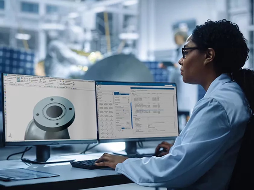
KiCad (Free, Open-Source)
- Best for: Beginners, hobbyists, and students
- Strengths:
- 100% free and open-source.
- Supports importing PCB images or scans to help rebuild layouts.
- Large online community with tutorials and plugins.
- Why it’s good for reverse engineering: Allows affordable entry into reverse engineering; useful for learning PCB structure before moving to professional tools.
- Downside: Limited advanced features compared to paid software.

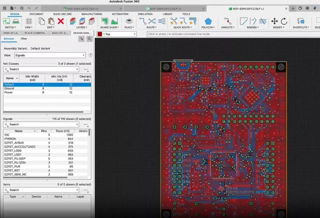
Eagle (by Autodesk)
- Best for: Makers, startups, and small businesses
- Strengths:
- Integrated with Autodesk Fusion 360, connecting PCB design with mechanical CAD.
- Widely used among hobbyists and DIY engineers.
- Why it’s good for reverse engineering: Good balance between ease of use and capability. Supports Gerber editing and schematic recreation.
- Downside: Subscription-based model, limited scalability for enterprise-level work.
CAM350 (Gerber Analysis Tool)
- Best for: Gerber file verification and analysis
- Strengths:
- Specializes in analyzing, editing, and verifying Gerber files.
- It can generate netlists, making it useful for schematic reconstruction.
- Why it’s good for reverse engineering: A must-have if your reverse engineering starts with Gerber files instead of a physical PCB.
- Downside: Not a full PCB design tool; works best alongside other EDA software.

Comparison Summary:
- For professionals/enterprises: Altium, OrCAD, PADS
- For hobbyists/students: KiCad, Eagle
- For specialized Gerber analysis: CAM350
This mix ensures there’s a solution for every budget and project type.
2. Key Features to Consider When Choosing the Software
When selecting PCB reverse engineering software, consider the following features:
- File Compatibility: Can the software import/export Gerber, ODB++, or CAD files? This is essential for working with manufacturing data.
- Ease of Use: Beginners will prefer tools with a gentle learning curve, while experts may prioritize advanced analysis.
- Schematic Capture: The ability to rebuild or recreate schematics from a PCB is crucial.
- Simulation & Testing: Features like PSpice or integrated circuit simulation help validate reverse-engineered designs.
- 3D Visualization: Viewing PCB layouts in 3D helps verify mechanical fit and component placement.
- Cost vs. Features: Free tools like KiCad are excellent for learning, but enterprises may require the advanced power of Altium or OrCAD.
- Community & Support: Open-source tools thrive on large communities, while professional tools come with official technical support.
3. What Tools Are Needed to Reverse Engineer a PCB?
While software is the brain of PCB reverse engineering, the right hardware and supporting tools act as the hands and eyes. Here’s a breakdown:
Hardware Tools
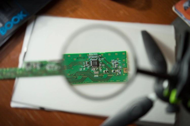
- Microscope
- Essential for inspecting fine-pitch components and tiny solder joints.
- Digital microscopes with USB connectivity let you capture images directly to your computer for analysis.
- Multimeter
- The most basic yet powerful tool.
- Allows continuity checks, resistance measurement, and identifying power rails or ground lines.
- Caliper
- Used for measuring board thickness, trace width, and component spacing.
- Important when redrawing the board in CAD to ensure accurate dimensions.
- Scanner or High-Resolution Camera
- A flatbed scanner or DSLR camera helps capture top and bottom layer images of the PCB.
- High resolution ensures trace visibility, which is crucial for later reconstruction.
- Desoldering Station
- Necessary when components block traces or vias.
- Allows careful removal of parts for full inspection without damaging the board.

Software Tools
- Gerber to Schematic Converters
- Tools like CAM350 or other Gerber viewers help analyze production files and sometimes extract a netlist.
- Image Editors (Inkscape, Krita, Photoshop)
- Useful for tracing PCB scans, color coding different layers, and aligning images before importing into CAD.
- CAD Viewers and Editors
- KiCad, Eagle, or Altium can accept your traced designs and let you rebuild a schematic and PCB layout.
Together, these hardware and software tools form the PCB copy toolkit. Beginners may start with just a multimeter, scanner, and KiCad, while professionals often combine advanced microscopes, desoldering stations, and Gerber tools for accuracy.
4. How to Reverse Engineer a PCB from Photos or Scans
One of the most accessible methods for beginners is reverse engineering a PCB using photographs or scanned images. Here’s a step-by-step guide:
Step 1: Capture Clear Images
- Use a flatbed scanner or DSLR camera to capture both sides of the PCB.
- Ensure the images are high-resolution (600 DPI or higher).
- If the components block traces, desolder them carefully and take another scan.
Step 2: Process the Images
- Import the images into image editing software (Inkscape, Krita, Photoshop).
- Adjust brightness/contrast to highlight traces.
- Align top and bottom layers using fiducial marks or mounting holes.
Step 3: Trace and Document Connections
- Use the software to digitally trace the copper paths.
- Label important pads (VCC, GND, signal lines).
- For double-layer or multi-layer boards, color-code each layer.
Step 4: Import into CAD Software
- Export your traced images and import them into KiCad, Eagle, or Altium.
- Place footprints for components and redraw the schematic.
- Use measurements (from calipers) to maintain scale accuracy.
Step 5: Reconstruct the Circuit
- From the schematic, generate a netlist.
- Verify connections using continuity tests with a multimeter.
- Compare with the original PCB functions to ensure accuracy.
Step 6: Verify and Test
- Once the schematic and layout are complete, use simulation tools (like PSpice in OrCAD or integrated simulators in Altium) to test the circuit.
- If possible, fabricate a prototype board to validate the reverse-engineered design.
5. Legal Considerations: Is PCB Reverse Engineering Allowed?
This is one of the most common questions engineers and companies ask before starting. The answer is: it depends on your purpose and jurisdiction.
Educational and Repair Purposes
- In many countries, reverse engineering for learning, academic research, or repair is generally allowed.
- Example: Repairing old industrial equipment by reconstructing an obsolete circuit board is often considered legal and necessary.
Commercial Duplication
- Copying a PCB for resale or commercial use without permission is usually illegal.
- This may violate intellectual property (IP) rights, patents, and copyrights.
- Large companies often protect their designs with NDAs (Non-Disclosure Agreements) and strict licensing.
Country-Specific Differences
- United States: Fair use allows reverse engineering in some cases, especially for interoperability or repair. However, commercial duplication without authorization is prohibited.
- European Union: EU law generally protects IP but allows reverse engineering for compatibility, research, and educational use.
- China & Southeast Asia: Enforcement varies; while duplication is common in local industries, global companies often pursue legal action if their products are copied.
Best Practice
If your goal is learning or repairing, you are usually safe. If your goal is mass production or commercial resale, always consult an IP attorney or get explicit permission from the original manufacturer.
Bottom line: Reverse engineering a PCB is legal in some contexts but illegal in others. Always be clear about your purpose.

6. Advanced Techniques and Professional Solutions
For hobbyists, a scanner and KiCad may be enough. But in professional settings, especially when working on complex multilayer PCBs, advanced techniques are essential.
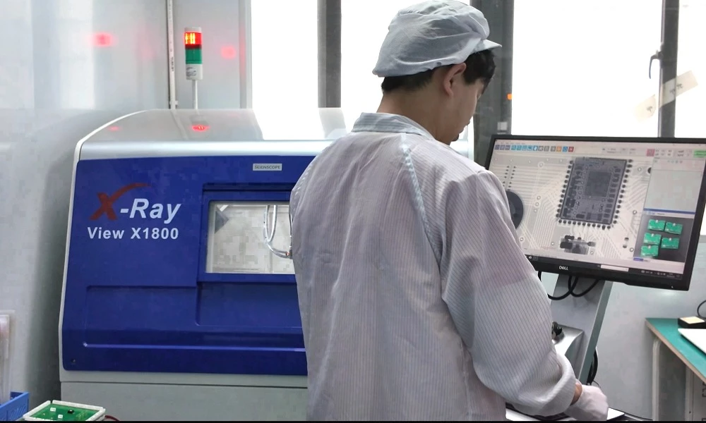
X-ray Inspection
- Used to see through layers of the PCB without destroying it.
- Helps analyze buried vias, internal traces, and BGA packages.
- Common in aerospace, defense, and high-reliability electronics.
3D Scanning
- Specialized 3D scanning equipment can create digital models of PCBs, including traces and component placements.
- Useful when working with mechanical integration (e.g., fitting a board into an existing device).
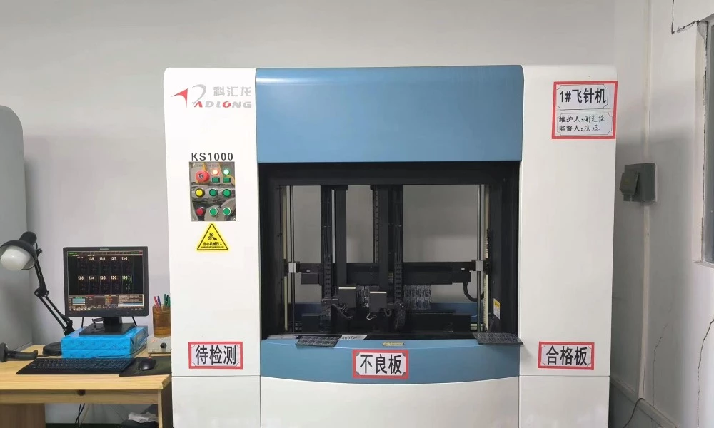
Automated Netlist Extraction
- Some professional tools can scan a board and automatically generate a netlist.
- This drastically reduces manual tracing time.
- Tools like Flying Probe Testers are often used in manufacturing and failure analysis.
High-End PCB Duplication Tools
- Companies specializing in reverse engineering often use dedicated PCB duplication software and hardware.
- These systems can create a nearly exact copy of an original board, including schematics, layouts, and BOM (Bill of Materials).
- Useful for industries where legacy equipment must be maintained, but original documentation is missing.
7. Free vs Paid PCB Reverse Engineering Solutions – Which Should You Choose?
Choosing between free and paid tools depends on your background, goals, and budget. Here’s a breakdown to help:
Free Solutions
- Examples: KiCad, Inkscape, Krita, Gerber file viewers
- Best for: Hobbyists, students, small DIY projects
- Pros:
- Zero cost and open-source flexibility
- Large online communities for support
- Great for learning the fundamentals of PCB design and reverse engineering
- Cons:
- Limited advanced features
- Slower workflow for complex multi-layer boards
- Requires more manual effort (e.g., tracing connections by hand)
Paid Solutions
- Examples: Altium Designer, Cadence OrCAD, Mentor Graphics PADS, CAM350
- Best for: Professional engineers, enterprises, mission-critical projects
- Pros:
- Robust advanced features (simulation, auto-routing, netlist extraction)
- Strong technical support and documentation
- Saves significant time on complex PCBs
- Cons:
- High cost (licenses can run thousands of dollars per year)
- Steeper learning curve for beginners
Which Should You Choose?
- Hobbyist/Beginner: Start with free tools like KiCad + image editors to build hands-on skills without investment.
- Professional Engineer: If precision, speed, and scalability matter, paid tools like Altium or OrCAD are worth the investment.
- Companies: Enterprises with legacy equipment or complex designs should combine paid EDA suites + advanced duplication tools for reliability.
In short, Free tools are excellent for learning, while paid tools are indispensable for professional and enterprise-level reverse engineering.
8. Conclusion & Key Takeaways
Reverse engineering PCBs is both an art and a science. The right combination of software and tools can turn a complex circuit board into a fully documented schematic and layout.
- Beginners can start with KiCad, Inkscape, and a scanner, while professionals should rely on Altium, OrCAD, or PADS for advanced projects.
- Essential tools like microscopes, multimeters, and Gerber analyzers make the process faster and more accurate.
- Methods like photo scanning, X-ray imaging, and 3D scanning open up possibilities for even the most complex PCBs.
- Always remember the legal considerations—reverse engineering for repair or education is usually fine, but commercial duplication can breach IP laws.
Whether you are a hobbyist learning PCB design or a company maintaining legacy equipment, selecting the right tools ensures accuracy, efficiency, and compliance.

