

In the intricate world of modern electronics, the printed circuit board (PCB) is the foundational bedrock upon which all functionality is built. While component selection and schematic design are critical, it is the physical implementation—the routing of copper traces—that ultimately determines a product’s performance, reliability, and manufacturability. PCB routing is no longer a simple task of connecting points A to B; it is a sophisticated engineering discipline that balances the often-competing demands of signal integrity, power delivery, thermal management, and the practical realities of mass production.
For global PCB designers, hardware engineers, and the procurement and technical personnel at EMS providers and OEMs, mastering trace design is non-negotiable. A poorly routed board can lead to signal degradation, electromagnetic interference (EMI), catastrophic power rail collapse, and thermal failures, resulting in costly re-spins, delayed time-to-market, and field returns. This guide is crafted to serve as a comprehensive, practical resource for professionals at all levels, from seasoned experts seeking a refresher on best practices to beginners building their foundational knowledge.
This article will systematically explore the principles and practices of effective PCB routing. We will dissect the fundamentals of signal and power integrity, delve into advanced techniques for high-density and high-frequency designs, and outline a robust design workflow that harmonizes electrical performance with Design for Manufacturability (DFM). Furthermore, we will provide actionable insights for selecting manufacturing partners and conclude with practical resources to streamline your design process. Throughout, we will focus on delivering actionable knowledge that can be immediately applied to your projects.
Foundational Principles of PCB Trace Design
Before diving into advanced techniques, a firm grasp of core principles is essential. These fundamentals form the bedrock upon which all successful high-density PCB designs are built.
1. Signal Integrity: The Cornerstone of Reliable Communication
Signal Integrity (SI) ensures that electrical signals transmitted from a driver are received at the destination without significant distortion. Key considerations include:
- Impedance Matching and Controlled Impedance: A trace is not just a wire; it is a transmission line. When a signal’s edge rate is fast enough (i.e., its frequency is high), the trace’s characteristic impedance becomes critical. Mismatched impedance between the source, trace, and load causes signal reflections, leading to overshoot, undershoot, and ringing. This is managed by designing the trace’s cross-section to a specific impedance value (e.g., 50Ω single-ended, 100Ω differential). The impedance is determined by the trace width, the height of the dielectric material to the reference plane, and the dielectric constant (Dk) of the material.
- Crosstalk: This is the unwanted coupling of energy from an “aggressor” trace to a nearby “victim” trace. It occurs through mutual capacitance and inductance. To minimize crosstalk:
- Increase the spacing between parallel traces. A good rule of thumb is 3x the trace width, but for sensitive signals, more is better.
- Use grounded guard traces between critical signals.
- Shorten the length over which traces run parallel to each other.
- Route sensitive signals on different layers and in orthogonal directions to minimize overlap.
- Return Path and Ground Plane Integrity: Every signal current traveling from a driver to a receiver must have an equal and opposite return current flowing back, typically through a ground plane. This return path seeks the path of least inductance, which is directly underneath the signal trace. A critical error is routing a signal trace over a split in the ground plane or changing reference planes without a nearby decoupling capacitor. This forces the return current to take a long, inductive detour, creating a large current loop that acts as an efficient antenna for EMI and degrades signal quality.


2. Power Delivery Network (PDN) Strategy
A stable power supply is as crucial as clean signals. The PDN must deliver a low-noise, stable voltage to all active components, even as their current draw changes instantaneously.
- Decoupling Capacitors: These are the first line of defense against power noise. They act as local, momentary energy reservoirs. Small-value capacitors (e.g., 0.1µF) handle high-frequency noise, while larger bulk capacitors (e.g., 10µF) handle lower-frequency current demands. They must be placed as close as possible to the power pins of the IC, with short and wide traces to minimize parasitic inductance, which renders them ineffective at high frequencies.
- Power Plane Stratification: In multilayer boards, dedicated power and ground planes are used. This creates a low-inductance, low-impedance power distribution system. The inherent plane capacitance also aids in high-frequency decoupling. A common stackup might alternate signal, ground, power, and signal layers to provide a consistent return path.
- Power Trace Separation: For lower-current rails that don’t warrant a full plane, use wide traces. A fundamental rule is to separate analog and digital power domains to prevent noise from the noisy digital section from coupling into the sensitive analog circuitry.


3. Layer Stackup and Its Impact on Routing
The PCB layer stackup is a strategic decision made before routing begins, as it dictates the electrical environment for all traces.
- Layer Spacing and Impedance: The pre-preg and core materials between layers define the dielectric height. Thinner dielectrics allow for finer trace widths to achieve a target impedance, but can increase crosstalk and cost. Your manufacturer can provide a controlled impedance stackup recommendation based on their materials.
- Via Selection: Through-Hole, Blind, and Buried:
- Through-Hole Vias traverse the entire board, are the least expensive, but consume space on all layers.
- Blind Vias connect an outer layer to one or more inner layers, but not through the entire board.
- Buried Vias connect inner layers without reaching the outer layers.
Using blind and buried vias (a technique known as High-Density Interconnect or HDI) frees up significant routing space on layers that don’t require the connection, which is essential for escaping fine-pitch BGAs and achieving high routing density. However, they add considerable cost and process complexity.

Practical Techniques for High-Density and High-Frequency Routing
As board real estate shrinks and signal speeds climb, routing becomes a more delicate art.
1. High-Frequency Impedance Control: Microstrip vs. Stripline
- Microstrip Lines: These are traces on an external layer, referenced to a single plane. They are easier to manufacture and have higher propagation speed but are exposed to external environmental factors and radiate more easily.
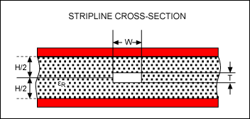
- Stripline Lines: These are traces embedded between two reference planes (typically power and ground) in an inner layer. They are shielded from radiation and external noise, leading to better EMI performance, but have a slower propagation speed and are more complex to fabricate due to tighter layer-to-layer registration requirements.

2. The Manufacturing Trade-Off: Width, Spacing, and Hole Size
Your design is constrained by your manufacturer’s capabilities. Communicate early and often.
- Trace Width/Spacing: Tighter traces and spaces allow for higher density but increase cost and the risk of etching defects and shorts. Standard capabilities for many manufacturers are 4/4 mil (milli-inch, or 0.1mm), but advanced shops can achieve 3/3 mil or lower. The appropriate trace width can be determined by using a dedicated PCB Trace width calculator.
- Aspect Ratio: This is the ratio of the board thickness to the diameter of a drilled hole. A high aspect ratio (e.g., 10:1) makes it difficult to plate copper evenly through the hole’s depth, risking reliability failures. A lower aspect ratio (e.g., 8:1) is more reliable.
3. Routing Topology and Strategy
- Straight and Direct Paths: Avoid 90-degree angles; they increase capacitance at the corner, which can cause slight signal reflections at very high frequencies. 45-degree angles are preferred.
- Differential Pairs: Routes must be of equal length and run parallel to each other, with consistent spacing throughout their length to maintain their differential impedance and reject common-mode noise. Any length mismatch must be corrected with a “tuning” section (serpentine) on the shorter trace.
- Critical Nets First: Always route sensitive clocks, high-speed serial links, and impedance-controlled nets first. Give them the most direct paths and cleanest return paths. Less critical signals like GPIOs can be routed in the remaining space.

4. Avoiding Common Pitfalls
- Acid Traps: Acute angles in traces can trap etching chemicals during manufacturing, potentially leading to trace corrosion and failure over time.
- Starved Thermals: In a thermal relief pad (a via or pad connected to a plane with “thermal spokes”), if the spokes are too thin or few, soldering can become difficult as the plane acts as a heat sink, leading to cold solder joints.
- Ignoring Thermal Pathways: Be mindful of component placement. Avoid routing sensitive signals directly under a component that is expected to generate significant heat, as the temperature change can affect the dielectric constant and thus the trace impedance.
A Co-Design Workflow for Signal Integrity and Manufacturability
A successful board is not just designed; it is engineered through a process that integrates simulation and DFM from the very beginning.
1. Integrating DFM and DFA
- Design for Manufacturability (DFM): This involves designing the board so it can be reliably and cost-effectively built. This includes adhering to the fabricator’s capabilities for trace, space, and hole size, providing adequate solder mask dams between pins, and ensuring uniform copper distribution to prevent warpage.
- Design for Assembly (DFA): This focuses on the ease of populating the board with components. It includes providing sufficient clearance for pick-and-place machines, standardizing component sizes where possible, and incorporating fiducial marks and tooling holes for accurate board alignment during assembly.
2. Pre-Layout Simulation and Verification
“Route and simulate” is more effective than “route and hope.”
- Pre-Layout SI Simulation: Use IBIS (I/O Buffer Information Specification) models to simulate signal quality for critical nets before routing. This helps determine the optimal topology (e.g., point-to-point, fly-by) and whether termination resistors are needed.
- Power Integrity (PI) Simulation: Analyze the PDN impedance across a frequency range. The goal is to ensure the PDN impedance is below a target threshold across all relevant frequencies, preventing rail collapse when the IC draws current.
- Thermal Analysis: Identify potential hot spots by simulating the power dissipation of components. This informs component placement and the need for heatsinks or thermal vias.


3. Post-Layout DFM and Impedance Checks
After routing, the design must be validated against manufacturing realities.
- Manufacturing Tolerances: Understand that a specified 50Ω impedance trace will have a tolerance (e.g., ±10%). Your design must be robust enough to function correctly within this window.
- Plating and Etch Factor: Copper plating in vias and etching of traces are not perfect processes. The “etch factor” accounts for the trapezoidal cross-section of a trace, which your manufacturer will consider in their impedance calculations.
- Testability: Include test points for critical signals and power rails to facilitate in-circuit testing (ICT) and debugging. Ensure they are accessible and not obscured by larger components.
Global Best Practices and Partner Selection
Different applications demand different design priorities, and choosing the right manufacturing partner is a strategic decision.
1. Application-Specific Design Preferences
- Consumer Electronics: Heavily biased towards cost reduction and miniaturization. Employs HDI techniques, fine-pitch components, and often operates at the limits of standard DFM rules.
- Industrial Control & Automotive: Prioritizes reliability and robustness under harsh conditions (vibration, wide temperature ranges). Uses thicker copper layers for higher current, wider trace spacing for improved reliability, and follows stringent standards like IPC-A-600 (acceptability of boards) and IPC-6012 (qualification and performance).
- Communication Equipment: The primary focus is on extreme signal integrity and impedance control, often using specialized low-loss RF materials (e.g., Rogers) mixed with FR-4. EMI control is paramount.


2. Selecting a PCB Manufacturer: Key Metrics
When evaluating an EMS or PCB fabricator, consider:
- Quality Certifications: Look for ISO 9001, IATF 16949 (automotive), and AS9100 (aerospace) as indicators of a mature quality management system.
- DFM/DFT Expertise: The partner should proactively provide detailed DFM feedback, not just a yes/no on your files. They should have the engineering capability to collaborate on complex stackup and impedance control.
- Global Supply Chain & Stability: A partner with a diversified global footprint (e.g., facilities in Asia, the Americas, and Europe) can mitigate regional supply chain disruptions and offer logistical advantages.
- Delivery and Service Commitment: Evaluate their on-time delivery record, communication responsiveness, and their ability to support you from prototype through volume production.
3. Fostering a Collaborative Partnership
Treat your manufacturer as a partner, not a vendor. Engage them during the design phase with your preliminary stackup and critical routing rules. Clear, complete documentation (Gerber, drill, netlist, IPC-356, and a detailed drawing) is essential to avoid misinterpretation and delays.


Practical Checklists, Resources, and Case Studies
1. Design Checklist: From Schematic to Layout
- Schematic:
- Decoupling capacitors are assigned to every power pin.
- Correct termination strategies are defined for high-speed nets.
- Stackup:
- Stackup defined with the manufacturer, with controlled impedance calculations.
- Symmetrical stackup to prevent warping.
- Layout:
- Critical high-speed nets were routed first with continuous reference planes.
- Differential pairs are routed with correct spacing and length matching.
- Decoupling capacitors are placed immediately adjacent to IC power pins.
- Power traces/planes sized for expected current.
- DFM rules (trace/space, hole size) verified against the manufacturer’s capabilities.
- Test points added for all critical nets.
2. Global Case Study Overview
A leading European automotive sensor developer faced signal integrity issues in a new, miniaturized radar module, leading to a 40% failure rate in initial prototypes. By collaborating with our global engineering team, we re-architected the 10-layer HDI stackup, implemented precise stripline routing for all critical analog sections, and added a comprehensive set of DFM rules for our fabrication line. The result was a first-pass-successful prototype, a yield increase to 99.2% in volume production, and a 30% reduction in board size, enabling the client to meet their aggressive performance and form-factor goals.
FAQ
Q1: How can I achieve stable impedance on a very small board with limited space?
A: Utilize HDI technology. Blind and buried vias allow you to create dense “localized” connections without consuming routing channels on every layer. This frees up space on critical layers to maintain consistent trace widths for impedance control. A carefully planned, multilayer stackup is essential.
Q2: What is the best practice for distributing ground planes in a complex multilayer board?
A: The ideal practice is to use unbroken, continuous ground planes. If you must split a plane for separate analog and digital grounds, do so only in one localized area. Route signals so they do not cross the split, and use a single “bridge” point (often a ferrite bead or a 0Ω resistor) to connect the two ground domains at one place to prevent a voltage differential from building up.
Q3: How many decoupling capacitors do I really need, and what values?
A: Use a combination. Start with a large bulk capacitor (e.g., 10µF) near the power entry point to handle low-frequency demands. Then, for each power pin on an IC, use a small-value capacitor (e.g., 0.1µF or 0.01µF) placed as close as physically possible. The small-value capacitor handles high-frequency transients. For very complex ICs like FPGAs, follow the manufacturer’s specific PDN recommendation.
Q4: My manufacturer asks for an “impedance coupon.” What is it?
A: An impedance coupon is a test structure included in the panel margins of your PCB. It contains traces fabricated with the same process as your actual board but are designed for easy probe access. The manufacturer uses these to physically measure the characteristic impedance of your design to ensure it meets your specified values, providing vital quality assurance data.
Conclusion
PCB routing is a complex but masterable discipline that sits at the intersection of electrical engineering, physics, and manufacturing pragmatism. By adhering to foundational principles, adopting a simulation-driven and DFM-focused workflow, and selecting a manufacturing partner with deep technical expertise and a global support structure, you can transform your high-density PCB designs from a source of risk into a competitive advantage.
Our global team provides a true one-stop solution, from collaborative design review and simulation support to high-yield manufacturing and rapid global logistics. We are committed to partnering with you to navigate the complexities of modern PCB design, ensuring your products are not only functional but also reliable, manufacturable, and successful in the market.
To access our downloadable design resources, receive a complimentary DFM analysis on your current design, or consult with our engineering team, please contact us today.