

The printed circuit board design software market has evolved dramatically over the past five years, with the global market expanding from $3.17 billion in 2023 to an estimated $4.63 billion in 2026, and projected to exceed $12 billion by 2033. This growth reflects the increasing complexity of modern electronics, the rise of cloud-based collaboration, and the integration of artificial intelligence into design workflows. Whether you are a hardware startup designing your prototype, an established electronics manufacturer scaling production, or a PCB design engineer evaluating new tools, selecting the right software can directly impact your project timeline, manufacturing costs, and product reliability.
This comprehensive guide explores the landscape of PCB design software available in 2026, explains how to evaluate tools based on your specific needs, and provides practical insights on integrating your design workflow with manufacturing partners like IWDF Solutions to achieve first-pass success.
What is PCB Design Software and how has it evolved by 2026?
PCB design software, also known as EDA (Electronic Design Automation) tools, encompasses the complete ecosystem of programs used to transform electronic concepts into manufacturable circuit boards. The core functionalities include schematic capture, which converts circuit diagrams into component symbols and electrical connections; PCB layout and routing, which places components and traces physical connections between them; design rule checking (DRC), which verifies compliance with manufacturing standards; simulation and analysis tools, which test signal behavior before fabrication; and documentation generation, which produces Gerber files, bills of materials (BOM), and assembly drawings required by manufacturers.
The evolution from 2020 to 2026 has introduced three transformative trends.
- First, cloud-based collaboration has become mainstream. Platforms like Altium 365, Autodesk Fusion, and EasyEDA enable distributed teams to work on the same design simultaneously, with real-time updates and version control—a critical capability for companies with engineering teams across multiple continents.
- Second, artificial intelligence and machine learning have begun automating repetitive tasks. Modern tools now offer AI-assisted component placement, automated critical net routing, and intelligent design rule suggestions that can reduce design cycles by 30 to 40 percent.
- Third, integration between mechanical and electrical design (ECAD-MCAD integration) has strengthened, allowing engineers to verify that PCB layouts fit within mechanical enclosures without back-and-forth conversions between software platforms.
Additionally, the industry has standardized around more robust file formats. While Gerber files remain the manufacturing standard, ODB++ and IPC-2581 formats provide richer design data, allowing manufacturers to extract more detailed information about design intent and manufacturing requirements directly from your files.

Key Factors to Consider When Choosing PCB Design Software in 2026
Picking the right PCB design tool isn’t just about features—it’s about matching the software to your actual needs, skills, and budget. Here’s a straightforward guide to help you decide, especially if you’re just getting started.
Start with Your Project’s Complexity
Not all projects need the same tool. Think about what you’re building:
- Simple boards – Like basic LED circuits, sensor modules, or single/double-layer PCBs. For these, free or low-cost tools such as KiCad, EasyEDA, or DipTrace are great choices. These tools offer sufficient routing capabilities, adequate component libraries, and DRC functionality without overwhelming the user interface.
- More advanced designs – Once you work with 4 or more layers, mix analog and digital signals, or need controlled impedance for faster signals, you’ll benefit from more capable software. Examples include motor controllers, embedded systems, or IoT devices with wireless connectivity. Here, tools like Altium Designer, Cadence Allegro PCB Designer, or Siemens Xpedition offer better control over high-speed routing, layer management, and design constraints.
- High-frequency or dense designs – If you’re working with RF, 5G, high-speed memory (like DDR), or miniaturized wearables, you’ll need professional-grade tools. These designs require precise impedance control, signal integrity analysis, and support for HDI or flexible PCBs. Allegro, Altium, and Siemens Xpedition are built for these challenges, though they come with a higher cost and steeper learning curve.
Why Impedance Control Matters
Impedance-controlled routing ensures signals travel cleanly without distortion—critical in high-speed or wireless designs. While tools like Altium and Allegro have this built in, KiCad users often handle it manually or with external calculators. If your design depends on reliable high-speed performance, choose software that simplifies impedance management from the start.
Keep It Practical
There’s no “best” software for everyone. Start with what fits your current project and skill level. You can always upgrade later as your needs grow. The goal is to spend less time fighting the tool and more time building great boards.
Team Size, Collaboration, and Cloud Integration
If your design team is co-located in a single office, desktop-based tools like Altium Designer or KiCad function perfectly well with minimal collaboration requirements. However, modern electronics companies increasingly operate with distributed teams across multiple time zones. In such environments, cloud-native or cloud-enabled platforms offer significant advantages.
Altium 365 excels in this area, providing a centralized workspace where team members can review designs, leave comments, access version history, and perform real-time concurrent editing. Autodesk Fusion also delivers strong cloud collaboration features, with desktop and browser-based access, allowing remote stakeholders to view and comment on designs without installing software. EasyEDA, being entirely browser-based, requires no installation whatsoever, making it ideal for rapid prototyping with distributed teams or when team members use various operating systems (Windows, macOS, Linux).
The advantage of cloud platforms extends beyond convenience. Version control integration, automated backup, and centralized access to component libraries reduce the risk of design data loss and ensure that all team members are working from the most current design files. For organizations managing multiple concurrent projects or maintaining design archives for regulatory compliance, this centralization provides significant operational efficiency.

Budget, Licensing, and Total Cost of Ownership
PCB design software spans an enormous price spectrum, from free open-source options to enterprise solutions exceeding $50,000 per year per user.
Free and Open-Source Options: KiCad, owned and maintained by the KiCad project, requires zero license fees. Over the past five years, KiCad has matured dramatically, offering push-and-shove interactive routing, hierarchical schematic support, 3D visualization, and libraries with hundreds of thousands of components. For startups, educational institutions, or companies designing boards with moderate complexity, KiCad represents compelling value. The trade-off is a steeper learning curve compared to commercial tools and a smaller community of professional users, making it harder to find experienced KiCad engineers in the job market.
Mid-Range Subscription Solutions: Tools like Autodesk EAGLE, DipTrace, and EasyEDA occupy the $50-300 per month range. These platforms provide production-ready features, intuitive interfaces, and reasonable component libraries. Autodesk EAGLE’s integration with Fusion 360 is particularly valuable if your projects require close mechanical-electrical coordination. DipTrace’s perpetual licensing option (pay once, use forever) appeals to companies preferring to avoid recurring subscription models.
Enterprise Solutions: Altium Designer, Cadence Allegro, and Siemens PADS typically operate on subscription models ranging from $300-600 per month per user. These platforms justify their cost through advanced features: comprehensive constraint management, integrated simulation, extensive component databases with supplier links, and professional-grade support. For organizations managing high-value programs (automotive, aerospace, telecom), the ROI on these tools is clear—a single design iteration saved in a project with millions of dollars at stake easily justifies the annual license cost.
When evaluating total cost of ownership, consider not just the license fee but also training costs, implementation time, and the cost of errors avoided. A design that fails DFM checks and requires expensive board respins in the middle of a manufacturing campaign represents a far greater expense than annual software licensing.
Manufacturing Handoff and Design-for-Manufacturability (DFM) Support
Getting Your Design Ready for Manufacturing (DFM)
A brilliant PCB design means nothing if it can’t be built properly. Your design software should help you bridge the gap between the digital layout and the physical factory floor. Think of it as preparing clear, complete instructions for your manufacturer.
1. Sending the Right Files
You’ll need to export your design into a format your manufacturer can use. While the traditional Gerber file is still universally accepted, sending more intelligent formats can prevent errors. Formas like ODB++ or IPC-2581 bundle everything—the copper layers, silkscreen, drill data, and even your component list—into one coherent package. It’s like giving the factory a detailed 3D model instead of just a set of 2D blueprints, helping them understand your intent and catch potential issues early.
2. Building Manufacturing Rules into Your Design Process
The real goal is to design with manufacturing in mind from the very first trace you draw. This is where modern software adds tremendous value.
Instead of finishing a design and then checking if a factory can make it, you should set your design rules upfront based on your chosen manufacturer’s capabilities. For example:
- They might require a minimum trace width of 4 mils for standard boards.
- For boards with very dense wiring, they might allow 3 mil traces.
- They will have specific rules for via sizes and the spacing between different elements.
Software like Altium Designer and Cadence Allegro lets you set these rules as guardrails before you even start routing. If you draw a trace too thin or place components too close, the software flags it immediately—just like a spell-checker for manufacturability. This prevents painful and expensive revisions later.
Key Takeaway: Use your design software not just as a drawing tool, but as a rule-checking partner. Configure it with your manufacturer’s specific requirements early on. This turns a final “DFM check” into a continuous, seamless part of your workflow, ensuring your design is buildable by the time you finish it.
Top 10 PCB Design Software Tools in 2026 (With Use Cases)
1. Altium Designer
Altium Designer remains the dominant platform for complex PCB design, favored by established electronics manufacturers and large design teams. The unified environment integrates schematic capture, PCB layout, design simulation, and documentation generation in a single application, eliminating the context switching required in tools that separate these functions.

Key Strengths: Altium’s differential pair routing with automatic length matching ensures signal integrity for high-speed interfaces. The component library management system is unmatched, integrating supplier pricing, stock availability, and lead time information directly into the BOM generation process—a capability that accelerates procurement and reduces component obsolescence risk. The 3D visualization is industry-leading, enabling engineers to verify that PCB layouts fit within mechanical enclosures before fabrication. Altium 365 cloud platform enables real-time team collaboration, version control, and design review workflows.
Typical Applications: Industrial automation controllers, telecom infrastructure, automotive electronics, medical devices, and high-performance computing boards where design complexity and reliability demands justify the tool investment.
Considerations: Altium is computationally intensive, requiring modern workstations with 16+ GB RAM for large boards. The learning curve is steep for newcomers; expect 2-4 weeks before becoming productive. Subscription costs are significant—plan for $400-500 per user annually. Considering that Altium Designer is a professional, paid tool with a significant learning curve, you can use whether a manufacturer actively employs it as a practical benchmark. Asking this question helps you gauge if they have the skilled team and depth of experience necessary to reliably handle complex designs.
2. Cadence Allegro PCB Designer
Allegro represents the highest tier of PCB design, purpose-built for the most complex applications in computing, telecom, and defense sectors.
Key Strengths: Allegro’s constraint management system is the gold standard. Engineers can define sophisticated routing rules—controlled impedance, length-matched differential pairs, crosstalk prevention, thermal management—and Allegro’s constraint solver automatically validates that these rules can be satisfied before routing begins. The tool supports server-class designs with thousands of nets and signal integrity analysis capabilities that predict behavior under real-world conditions. Allegro X (the latest version) integrates generative AI, enabling automated placement and routing suggestions that engineers can accept, refine, or reject based on design experience.
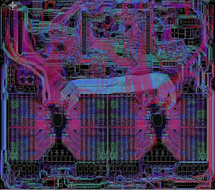
Typical Applications: CPU/FPGA motherboards, high-speed data center switches, 5G base station equipment, military radar systems, and aerospace avionics—applications where signal integrity and reliability are non-negotiable.
Considerations: Allegro has the steepest learning curve in the industry; many companies employ dedicated design teams that specialize in Allegro rather than asking general PCB designers to learn the tool. Implementation requires engaging Cadence professional services. Budget $800+ annually per user.
3. Siemens PADS Professional
Siemens PADS Professional is a mid‑ to high‑end PCB design platform aimed at small and midsize engineering teams that build industrial, automotive, and embedded control products but do not yet need a full enterprise EDA stack. It inherits much of the technology from Mentor Graphics while presenting a more accessible flow than heavy enterprise suites, which makes it attractive to companies transitioning from older tools and wanting a modern yet manageable environment.
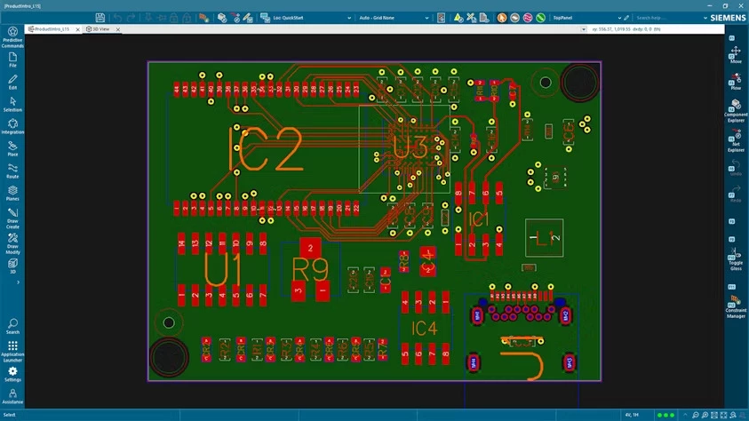
Key Strengths: PADS Professional offers powerful interactive routing with support for differential pairs, length matching, and constraint‑driven layout, allowing designers to implement high‑speed interfaces with predictable signal quality. Its automated design rule checking (DRC) engine continuously validates spacing, clearance, and manufacturing rules during layout rather than only at the end of the design, which reduces late‑stage surprises. Integration with HyperLynx provides strong signal integrity and power integrity analysis capabilities, enabling engineers to check reflections, crosstalk, and power distribution network behavior before committing to fabrication. The flow also connects to Valor for design‑for‑manufacturing analysis and manufacturing data preparation, helping teams generate production‑ready outputs with fewer manual steps.
Typical Applications: PADS Professional is well suited to complex industrial controllers, automotive electronic control units, power management boards, and multi‑board embedded systems used in factory automation or instrumentation. It fits teams that outgrew entry‑level tools like KiCad or Eagle but are not yet operating at the scale that justifies Xpedition or Allegro enterprise deployments. Many companies use PADS as a long‑term main tool for most products, while reserving more expensive enterprise platforms for only the most complex or safety‑critical programs.
Considerations: PADS Professional’s user interface, while more modern than legacy Mentor tools, can still feel less polished than Altium to some designers, particularly in terms of workflow smoothness and visual consistency. Cloud integration features are newer and generally less mature than those in Altium 365 or browser‑native tools, so organizations with heavily distributed teams may need to supplement PADS with external version‑control and collaboration systems. For organizations that eventually grow into very large, multi‑board and long‑lifecycle platforms, Siemens Xpedition provides a higher‑end upgrade path with more advanced enterprise features, while PADS Professional covers the needs of most mid‑size industrial and embedded design teams.
4. KiCad
KiCad‘s transformation from a hobbyist tool to a professional-grade platform represents one of the most significant developments in the PCB design landscape.
Key Strengths: Zero licensing cost makes KiCad attractive for startups and educational programs. The push-and-shove interactive router enables manual control over trace placement while simultaneously routing surrounding traces, a technique that professionals prefer over pure autorouting. Hierarchical schematic support allows breaking large designs into logical sub-circuits, improving maintainability. The 3D viewer is now production-quality, and the component library system supports unlimited custom components. Recent versions introduced footprint library linking, eliminating the historically complex symbol-to-footprint matching process.
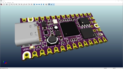
Typical Applications: Open-source hardware projects, educational institutions, small electronics companies, rapid prototyping environments, and companies where design complexity doesn’t demand the feature richness of enterprise tools.
Considerations: The community is smaller than Altium’s, making it harder to find experienced KiCad designers for hire. The learning curve remains steep, particularly for users transitioning from Altium. DFM support relies heavily on manual rule entry or third-party tools rather than integrated manufacturer rule libraries.
5. Autodesk EAGLE and Fusion 360
Eagle, now part of the Fusion 360 ecosystem, offers a middle ground between simplicity and capability.
Key Strengths: Fusion 360’s unique strength is seamless ECAD-MCAD integration. You can design a PCB in Fusion, then immediately view how it fits within a 3D mechanical enclosure, adjust component placement to accommodate mechanical constraints, and vice versa—all without switching applications. This tight integration is invaluable for consumer products where form factor and thermal management dominate design decisions. The browser-based Fusion interface enables collaboration without installation. Auto-routing capabilities are faster than legacy Eagle versions.

Typical Applications: Consumer electronics, wearables, IoT devices, and products where tight mechanical integration is critical.
Considerations: Fusion’s PCB features lag behind Altium in constraint management and signal integrity analysis. The free version of Eagle (browser-based) limits board size to 80×100 mm and 2 layers, restricting prototyping flexibility. Subscription cost is approximately $85-300 per month, depending on plan level.
6. EasyEDA
EasyEDA exemplifies the cloud-native approach to PCB design, eliminating the need to install anything beyond a web browser.
Key Strengths: True browser-based operation means zero installation, automatic cloud backup, and seamless access from any device. Real-time collaboration is built in—team members can view and edit simultaneously. The platform integrates real-time component pricing from major distributors, helping you validate design cost during the design phase. Simulation capabilities enable circuit testing before PCB layout.

Typical Applications: Rapid prototyping, PCB makers and small manufacturers, educational projects, and distributed teams where installation flexibility is valued more than advanced constraint management.
Considerations: Advanced features like hierarchical schematic capture and sophisticated impedance control are limited compared to Altium or Allegro. Export formats are adequate for manufacturing but lack the richness of ODB++ available in higher-tier tools. Free tier is quite capable, with premium tier at $50-100 monthly.
7. DipTrace
DipTrace occupies a unique market position: a perpetual-license, single-purchase model in an industry moving toward subscriptions.
Key Strengths: One-time purchase price ($500 for the professional version) eliminates recurring licensing costs, appealing to freelance designers and small companies. The interface balances power and usability well. Support for up to 32 copper layers accommodates complex designs. Drag-and-drop editing and graphical DRC reporting reduce the learning curve.
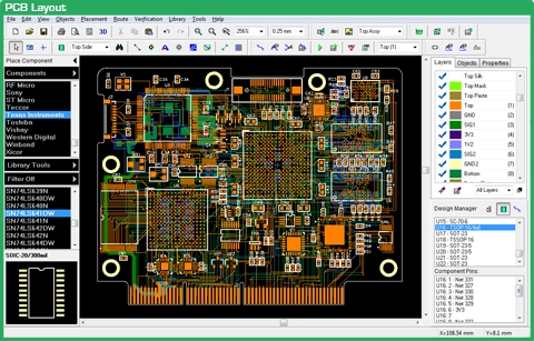
Typical Applications: Freelance PCB designers, small electronics companies, and established companies wanting to avoid subscription models.
Considerations: The user community is smaller, making online support and template sharing less robust than Altium. Component library management is manual, requiring more effort than automated systems. Export options are standard but less sophisticated than ODB++.
8. Zuken CR-8000
Zuken’s flagship tool addresses high-speed and high-reliability designs with sophisticated analysis capabilities.
Key Strengths: 3D PCB design modeling enables visualization of complex stackups and mechanical interactions. The concurrent design environment supports team-based workflows where different engineers work on sections of the same board simultaneously. High-speed features include transmission line analysis, eye diagram generation, and EMC simulation tailored for compliance verification.
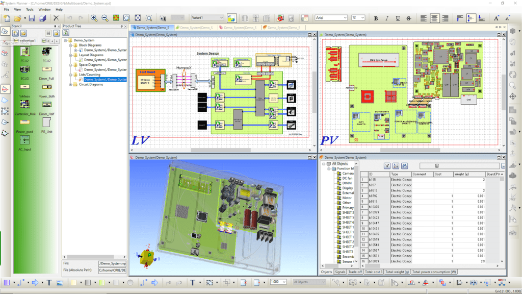
Typical Applications: Automotive electronics, aerospace systems, and high-performance computing where first-pass manufacturing success is essential.
Considerations: Zuken is primarily strong in Asia; support and adoption in North America and Europe are less widespread than Altium or Allegro. Implementation requires professional services. Licensing and support costs are premium-tier.
9. Siemens Xpedition
Siemens Xpedition is an enterprise‑class PCB design suite engineered for organizations that manage extremely complex, safety‑critical, and long‑lifecycle electronic systems. It provides a deeply integrated flow from system definition through schematic, layout, verification, and manufacturing preparation, which is why it is widely adopted by aerospace, defense, telecom, and automotive OEMs with strict process and compliance requirements.

Key Strengths: Xpedition offers a fully integrated, constraint‑driven design environment, where electrical, physical, and manufacturing rules are defined at the system level and enforced automatically during schematic capture and PCB layout. Real‑time DRC and advanced constraint management ensure that manufacturability, signal integrity, and reliability requirements are maintained throughout the design process rather than checked only at the end. The routing engine supports advanced high‑speed and mixed‑signal techniques, including complex differential pair topologies, length‑tuning for parallel buses, and intricate via and fan‑out strategies required in dense HDI and high‑layer‑count designs. Tight integration with mechanical CAD tools enables robust ECAD‑MCAD collaboration, allowing mechanical and electrical teams to co‑design enclosures, cooling paths, and board outlines with fewer iterations.
Typical Applications: Xpedition is typically deployed in large aerospace and defense programs, telecommunications infrastructure (e.g., base stations, core network equipment), and automotive OEM platforms that must remain in production and supported for 10 years or longer. These environments value Xpedition’s process control, data management, and multi‑discipline collaboration capabilities as much as they value its raw layout power. It is also favored where regulatory and quality standards demand traceable, audited design flows, such as ISO 26262 in automotive or DO‑254 in avionics.
Considerations: Implementing Xpedition is a significant organizational undertaking: it usually requires dedicated CAD administrators, formal training programs, and close cooperation with Siemens to configure flows, libraries, and data management to match company processes. Licensing is negotiated at the enterprise level rather than as simple per‑seat subscriptions, resulting in higher upfront and ongoing costs compared to mid‑range tools like PADS Professional or Altium Designer. For small teams or companies without highly formalized processes, Xpedition may be more tool than they can practically absorb, which is why many organizations treat it as the top of a tool ladder, moving to Xpedition only once their product portfolio and compliance requirements justify the investment.
10. Proteus PCB Design
Proteus PCB Design is a popular platform for combining schematic capture, PCB layout, and interactive circuit simulation in one environment, making it a common choice in universities, training centers, and small electronics companies. It is especially well-suited to projects where understanding the interaction between firmware and hardware is as important as producing a manufacturable PCB, which is why many teams use it as a bridge between education and professional development.
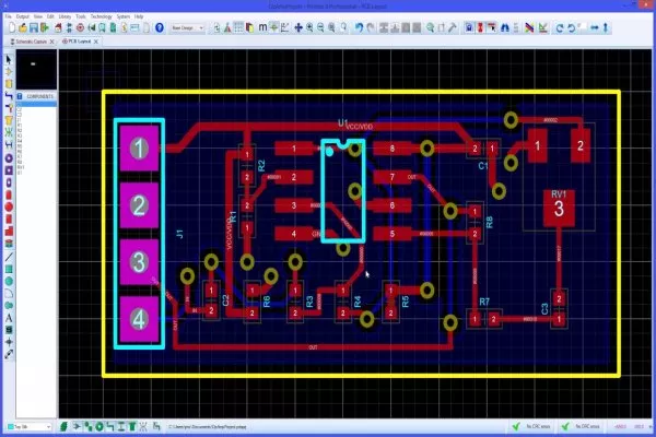
Key Strengths: Proteus is widely recognized for its ability to simulate complete microcontroller-based systems, including PIC, AVR, ARM Cortex-M, and Arduino-compatible devices, together with external peripherals, displays, and sensors. This allows engineers and students to validate both hardware topology and embedded code behavior before committing to physical prototypes, reducing the number of board spins and debugging cycles. The schematic and PCB editors are relatively easy to learn, with a clear user interface, integrated libraries for common components, and straightforward design rule checking that supports multilayer boards for low to medium complexity designs. Standard manufacturing outputs such as Gerber and drill files are supported, so once a design is verified in simulation, it can be exported and sent directly to a professional PCB manufacturer for fabrication and assembly.
Typical Applications: Proteus is widely adopted in electronics education programs, vocational schools, and training labs, where instructors need a single tool to teach circuit theory, embedded programming, and PCB implementation. Small hardware startups and project teams use Proteus for early-stage concept development, especially for microcontroller-based control boards, sensor modules, and simple communication interfaces where full enterprise EDA tools would be excessive. Engineering departments in larger organizations often rely on Proteus as a training and prototyping environment for junior engineers and interns, allowing them to complete end-to-end designs—from schematic and firmware to PCB layout—before migrating their workflows to higher-end platforms used on complex or safety-critical products.
Considerations: Proteus is not intended for very high-speed, high-layer-count, or highly regulated designs, and it lacks the advanced constraint management, signal integrity analysis, and impedance control capabilities found in platforms like Altium Designer, Cadence Allegro, or Siemens Xpedition. For projects involving dense HDI boards, 5G RF sections, or mission-critical automotive and aerospace electronics, teams typically outgrow Proteus and adopt enterprise-grade tools while continuing to use Proteus for teaching, early exploration, and microcontroller-centric prototypes. Cloud collaboration features and deep integration with enterprise PLM or version control systems are limited, so organizations with distributed, multi-site teams usually treat Proteus as a complementary tool rather than the backbone of their production design flow.
Comparative Feature Table
| Software | Best For | Complexity | Licensing Model | Cloud Collaboration | AI / Advanced Analysis | DFM Support | Typical Cost Level* |
|---|---|---|---|---|---|---|---|
| Altium Designer | Complex, multilayer, high‑speed industrial boards | High | Subscription (per user) | Very strong (Altium 365) | Growing AI-assisted routing | Strong, integrated | $$$ (premium) |
| Cadence Allegro PCB | Very complex, server/HDI, telecom, data center boards | Very High | Manual/basic | Enterprise workflows | Generative AI (Allegro X) | Strong, enterprise | $$$$ (enterprise) |
| Siemens PADS Prof. | Industrial, multi‑board systems, mid‑size design teams | High | Subscription | Moderate (newer cloud) | HyperLynx SI integration | Strong (Valor link) | $$$ (similar to Altium) |
| KiCad | Open‑source, SMBs, education, budget‑sensitive teams | Medium | Free, open‑source | Limited (via plugins) | None (external tools only) | Manual / basic | $ (free) |
| Autodesk Eagle/Fusion | Consumer/IoT, ECAD‑MCAD integration, small companies | Medium | Subscription | Strong (Fusion cloud) | Limited | Basic | $$–$$$ |
| EasyEDA | Browser‑based rapid prototyping, makers, small teams | Low–Medium | Subscription/enterprise | Excellent (cloud‑native) | Basic simulation | Basic (Gerber-level) | $–$$ |
| DipTrace | Subscription/enterprise | Medium | Perpetual + upgrades | Minimal | None | Basic | $$ (one‑time) |
| Zuken CR‑8000 | High‑speed/5G, automotive, complex RF/digital hybrids | High | Free/low-cost plans | Good (team workflows) | Strong SI/PI & EM analysis | Strong, integrated | $$$$ (enterprise) |
| Siemens Xpedition | Large aerospace, defense, telecom, long‑lifecycle OEMs | Very High | Enterprise (organization) | Enterprise‑grade | Advanced analysis & flows | Strong, integrated | $$$$ (enterprise) |
| Proteus PCB Design | Education, labs, MCU‑based prototypes, training usage | Low–Medium | Perpetual / subscription | Limited | Integrated circuit simulation | Basic (Gerber-level) | $$ (mid‑range) |
2026 Trends: AI, Cloud, and Industry-Specific Workflows
AI-Assisted PCB Design
Artificial intelligence integration into PCB design has progressed from speculative to practical. DeepPCB Pro, developed by InstaDeep in collaboration with Google Cloud, uses reinforcement learning to automate component placement and critical net routing, reducing design cycles by up to 30 percent. Users provide high-level constraints—”keep this power IC near these decoupling capacitors, maintain 50-ohm impedance for these traces”—and the AI generates placement and routing solutions that satisfy these constraints.
Cadence’s Allegro X AI takes a different approach, using generative models to propose multiple design candidates, enabling engineers to explore design space rather than committing to a single manual solution. Zuken’s CR-8000 2025 version now offers AI-assisted schematic annotation, reducing manual documentation time by up to 30 percent in testing.
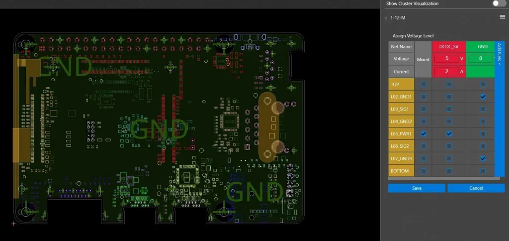
The practical impact: AI excels at optimizing known parameters (minimizing trace length, avoiding crosstalk, maximizing routing density) but cannot replace experienced design judgment for novel or safety-critical applications. The most effective approach treats AI as an assistant that accelerates routine optimization while engineers focus on novel challenges and design trade-offs.
Cloud-Based and Browser-Based PCB Tools
Cloud-native design platforms represent a structural shift in how electronics teams collaborate. Rather than managing files through email and version control systems, cloud platforms like Altium 365, Autodesk Fusion, and EasyEDA provide centralized workspaces where all stakeholders—designers, manufacturing engineers, procurement specialists, and project managers—access the current design simultaneously.
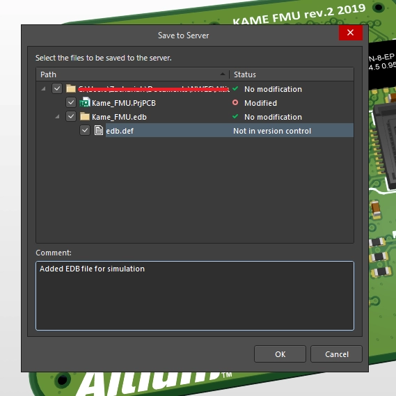
This architecture enables unprecedented transparency. When a design undergoes revision, all stakeholders see the change immediately rather than discovering it through delayed file sharing. Version history is automatic, with every change tracked and reversible. Comments and design reviews happen within the tool itself rather than through email threads scattered across inboxes.
For companies managing multi-site or international teams, cloud platforms eliminate timezone friction. A designer in London can leave annotated comments on a PCB layout; when the Shenzhen manufacturing team arrives in the morning, they see detailed context without requiring a synchronous meeting.
Industry-Specific Requirements in 2026
The era of “one-size-fits-all” PCB design is over. In 2026, design tools are evolving to tackle the unique, high-stakes challenges of specific industries head-on.
Automotive Electronics: The Compliance & Traceability Challenge
Modern vehicles are data centers on wheels. Designing for autonomous systems, battery management, or advanced driver-assistance (ADAS) isn’t just about circuitry; it’s about compliance. Strict standards like ISO 26262 for functional safety require you to document every design choice and prove its safety. Your software now needs to do more than draw traces—it must help build an auditable history. Tools like Allegro and Xpedition are responding with built-in automotive rule sets and documentation generators, turning a manual compliance headache into a managed part of the workflow. Long-term component sourcing (OEMs must support vehicles for 10+ years) is another layer, making library management a strategic task, not just an organizational one.
5G & High-Frequency: Where the Physics Dictates the Design
At millimeter-wave frequencies (like 28 GHz for 5G), a PCB is no longer just an electrical connector; it’s a precision waveguide. The materials themselves become part of the circuit. Every detail—from the substrate’s dielectric constant to the copper’s surface roughness—directly impacts signal loss and integrity. Your design tool must move beyond basic impedance calculators to integrated electromagnetic (EM) simulation and libraries for specialized materials (e.g., Rogers laminates). The goal is co-design: seamlessly modeling how the physical board structure will behave at these extreme frequencies before you commit to fabrication.
Medical Devices: Building the Regulatory Dossier
For an FDA-regulated device, the design file is only half the deliverable. The other half is the design history file (DHF)—the documented proof of every requirement, risk analysis, and verification step. Modern PCB tools are integrating features that automatically log design changes, link requirements to specific circuit blocks, and generate audit trails. This turns the design environment into a compliance engine, ensuring the documentation needed for approval is created alongside the board itself, not as a painful afterthought.
Aerospace & Defense: Qualification by Design
Here, failure is not an option. The requirement isn’t just for a reliable board, but for a qualified design process using qualified tools. Software platforms like Xpedition and Allegro are dominant in this sector because their vendors invest in maintaining the rigorous certification dossiers that prime contractors demand. Designs undergo extensive stress analysis (thermal, vibration, radiation) often within integrated toolchains. The software is chosen as much for its vendor’s compliance documentation as for its feature set.
How to Work With IWDF Solutions When Using Your Own PCB Design Software?
The relationship between your design team and manufacturing partner determines whether your board design achieves first-pass manufacturing success or requires expensive iterations.
Supported File Formats and Handoff Process
IWDF Solutions accepts design files from all mainstream PCB design tools: Altium Designer, Cadence Allegro, KiCad, Autodesk EAGLE, EasyEDA, and others. We process designs in multiple formats: native design files (for detailed review by our engineering team), Gerber files (RS-274X standard, the minimum for fabrication), ODB++ (enriched with design metadata), and IPC-2581 (newer standard that includes component attributes and design intent).
The most common handoff process follows these steps:
- Design Preparation: Your team exports your PCB design in Gerber RS-274X format, along with drill files, layer stackup documentation, and a detailed BOM listing part numbers, quantities, and placement reference designators.
- Initial Engineering Review: IWDF Solutions engineering team receives your files and performs a comprehensive DFM analysis. We verify trace widths and spacings match the design intent (4 mils minimum for standard FR4, 3 mils for high-density), check via sizes and spacing rules, validate copper-to-edge clearances, and confirm layer counts and material specifications are achievable.
- Stackup and Impedance Confirmation: For designs requiring impedance control (high-speed interfaces, RF circuits), we provide detailed stackup recommendations specifying dielectric thickness, copper weight, and material composition. If you specified impedance targets in your design tool, we calculate what stackup configuration is required to achieve those targets within standard manufacturing tolerances.
- Design Rule Review: We provide custom design rule files (DRF format, compatible with Altium and other major tools) that encode our manufacturing capabilities. Loading our DRF into your design tool before final routing enables you to catch potential issues in your design phase rather than discovering them during quote review.
- Quote and Feedback: Based on the DFM analysis, we provide a manufacturing quotation including fabrication cost, assembly options, and timeline. If the design requires non-standard capabilities (very high-density, complex stackups, exotic materials), we flag these with specific recommendations for redesign or cost trade-offs.
Pre-Design Consultation and Design Guidelines
The most efficient approach involves IWDF Solutions’ engagement early in the design process, before significant design effort has occurred. Our consultative service includes:
- Stackup Recommendation: Based on your target layer count, impedance requirements, and material preferences, we recommend a stackup configuration optimized for your application and our manufacturing capabilities. This typically saves 1-2 design iterations by providing the correct starting point.
- Design Rule Document: We provide a PDF and DRF file detailing minimum trace widths, via sizes, clearance rules, and material specifications. Load these into your design tool at project start; they become part of your design environment, preventing later surprises.
- Technology Capability Summary: We detail our specific strengths: capability for 3-mil traces on high-density designs, HDI via structures (blind/buried vias, micro vias), rigid-flex assembly, high-layer-count stackups (up to 20+ layers), and specialized materials (Rogers RF dielectrics, controlled impedance materials, polyimide for high-temperature applications).
- Assembly and Testing Support: Beyond PCB fabrication, IWDF Solutions offers PCBA assembly with pick-and-place precision down to 0.1mm, ball-grid array (BGA) and fine-pitch component placement, selective wave or full wave soldering, and automated optical inspection. Understanding these capabilities during design enables you to optimize component selection and placement.
Design for Manufacturability Principles Specific to IWDF
When designing for IWDF Solutions, a few key principles optimize both manufacturing success and cost:
Trace Width and Spacing: Standard FR4 designs use 5-mil traces with 5-mil spacing as a safe default. This provides manufacturing margin, reduces yield risk, and minimizes rework. High-density designs can achieve 4-mil traces and 4-mil spacing; 3-mil traces require process optimization and carry additional cost.
Via Design: Standard vias (PTH, through-hole) are the least expensive and most reliable. Buried vias (connecting internal layers without reaching the surface) and blind vias (connecting an outer layer to internal layers without reaching the opposite surface) enable higher routing density but increase cost and manufacturing complexity. Use buried/blind vias only where layer density demands them.
Component Placement: Densely packed components create thermal management challenges and increase hand-rework during assembly. Leaving adequate spacing around thermal components (voltage regulators, power inductors, processors) improves solder joint quality and long-term reliability.
Test Points: Include test points on critical signal nets (power, ground, high-speed signals). These enable in-circuit testing and troubleshooting if issues occur post-assembly. Locate test points where they’re accessible and don’t conflict with mechanical constraints.
How to Evaluate a PCB Design Software Vendor From a Manufacturing Perspective?
Not all PCB design software vendors understand manufacturing requirements equally. When evaluating software for your team, consider these manufacturing-focused factors:
Essential Output Formats Your Manufacturer Needs
Ask potential software vendors: “What manufacturing output formats does your tool support?” Standard answers should include:
- Gerber RS-274X (mandatory; the universal PCB fabrication standard)
- Excellon drill files (specify hole locations and sizes)
- Layer stackup documentation (material properties, thicknesses)
- ODB++ or IPC-2581 (enriched formats with design metadata)
- BOM generation with supplier links (enables procurement integration)
- Pick-and-place files (component placement coordinates for assembly)
- IPC netlist (electrical connectivity in standard format)
Lower-tier tools may support Gerber but lack ODB++ or provide limited BOM generation. Higher-tier tools like Altium and Allegro excel at rich output generation, automatically collecting supplier information and enabling seamless transition to manufacturing.

DFM, DFA, and DFT Capabilities Built Into the Software
DFM (Design for Manufacturability): Can the tool validate your design against manufacturing rules before fabrication? Enterprise tools include rule libraries for standard IPC classes and allow customization for specific manufacturers. Altium’s DFM Assistant and Allegro’s DFM Wizard guide designers through rule configuration.
DFA (Design for Assembly): Does the tool support assembly design rules—minimum component spacing, solderability checks, fiducial placement? Autodesk Fusion and Allegro excel here.
DFT (Design for Test): Does the tool assist in test point placement and design of in-circuit test interfaces? This is often overlooked but critical for high-reliability applications.
Collaboration Between Your Design Team and IWDF Solutions
The ideal design software enables seamless handoff to manufacturing. This means:
- Native file support: Can IWDF Solutions import your native design file (not just Gerber) for detailed review and potential design optimization?
- Constraint export: Can you export your design constraints (impedance targets, differential pair rules, clearance requirements) in a format IWDF can validate?
- Iterative refinement: If IWDF identifies DFM issues, can you easily load feedback, update your design, and re-export updated files?
Cloud-based platforms like Altium 365 simplify this interaction: you can directly invite IWDF engineers to review your design within the platform, leave annotated comments, and track revisions.
FAQ Section for Manufacturing and Software Selection
Q: What is the best PCB design software for beginners in 2026?
A: For absolute beginners, KiCad offers the gentlest entry point—zero cost, comprehensive tutorials, and a supportive community. Autodesk EAGLE provides excellent usability if you value intuitive interfaces. EasyEDA appeals to those comfortable with cloud tools. We recommend starting with the tool matching your project scope: KiCad for simple prototypes, EAGLE for consumer products, Altium only if you anticipate complex designs within 12-18 months.
Q: Is KiCad production-ready for professional PCB manufacturing?
A: Absolutely. KiCad’s Gerber export is reliable, and its design capabilities rival commercial tools for most applications. The gap narrows with each release. Primary limitations are constraint management for advanced high-speed designs and the smaller ecosystem of professional designers. Many companies use KiCad successfully for production; ask whether your manufacturing partner has experience with KiCad exports.
Q: Which software is best for high-speed, multilayer PCB design?
A: Altium Designer and Allegro dominate this segment, offering sophisticated impedance control, differential pair routing, signal integrity simulation, and constraint management. Siemens Xpedition and PADS are also strong choices. KiCad can handle moderately high-speed designs but requires external tools for advanced SI analysis. The choice often depends on team experience—a team proficient in Altium will outperform with Altium even on designs that Allegro could theoretically handle better.
Q: How do I prepare my PCB design files for manufacturing?
A: Export Gerber RS-274X files (one per layer), Excellon drill files, a detailed BOM with part numbers and quantities, layer stackup specification, and design intent documentation (impedance targets, critical signal paths). Contact your manufacturer with the file set and ask for DFM review before committing to fabrication. Most manufacturers, including IWDF Solutions, provide preliminary feedback at no cost if you’re seriously considering them as your fabrication partner.
Q: Can I design in one software and manufacture with different factories?
A: Yes. All mainstream PCB design software exports standard Gerber and IPC-2581 files readable by any manufacturer. However, optimization requires customizing design rules to each manufacturer’s specific capabilities. IWDF Solutions provides design rule files tailored to our equipment; loading these before your layout phase ensures your design optimizes for our strengths. If you’re undecided on manufacturers during design, use conservative design rules (5-mil traces, standard via sizes); this works with any manufacturer but may not fully leverage each manufacturer’s capabilities.
Q: What files should I send to IWDF Solutions for a DFM review?
A: Provide your native design files (Altium, Allegro, KiCad, etc.), Gerber output files, layer stackup specification, detailed BOM with manufacturer part numbers and reference designators, and a document describing design intent (target impedance, critical signals, operating frequency, application context). The more context you provide, the more valuable our feedback.
Q: How early should I involve IWDF Solutions in my design process?
A: Ideally, engage IWDF during concept phase, before layout begins. We provide stackup recommendations, design rules, and technology guidance that shape your entire design. Even if you’re not ready to commit, early consultation typically saves more in avoided redesigns than it costs in engineering time. Many companies find that a one-hour kickoff call with IWDF engineers prevents months of rework downstream.
Q: What’s the difference between Gerber RS-274X and ODB++?
A: Gerber RS-274X is the standard format for PCB fabrication—it contains the physical geometry (traces, pads, layers) but limited metadata about design intent. ODB++ is a richer format containing component information, design constraints, and manufacturing intent. ODB++ enables manufacturers to extract additional detail about your design, potentially identifying optimizations or issues Gerber-only files might miss. Modern tools like Altium support ODB++ export; leverage this if your manufacturer accepts it.
Conclusion and Next Steps
Selecting PCB design software in 2026 requires balancing immediate project needs against long-term team capabilities, budget constraints, and collaboration requirements. Start by honestly assessing your design complexity, team skill level, and budget. Entry-level designers benefit from KiCad’s learning curve and cost; established companies with complex designs justify investment in Altium or Allegro.
Equally important is engaging your manufacturing partner—IWDF Solutions—early in the process. Share your design constraints, get our design guidelines loaded into your software, and leverage our DFM expertise to optimize manufacturability before fabrication begins. This partnership approach transforms PCB design from an isolated activity into a collaborative process where design and manufacturing inform each other.
If you’re planning a new PCB design project in 2026 and are still evaluating design software or manufacturing partners, send your preliminary design files and requirements to IWDF Solutions for a complimentary manufacturability assessment and technology consultation. Our engineering team supports Altium, Allegro, KiCad, EAGLE, and other mainstream tools and can help you bridge the gap between sophisticated design and reliable, cost-effective manufacturing.
Contact IWDF Solutions with your design files, application requirements, and production timeline. Our team will provide detailed feedback on manufacturability, technology recommendations, cost optimization suggestions, and a firm quote within 24-48 hours. Let us help turn your PCB design into a successful product.

