

What Are PCB Design Rules?
PCB design rules are a set of constraints and guidelines that govern how you design and layout a printed circuit board. These rules ensure your board can be fabricated reliably, assembled correctly, and operate as intended throughout its lifetime. Design rules encompass electrical parameters (trace width, spacing, impedance), physical constraints (via size, aspect ratio, clearances), manufacturing specifications (solder mask openings, silkscreen dimensions), and process requirements from your PCB manufacturer.
In professional PCB design software like Altium Designer, KiCad, or Cadence, design rules are configured in the Design Rules Manager or Constraints Editor. They act as automated guards during the layout phase—whenever you violate a rule, the software flags it immediately through design rule checks (DRC), preventing costly manufacturing surprises later.
Core PCB Design Rules Typically Include:
- Minimum trace width and spacing
- Via size and aspect ratio limits
- Component clearances and keep-out zones
- Layer stackup and impedance control
- High-current trace width rules
- Clearance and creepage for high-voltage applications
- Solder mask and silkscreen constraints
- Manufacturing rules from your supplier

Why PCB Design Rules Matter for Manufacturability and Reliability?
Many engineers underestimate the importance of design rules until they encounter a failed production run. Here’s why design rules are non-negotiable:
Manufacturability Impact: A PCB that doesn’t follow your manufacturer’s design rules cannot be reliably produced. For example, if your design specifies 2-mil trace spacing but your board shop’s minimum is 3 mil, your board either fails DRC at the manufacturer’s facility (causing delays and respin costs) or gets produced incorrectly, resulting in shorts or open circuits. According to industry standards like IPC-2221, design rules ensure that your board layout matches the specific capabilities of the fabrication equipment.
Signal Integrity: High-speed digital signals, RF circuits, and power distribution networks all depend on proper design rules. Trace width controls impedance in controlled-impedance designs. Spacing prevents crosstalk between adjacent signals. If rules aren’t followed, signals degrade through reflections, noise coupling, or voltage drop—leading to mysterious failures in the field that are nearly impossible to debug.
Thermal Reliability: Design rules govern trace width and copper weight, which directly affect current-carrying capacity and heat dissipation. A trace that’s too thin for its current load will overheat, potentially causing solder joint failure, component damage, or circuit board fire hazard. This is especially critical in power delivery circuits.
Cost Efficiency: Non-compliant designs require rework, prototyping iterations, or expensive engineering changes mid-production. A single DRC violation might mean redesigning interconnections, adding a layer (significant cost), or scrapping prototypes. Proper rules, set up correctly at the start, eliminate these expensive mistakes.
Regulatory Compliance: Many industries—automotive, medical, aerospace, consumer—have standards that designs must follow. Creepage and clearance rules ensure safe electrical isolation in high-voltage circuits. Trace routing rules prevent electromagnetic interference (EMI) that could affect other devices. Solder mask rules ensure proper component protection and insulation.
Before You Start: Get Design Rules From Your PCB Manufacturer
This is the step that separates experienced designers from those who learn through costly mistakes.
Every PCB fabrication house has different capabilities. One manufacturer might produce 0.1-mil traces routinely (state-of-the-art HDI process), while another’s minimum is 4 mil (standard process). These variations in equipment, materials, and process control directly determine what design rules you should apply.

How to obtain design rules:
- Request the manufacturer’s design rules document or DFM (Design for Manufacturability) guidelines. Like IWDF Solutions, provide detailed PDFs or online rule tables that specify:
- Minimum/maximum trace width for each layer type (microstrip, stripline, buried)
- Minimum clearance between traces
- Via diameter, plating thickness, and maximum aspect ratio
- Drill hole size limitations and finished hole tolerances
- Annular ring (copper ring around a via pad) requirements
- Solder mask opening and bridge rules
- Standard stackup options and layer count capabilities
- Verify stackup and material options. Different applications need different materials: FR-4 for standard boards, high-Tg materials for lead-free soldering, low-loss materials (Rogers, Megtron) for RF and high-speed digital.
- Ask about special process capabilities:
- Do they offer impedance control? (What tolerance: ±10%, ±5%?)
- Can they do blind/buried vias? Microvias?
- What’s their aspect ratio limit for through-hole vias?
- Do they support differential pair routing?
Example design rules from a typical standard PCB manufacturer:
| Rule Parameter | Typical Value | Purpose |
|---|---|---|
| Min trace width (signal) | 4 mil | Prevent trace breakage during etching |
| Min trace spacing | 3 mil | Avoid shorts, crosstalk |
| Via diameter | 8–12 mil | Balance plating quality and PCB real estate |
| Min annular ring | 3 mil | Ensure copper connection to via |
| Min clearance to edge | 40 mil | Safety margin, routing accessibility |
| Max aspect ratio (via) | 10:1 | Via plating reliability |
| Min pad size (SMT) | 6 mil (0.15 mm) | Solder reflow compatibility |
Important: These are examples only. Your actual rules should come directly from your chosen manufacturer, not from generic guidelines. IWDF Solutions, for instance, can adjust rules based on your project’s complexity, volume, and budget.
Core PCB Design Rules You Must Configure in Your CAD Tool
Once you have your manufacturer’s rules, you need to configure them in your PCB design software. Most professionals use Altium Designer, KiCad, Cadence Allegro, or Mentor Graphics. Here’s what you’re setting up:
1. Trace Width and Spacing Rules
Trace width and spacing are not arbitrary—they’re calculated based on three factors: electrical current, permissible temperature rise, and copper thickness.
Current capacity calculation follows IPC-2221B standards. A 10-mil-wide trace on an outer layer can safely carry roughly 1–1.5 amperes before exceeding 10°C temperature rise. Double the width to 20 mil, and the capacity roughly doubles. This is why power distribution networks demand wider traces or dedicated power planes.
Why spacing matters: Traces that are too close cause crosstalk (high-speed signal on one trace couples into an adjacent signal, creating noise) and can short during manufacturing if the etching process undercuts slightly. A 3-mil clearance is a common minimum for standard processes.
Rule configuration tip: In most CAD tools, you’ll set up trace width rules by “net class.” High-power nets (like battery rails) get wider traces. Low-voltage signal nets can be narrower. This prevents you from having to manually specify each trace.
Practical example: A microcontroller IO pin running a digital clock signal needs only 5 mil width. But the same PCB’s main power rail carrying 5 amps needs 50+ mil width or a dedicated power plane.

2. Copper Clearance, Creepage, and High-Voltage Rules
These rules are critical for safety and long-term reliability, especially in industrial, automotive, and medical applications.
Clearance is the shortest air gap between two conductors at different potentials. Creepage is the shortest distance along an insulating surface (like the solder mask) between the same two conductors. High-voltage standards (IEC 60950, UL 61010) require minimum creepage/clearance distances based on voltage level and pollution degree (how dirty/contaminated the environment is).

Example clearance requirements for a 48V power circuit in a typical industrial environment:
- 0–50V: 1 mm clearance minimum
- 51–100V: 2.5 mm clearance minimum
- 101–150V: 3 mm clearance minimum
Why this matters: Creepage violations can lead to arcing or insulation breakdown during normal operation or moisture ingress over time. In medical devices, failing creepage rules is an automatic failure for regulatory approval.
Rule setup: In your CAD tool, create a design rule for “high voltage spacing” and apply it to power nets. Many tools include a “creepage/clearance” rule type specifically for this.
3. Via Size, Aspect Ratio, and Via Types
Vias are the copper-filled holes that connect traces across layers. Their size and placement profoundly affect reliability and manufacturability.
Standard through-hole via: Connects all layers. Typical diameter: 8–12 mil. Aspect ratio (PCB thickness ÷ hole diameter) should not exceed 10:1 for reliable plating.
Blind via: Connects an outer layer to internal layers without going all the way through. Used in high-density designs like smartphones.
Buried via: Connects internal layers only, not visible on either outer surface. Used when space is extremely constrained.
Microvia: Very small vias (< 4 mil) used in advanced HDI (High Density Interconnect) designs. Requires special equipment and materials.
Why aspect ratio matters: During PCB manufacturing, copper is electroplated into the drilled holes. A hole that’s too small relative to board thickness (high aspect ratio) traps air and chemicals, leading to incomplete plating, voids, or copper deficiency inside the hole. This causes electrical opens or solder joint failures.
Rule example: For a 1.6 mm (63 mil) thick board, a maximum 8-mil diameter via gives an aspect ratio of 63/8 = 7.9:1, which is acceptable. A 6-mil via would give 10.5:1, violating the rule.
Practical configuration: Set up a rule like “All power nets must use a minimum 12-mil vias” (larger vias handle current better) and “Signal nets can use 8-mil vias.”

4. Component Clearance and Keep-Out Rules
Component placement is constrained by manufacturability and rework accessibility.
Minimum spacing between component pads: Typically 5–10 mil, depending on solder mask opening and reflow soldering accuracy. Pads that are too close fail solder bridging checks.
Distance from board edge: Components and pads should be at least 40 mil (1 mm) from the PCB edge. Closer placement risks damage during board depaneling, routing, or chamfering.
Keep-out zones: Areas where no traces or components are permitted. Examples: around connectors (for cable strain relief), under high-speed ICs (to avoid signal interference), near RF components (to prevent EMI).
Clearance for assembly equipment: Automated pick-and-place machines have nozzles that hang over components. If tall components are too close together, the nozzle collides. Spacing requirements vary by machine, so consult with your assembly partner.
Rule setup: Create a “Clearance to Edge” rule (40 mil minimum) and apply it globally. For connectors or special areas, use a physical keep-out zone layer.

5. Silkscreen, Solder Mask, and Legend Rules
These rules define how your design is communicated to the manufacturer and how the board is labeled for assembly and troubleshooting.
Silkscreen (component designators and symbols, test labels) is printed on the PCB using ink. It’s not critical to electrical function but vital for assembly and rework.
Rule guidelines:
- Minimum line width: 6 mil (thinner lines break or disappear during manufacturing)
- Minimum font size: 50 mil height (text that’s too small becomes unreadable)
- Keep silkscreen at least 10 mil away from pads (ink overlapping pads interferes with solder reflow)
- Avoid placing silkscreen directly on vias (ink fills the via, affecting solder wetting)

Solder mask (the green or blue coating that covers everything except pads) provides electrical insulation and prevents solder bridges.
Rule guidelines:
- Solder mask opening size: typically 2–4 mil larger than the pad (provides margin for mask alignment tolerance)
- Solder mask bridge between pads: typically minimum 3 mil (prevents solder bridges, ensures isolation between adjacent pads)
- Web width (the narrowest point of solder mask between two adjacent openings): typically 3–5 mil minimum
Practical example: A 20×30 mil rectangular pad needs a solder mask opening of roughly 22×32 mil (2 mil margin on each side). If two pads are 4 mil apart, solder mask opening spacing might be 10 mil apart, leaving a 4-mil bridge of mask material between them.

Layer Stackup and Signal Integrity–Related Design Rules
Stackup design is one of the most important but often overlooked aspects of PCB design. It directly affects impedance, EMI, power delivery, and manufacturability.
Layer Count and Stackup Constraints
2-layer board: Simplest, cheapest. Signal traces on both sides, minimal ground/power planes. Suitable only for low-speed, low-density designs (simple LED controllers, basic power supplies). Signal integrity is poor.
4-layer board: Common for consumer and mid-range industrial products. Typically: Signal, Ground Plane, Power Plane, Signal. Provides continuous ground reference, reasonable EMI control, and manageable cost.

6–8 layer: Used for high-speed digital (USB 3.0, DDR3 memory), RF, or high-density designs. Multiple signal layers, dedicated ground and power planes, allow separation of analog and digital circuits.

10+ layers: High-end applications like servers, base stations, and automotive. Extreme density, precise impedance control, extensive power distribution.

Key stackup principle: Place signal layers immediately adjacent to ground planes. This provides a solid return path, controls impedance, and significantly reduces EMI. Avoid floating signal layers (signals surrounded by other signal layers with no adjacent ground reference).
Rule implication: In your CAD tool, you’ll set rules like “All high-speed differential pairs must route on Layer 2 (directly above the Layer 1 ground plane)” or “Clock signals cannot route on signal layers not adjacent to a ground plane.”
Controlled Impedance and Differential Pair Rules
Modern high-speed signals (DDR memory, HDMI, USB 3.0, PCIe, 5G RF traces) require controlled impedance to prevent reflections and signal degradation.
Single-ended controlled impedance: The trace width and distance to the ground plane are calculated to ensure the impedance (typically 50Ω) matches the signal source and receiver impedances. If impedance is mismatched, the signal reflects, causing ringing and data corruption.
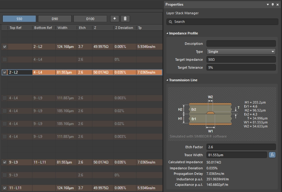
Calculation example (approximate): For a 50Ω trace on a 4-layer FR-4 board with 5-mil spacing to the ground plane, a trace width of roughly 6–8 mil is required. This varies with the copper thickness, the dielectric constant of the material, and the frequency.
Differential pairs: Two complementary signals routed close together with tight spacing control. Common in high-speed I/O like LVDS (Low Voltage Differential Signaling), USB 3.1, and RF differential signals. Differential impedance (the impedance between the two traces as a pair) is typically 85–110Ω (the industry standard is 100Ω for many high-speed standards).

Rule setup in CAD:
- Define “differential pair” rules specifying trace width tolerance (e.g., ±2 mil to maintain uniform impedance)
- Specify maximum spacing between the two traces (e.g., 8 mil)
- Specify length matching tolerance (e.g., ±10 mil) to keep propagation delay balanced
- Restrict which layers differential pairs can route on
Why this matters: A differential pair with unbalanced length or spacing will have impedance variation, causing common-mode noise, crosstalk, and potential signal integrity failures. This is especially critical in 5G RF circuits or DDR memory interfaces.
Return Path, Reference Plane, and Plane Splits
The return path for a signal is as important as the signal path itself. High-speed noise often comes from poor return paths.
Ground plane return: When a signal layer is adjacent to a ground plane, the return current flows directly underneath the signal in the ground plane, creating a tight loop with minimal inductance. This is ideal.
Plane split problem: If the ground plane is divided (split into separate regions for analog and digital), the return current cannot follow the signal. Instead, it must navigate around the split, creating a large loop area and generating EMI.
Common mistake: Designers split ground planes to separate “noisy” digital circuits from “sensitive” analog circuits. While the intent is good, the remedy often backfires. Modern best practice is to use a continuous, single ground plane and separate analog/digital through routing isolation and filtering, not plane splits.
Rule guideline: Avoid ground plane splits unless necessary. If they’re required (as in some isolated power applications), make sure all return paths can flow under the signal via other connected copper areas or vias.

Thermal, Power Integrity, and DFM-Oriented Design Rules
Thermal Relief, Copper Pours, and Heat Spreading
High-power components—processors, voltage regulators, MOSFETs—generate heat that must be dissipated, or the component fails thermally.
Copper pours are large regions of copper connected to power or ground nets. They improve current distribution and heat spreading.

Thermal relief is a pattern connecting a component pad or via to a large copper pour with narrow spokes instead of a solid connection. Why? During solder reflow, a solid connection to a large copper area acts as a heat sink, pulling heat away from the pad before solder melts. Thermal relief spokes limit heat loss, allowing proper solder wetting.
Thermal relief rules:
- Spoke width: typically 6–10 mil (wide enough to conduct current and heat, but narrow enough to provide thermal isolation during soldering)
- Number of spokes: typically 4 (one in each cardinal direction for vias, 2–3 for pads)
- Spoke length: just long enough to connect pad to the outer boundary of the copper pour
Copper pour management:
- Power pours should be thick (no minimum in EDA tools, but fabricated thicknesses are typically 1–3 oz copper per square foot)
- Ground pours should be continuous whenever possible
- For thermal management, pads and vias should be as large as possible to maximize thermal conductance to the surrounding copper
Rule example: “All vias connected to the 3.3V power pour must have 4 thermal relief spokes, each 8 mil wide.”
Power Delivery Network (PDN) Design Rules
A stable power supply voltage is critical for IC operation. PDN design rules ensure voltage doesn’t sag excessively under transient loads.
Key rules:
- Power distribution should use planes rather than thin traces. A power plane provides far more current capacity and lower impedance than a routed trace.
- Decoupling capacitors (bypass capacitors) should be placed as close as possible to the power pins of high-speed ICs. Distance = inductance = slower response time to voltage transients.
- Use capacitors of multiple values (e.g., 10µF, 1µF, 0.1µF, 0.01µF) in parallel to handle transients across a broad frequency range.
- For dense BGA packages, decoupling capacitors are often placed on the same layer as the BGA pads or on the opposite side of the board, directly under the BGA.
Design rule configuration:
- “All ICs operating at 3.3V must have a decoupling capacitor within 500 mil of the nearest VCC pin.”
- “High-speed processors must have a decoupling capacitor within 250 mil of each VCC pin.”
- “Return vias from capacitor pads must connect directly to the ground plane, not route through traces.”

DFM/DFA Rules From Your Manufacturer
Design for Manufacturability (DFM) and Design for Assembly (DFA) rules ensure your design can actually be built without errors, defects, or high cost.
Common DFM/DFA rules:
| Rule | Why It Matters |
|---|---|
| Min pad size for fine-pitch BGA | Pads that are too small cannot be reliably soldered; solder balls fail to wet properly. |
| Min solder mask bridge | Too narrow a bridge causes solder mask to bridge across, creating solder bridges between pins. |
| Min clearance for solder wave | Through-hole wave soldering equipment has nozzles that fit between component leads; clearance prevents collisions. |
| Test point size and spacing | Test points must be large enough (typically 50–75 mil) to accept probe tips; spacing prevents probe skipping. |
| Stencil aperture size (for stencil printing) | Solder paste is deposited through a steel stencil; aperture size controls paste volume. Too small and paste doesn’t come through; too large and solder bridges occur. |
| Via landing near pads | A via landing on a component pad can interfere with solder reflow; minimum clearance is typically 10–20 mil. |
Where to get these rules: Your assembly partner (the PCBA manufacturer) may have different requirements than your PCB fabricator. Always coordinate with both. IWDF Solutions, for instance, can provide a combined DFM/DFA rule set that accounts for both board-level capabilities and assembly requirements.
How to Set Up PCB Design Rules in Your CAD Tool (Beginner-Friendly Walkthrough)
Let’s assume you’re using Altium Designer or KiCad. The process is similar across tools.
Step 1: Gather Requirements
Before opening the design rule manager, compile:
- Your PCB manufacturer’s design rules (PDF or online specifications)
- Your assembly partner’s DFM/DFA constraints
- Industry standards relevant to your product (IPC-2221 for general design, IPC-6012 for rigid PCBs, IPC-A-600 for class requirements)
- Voltage/current specifications of your circuit
- Operating environment (consumer, industrial, automotive, medical)
Step 2: Define Net Classes
Most high-speed and specialized traces benefit from their own set of rules. In your CAD tool, create net classes:
- High-speed: DDR memory, PCIe, USB, HDMI
- Power: Main power rails (wider traces, larger vias)
- RF/Microwave: Controlled impedance signals
- Analog: Sensitive audio or measurement signals
- Digital: Standard logic signals
- GND: Ground net (special rules for ground vias and planes)
Step 3: Access the Design Rules Manager
In Altium Designer: Design → Rules
In KiCad: File → Board Setup → Design Rules
Step 4: Configure Trace and Space Rules
Under “Electrical” rules:
- Min Trace Width: Enter the manufacturer’s minimum (typically 3–4 mil). Set per net class if needed (power nets = wider).
- Trace Spacing: Enter the manufacturer’s minimum clearance (typically 3–4 mil).
- Width to Space Ratio: Some tools let you enforce a ratio rather than absolute minimums.
Example for Altium:
textRule Name: PowerTraces
Applies To: Net Class 'Power'
Min Width: 10 mil
Max Width: 100 mil
Step 5: Set Via Rules
Under “Electrical” → “Via Style”:
- Via Diameter: Set to the manufacturer’s standard (e.g., 12 mil)
- Min Hole Size: Manufacturer’s minimum drill size (e.g., 8 mil for standard, 4 mil for microvias)
- Annular Ring: Copper ring around the via hole (e.g., 3 mil minimum)
- Via Spacing: Minimum center-to-center distance between vias (typically 12–15 mil)
- Aspect Ratio: Maximum ratio of board thickness to hole diameter (typically 10:1)
Step 6: Configure Clearance Rules
Under “Physical” rules:
- Copper-to-Copper Clearance: Default clearance between all copper (e.g., 3 mil)
- Clearance to Board Edge: Minimum distance from copper to board outline (e.g., 40 mil)
- Silkscreen-to-Pad Clearance: Keep labels away from pads (e.g., 10 mil)
For high-voltage designs, add a separate clearance rule:
textRule Name: HighVoltageSpacing
Applies To: High-voltage nets (> 50V)
Clearance: 5 mil (or per IEC-60950 creepage table)
Step 7: Add High-Speed Rules (if applicable)
If your design includes controlled impedance:
- Go to “Electrical” → “Impedance.”
- Specify trace width and layer for each impedance target (50Ω, 75Ω, 100Ω differential, etc.)
- The tool can calculatethe required trace width based on the stackup and materials.
For differential pairs:
textRule Name: DifferentialPairs_USB3
Applies To: Differential pair nets
Max Coupled Length: 10 mil
Length Tolerance: ±10 mil
Characteristic Impedance: 100 Ω ±10%
Step 8: Run Design Rule Check (DRC)
Once rules are configured:
- Go to Tools → Design Rule Check (or similar in your CAD tool)
- Select all rules to check
- Run the check
- Review violations
Expected violations (if any) should be understood and justified. For example:
- A trace that doesn’t meet the minimum width due to routing constraints might be acceptable if it’s low-current
- A via close to a pad might be necessary for a BGA fanout
Step 9: Document Your Rules
Create a summary document or export the rules from your CAD tool. This becomes part of your design documentation and helps when collaborating with layout engineers or reviewers.

Common Mistakes When Setting PCB Design Rules (and How to Avoid Them)
Mistake 1: Using Default or Generic Rules
Many designers import default rules from their CAD tool template, which is often based on generic industry averages.
Problem: Default rules may be overly conservative (limiting your design density) or not matched to your specific manufacturer’s capabilities.
Solution: Always start with rules provided by your PCB fabricator and assembly partner. IWDF Solutions, for instance, will provide rules specifically tuned to their equipment and processes.
Mistake 2: Not Adjusting Rules for Different Signal Types
Using the same trace width for power rails and small signal traces is inefficient.
Problem: You waste space by making small signal traces too wide, or you create reliability issues by making power traces too narrow.
Solution: Define net classes and apply differentiated rules. High-current power rails should use the widest practical width. Sensitive analog signals might have tighter spacing to prevent crosstalk.
Mistake 3: Ignoring Creepage and Clearance in High-Voltage Designs
This is especially dangerous in industrial, automotive, or power supply designs.
Problem: High-voltage traces spaced too close can arc or degrade over time (especially in humid environments), leading to field failures and potential safety hazards.
Solution: Look up creepage/clearance requirements in IEC-60950, UL-61010, or other relevant standards. Create explicit rules for high-voltage nets.
Mistake 4: Treating All Layers the Same
Different layers have different characteristics. External layers experience different etching and copper plating than internal layers.
Problem: A trace width that works perfectly on an internal stripline layer might be too narrow on an external microstrip layer (different dielectric, no protective copper above).
Solution: Some manufacturers provide layer-specific design rules. Use them. In your CAD tool, you can define rules that apply only to certain layer types.
Mistake 5: Poor DFM Rule Configuration
Forgetting solder mask bridge rules, test point clearance, or panelization constraints leads to production holds.
Problem: Your PCB passes DRC in your software but fails the manufacturer’s pre-production review. Board has to be redesigned, delaying the project.
Solution: Request a complete DFM/DFA rule set from your manufacturing partner. Include rules for:
- Solder mask opening sizes and bridges
- Test point dimensions and spacing
- Panelization requirements (board edge clearance, panel tab style)
- Stencil aperture sizes (for paste printing)
Mistake 6: Not Accounting for Manufacturing Tolerances
Design rules should build in safety margins above the manufacturer’s minimum capability.
Problem: Designing right at the edge of process capability means small manufacturing variations can cause failures.
Solution: If your manufacturer’s minimum trace width is 3 mil, design with 4 mil minimum. If the minimum via diameter is 8 mil, use 10 mil for non-critical signals. Margins prevent yield loss and reliability issues.
When to Involve Your PCB Manufacturer in Design Rule Decisions
Early collaboration with your manufacturing partner is invaluable.
Pre-Schematic Phase
Before a single symbol is drawn, discuss with your board shop:
- Expected complexity (number of layers, density, special requirements)
- Target cost target and volume (prototype vs. low volume vs. mass production)
- Any unusual requirements (high-frequency, high-voltage, harsh environment, special materials)
Benefit: The manufacturer might suggest a stackup or layer count that reduces cost while meeting your goals.
During Schematic Review
Once the schematic is drawn but before layout:
- Share the schematic with your board shop and assembly partner
- Ask them to flag any manufacturability concerns (high pin-count BGA with tight fanout, many high-speed differential pairs, power delivery feasibility)
- Request preliminary design rule guidelines based on the schematic
Benefit: Catching manufacturability issues early is far cheaper than redesigning after layout.
During Layout Review (Pre-Gerber)
Before finalizing gerbers:
- Request a preliminary DFM review of your layout (many manufacturers offer this free or for a small fee)
- Share your stackup, high-frequency routing, and high-current paths for feedback
- Ask about their DFM software tool (many offer web-based tools like Sierra Circuits’ “Better DFM” or automated DFM checkers)
Benefit: Catching violations before you submit Gerbers prevents delays and respins.
FAQ: Short Answers About PCB Design Rules
Q1: What are the most critical PCB design rules for beginners?
A1: Trace width (for current capacity), trace spacing (to prevent shorts), via size (for reliability), and component clearance to board edge (for assembly safety). Start with these four, then expand to impedance and DFM rules as you advance.
Q2: What is the minimum trace width I should use for PCB design?
A2: It depends on the current and your manufacturer’s capability. For low-current signals, 3–4 mil is typical for standard PCBs. For power, calculate using IPC-2221 (roughly 1 amp per 15 mil width on outer layers with 10°C rise). Always verify with your manufacturer.
Q3: How do PCB design rules affect manufacturability and cost?
A3: Tighter design rules (narrower traces, tighter spacing) require more advanced manufacturing equipment and processes, increasing cost. Relaxed rules reduce cost but might limit circuit density. Proper rules balance cost and performance.
Q4: What design rules are critical for high-speed or RF PCBs?
A4: Controlled impedance (trace width/spacing), differential pair spacing and length matching, continuous ground planes, and return path management. High-speed noise is often caused by rule violations.
Q5: Should I use the default design rules in my PCB software?
A5: Only as a starting point. Default rules are usually generic and may not match your specific manufacturer’s capabilities or your design requirements. Always customize based on your board shop’s guidelines.
Q6: How do I know if my design follows the DFM (Design for Manufacturability) rules?
A6: Request a DFM review from your manufacturer before submitting final Gerbers. Many shops offer automated DFM checks (online tools) that catch common issues like insufficient solder mask bridges, test point conflicts, or panelization problems.
Q7: Can I design a PCB with just electrical rules, without worrying about manufacturing rules?
A7: Technically yes, but you’ll likely encounter production delays and rework. Manufacturing rules exist because they solve real-world production problems. Ignoring them is false economy.
Q8: How do impedance control rules work?
A8: Trace width and spacing to the reference plane (ground) are calculated to achieve a target impedance (usually 50Ω or 100Ω differential). Variations in width or spacing cause impedance variations, which cause signal reflections and integrity issues at high speeds.
Bringing Your Design to Life: How IWDF Solutions Supports Your PCB Design Journey
At IWDF Solutions, we understand that design rules are more than just technical constraints—they’re the foundation of product reliability and manufacturability. Whether you’re designing your first board or managing a portfolio of products across multiple industries, our team is here to ensure your design rules align with real-world manufacturing capabilities.
What We Provide
Free Design Rule Documentation: When you partner with IWDF Solutions, you receive:
- Complete design rule files for Altium Designer, KiCad, and other CAD tools
- Layer stackup recommendations based on your circuit’s signal integrity and power delivery requirements
- DFM/DFA guidelines tailored to our fabrication and assembly capabilities
- Standard rules for consumer, industrial, automotive, and medical applications
Pre-Production Design Review: Before your boards go into fabrication, we perform a thorough DFM/DFT review:
- Identify potential manufacturing or assembly issues early
- Suggest optimizations for cost, reliability, or performance
- Verify compliance with industry standards (IPC-2221, IPC-6012, relevant safety standards)
Manufacturing Rule Updates: As technology evolves and our equipment capabilities expand, we continuously update our design rules. New HDI capabilities, advanced materials, and higher-density processes are reflected in updated rule sets you can immediately adopt.
Design Consulting Support: For complex projects involving high-speed digital, RF, power delivery, or specialized requirements:
- Our engineering team reviews your design approach
- We suggest stackup architectures and material selections
- We validate signal integrity and EMI considerations
- We provide guidance on DFM trade-offs (density vs. cost, performance vs. manufacturability)
Why This Matters for Your Business
Risk Mitigation: Proper design rules prevent costly redesigns, production delays, and field failures. A design rule violation caught early costs a day or two of schedule. Caught in production, it costs weeks and thousands in rework.
Faster Time-to-Market: When your design follows manufacturer-validated rules, your boards pass DRC on the first submission. No respins, no delays.
Cost Optimization: Rules that are properly aligned to manufacturing capabilities allow you to:
- Achieve higher density without over-constraining the layout
- Use standard materials and stackups (lower cost) instead of custom solutions
- Avoid expensive “special process” flags
Long-Term Reliability: Rules validated against industry standards (IPC, IEC, UL) ensure your products perform reliably over their entire lifetime, even in harsh environments.
Getting Started
If you’re designing a new product or reviewing your current design rules, we’re here to help. Simply:
- Share your design objectives: Tell us about your circuit’s requirements (voltage, current, frequency, environment, volume).
- Provide your current PCB design or schematic: We’ll review manufacturability.
- Request design rule guidelines: We’ll provide files compatible with your CAD tool.
- Schedule a pre-production DFM review: Before you finalize your Gerbers, let us catch potential issues.
Contact IWDF Solutions today via our website or email info@iwdfsolutions.com. Our team responds within 24 hours and is committed to making your PCB design project a success—from concept through production.
Whether you need one-off prototypes or ongoing design support for a product family, IWDF Solutions is your partner in achieving reliable, cost-effective PCBs that meet global manufacturing and quality standards.