

Designing a PCB that looks good in CAD software doesn’t mean it can be manufactured without problems. Every year, some beginner engineers waste time and money fixing boards that failed simply because the design didn’t consider real-world manufacturing rules. That’s why understanding PCB design guidelines for DFM (Design for Manufacturability) is critical—even at the early layout stage.
PCB design guidelines for DFM include correct trace width, copper clearance, minimum drill sizes, proper component spacing, and avoiding dense via clusters. Following DFM rules ensures your board can be manufactured reliably, with fewer errors and delays. Both fabrication and assembly constraints must be considered early to prevent respins and yield issues.
Let’s go through these guidelines step-by-step to help you design PCBs that are not only functional but also production-ready.
What Is DFM in PCB Design and Why Does It Matter?
Design for Manufacturability (DFM) is the engineering practice of ensuring that a PCB layout can be fabricated, assembled, and tested with high yield, low cost, and minimal manual intervention. It’s not just about passing ERC and DRC checks—it’s about designing with the capabilities and limitations of real-world manufacturing processes in mind.
In the context of PCB design, DFM spans two primary domains:
- Fabrication DFM, which focuses on parameters like trace width and spacing, copper-to-edge clearance, drill tolerances, solder mask expansion, and board outline definitions.
- Assembly DFM, which addresses component placement, orientation, thermal reliefs, stencil apertures, and pick-and-place compatibility.
Designers often assume that if a board works electrically, it’s ready for manufacturing. But in practice, that’s rarely true. A board that ignores DFM rules can fail in subtle but expensive ways: poorly plated vias, solder bridging under dense QFNs, warped stack-ups, or stencils that can’t deposit solder properly.
Here’s why DFM matters at every stage of the product lifecycle:
- Reduces respins: A single fabrication mistake can delay a project by 2–3 weeks. Early DFM avoids these disruptions.
- Improves yield: Boards designed with proper spacing, pad geometry, and copper balancing are less likely to fail in production or burn-in tests.
- Lowers cost: Good DFM allows panel optimization, reduces manual rework, and prevents part scrapping due to placement issues or tombstoning.
Let’s look at a few typical issues that DFM can preempt:
| Problem | Cause | DFM Fix |
|---|---|---|
| Solder bridging | Pads or parts placed too close | Adjust pad spacing, refine stencil design |
| Open via near pad | Untented via under small components | Tent or move vias, especially near QFNs |
| Board warping | Asymmetric copper or poor stack-up | Use symmetric layer structure and plane fill |
| Trace breakage | Undersized or inconsistent width | Follow IPC-2221 width recommendations |
Tip: Treat DFM as an extension of your design phase, not an afterthought. Your PCB is only as good as its weakest manufacturing assumption.
What Are the Core DFM Rules in PCB Design?
DFM rules are not generic “best practices”—they’re factory-enforced physical constraints. Whether you’re designing a simple two-layer dev board or a dense six-layer embedded system, your design must conform to what your fabricator and assembler can reliably produce.
While each manufacturer publishes its design rule document, several parameters are considered baseline across most fabs. Let’s explore these core rules in detail—along with the reasoning behind them.
Minimum Trace Width and Spacing
The minimum trace width determines how much current a trace can carry, and whether it can be reliably etched. Most standard PCB fabs support ≥ 6 mil (0.152 mm) trace width and spacing, but if you’re routing high-density areas or high-speed signals, 4 mil rules may apply—with tighter fab tolerances and higher costs.
Smaller than 4 mil often requires laser direct imaging (LDI) processes or HDI stackups, which aren’t supported in all facilities.
Rule of thumb: Always confirm with your fab. And remember that internal layers often require more conservative spacing due to reduced etch-back precision.
Drill Size and Annular Ring
For through-hole vias, the drill size and surrounding annular ring must meet plating and alignment requirements.
- Standard mechanical drill: ≥ 0.3 mm
- Recommended annular ring: ≥ 0.15 mm (minimum), ≥ 0.25 mm (ideal for IPC Class 2+)
If the annular ring is too thin, drill wander (misregistration between drill and copper pad) can break connectivity. This is especially risky in stacked vias or when connecting power/ground planes.
When using tented vias under components, ensure there’s still enough ring to maintain reliable plating. If not, expect test failure or increased resistance.
Copper-to-Edge Clearance
Copper pours or traces must maintain enough distance from the board edge to avoid exposure during routing, V-scoring, or depaneling.
- Minimum clearance: ≥ 0.25 mm (standard); ≥ 0.5 mm for edge connectors or high-voltage regions.
Edge clearance issues commonly appear during panelization. If your copper is too close, you may get unexpected shorts or delamination at the edges.
If you’re using edge plating or castellated holes, coordinate with your fab early—these features require extra clearance and plating control.
Via Design
Blind and buried vias can reduce routing congestion, but they increase cost and introduce extra layers of process control. Unless you’re doing a complex HDI design or routing high-pin-count BGAs, stick with plated through-hole vias.
To avoid solder migration, tenting vias (covering them with soldermask) is essential under small packages. For via-in-pad configurations (e.g. under QFNs or BGAs), the via must be filled and capped—and the fab must be capable of planarizing the pad for proper stencil contact.
Avoid leaving untented vias near pads. Even if DRC passes, you’ll risk unpredictable solder behavior during reflow.
In summary, these are the minimum thresholds for a robust, DFM-compliant board. They’re not arbitrary—they reflect real equipment limitations, process tolerances, and assembly needs.
As a PCB designer, our job isn’t just to “route signals”—it’s to create something a factory can build repeatably and without special handling.
Why DFM Compliance Testing Is Essential Before Manufacturing?
Even if your design looks clean, it might still fail manufacturability checks. This is why DFM compliance testing is a critical step before sending files to fabrication.
What is DFM Compliance Testing?
It’s an automated check performed by your manufacturer or software to catch potential issues in your Gerber and drill files, such as:
- Trace-to-trace or trace-to-hole clearance violations
- Missing solder mask between pads
- Non-standard via-to-pad ratios
- Component spacing is too tight for assembly tools
How to Perform It
- Use tools like Altium Designer’s DRC + DFM checks, or free DFM checkers from your PCB vendor (e.g., Sierra Circuits, AdvancedPCB).
- Upload Gerber files to your vendor’s DFM portal before finalizing your BOM.
What Happens If You Skip This?
- Your board may fail in the factory and be sent back for redesign.
- Production delays from back-and-forth CAM feedback.
- Increased costs due to rush corrections or respins.
Tip: Make DFM testing part of your pre-production checklist. Don’t wait for fabrication to catch problems.
What Are the Most Important DFM Guidelines for PCB Layout?
Good PCB layout is not just about signal integrity—it’s also about manufacturability. Even if your board functions electrically, poor layout choices can make it hard or even impossible to fabricate.
Maintain Consistent Trace Widths
Use wider traces where possible—especially for power and ground paths. Avoid sudden width changes, which can create acid traps during etching or weak spots for high current.
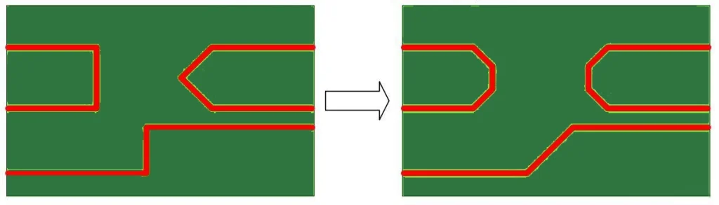
Avoid Acute Angles
Keep trace corners at 45° angles, not sharp 90°. Acute angles can trap etchant and lead to over-etching or open circuits.
Minimize Copper Islands
Floating or isolated copper areas can peel during reflow or create unwanted capacitance. Always tie islands to a net or remove them entirely.
Keep Return Paths Clear
Ensure ground planes are continuous beneath signal traces, especially high-speed lines. Broken return paths can generate EMI and cause signal integrity issues.
Use Grid-Based Placement
Align traces and vias to a fixed grid (e.g., 0.1 mm). This helps auto-routing tools and reduces the chance of non-standard spacing errors.
Tip: Always run a layout-specific DFM review before you finalize the file set. Software DRC is not enough—it doesn’t account for real-world fab processes.
How Component Placement Affects PCB Manufacturability?
Component placement is one of the most overlooked DFM elements—especially by beginners. But it’s also one of the most impactful. Poor placement leads to soldering issues, inspection difficulty, and pick-and-place machine errors.
Start with Connectors and Critical ICs
- Place connectors along the board edge.
- Keep USB, HDMI, or power jacks on the same side.
- Align high-speed components near their corresponding interface chips.
Respect Minimum Component Spacing
- Leave at least 0.5 mm clearance between components.
- For large parts (e.g., capacitors, connectors), increase spacing to allow for machine nozzle access.
Group Similar Components
- Keep resistors and capacitors aligned and grouped by function.
- This helps with inspection, rework and reduces pick-and-place programming errors.
Avoid Placing Components Near Board Edges
Vibration during panel separation can crack solder joints. Keep delicate components like crystals and small capacitors at least 2 mm away from board edges.
Follow Orientation Consistency
Orient polarized components (like diodes or ICs) the same way across the board. It reduces assembly errors and speeds up visual inspection.
Tip: Ask your assembler for their placement guidelines. Many provide a “PCB Assembly DFM checklist”—follow it from the start.
What Should Be on Your PCB DFM Checklist?
A practical DFM checklist helps ensure your design won’t hit surprises during manufacturing. Whether you’re working with a contract manufacturer or sending to a prototype house, you should always run through this checklist before generating Gerber.
PCB Fabrication Checklist
- Minimum trace width and spacing respected (per manufacturer specs)
- Drill sizes ≥ 0.3 mm, with matching annular rings
- Proper copper-to-edge clearance (≥ 0.25 mm)
- No overlapping or unnecessary vias-in-pad
- Clean silkscreen (no text over pads or vias)
- Solder mask openings are properly aligned with pads
- The board outline is clearly defined in its layer

PCB Assembly Checklist
- Components follow standard spacing rules (≥ 0.5 mm where possible)
- Polarized parts are consistently oriented
- No components placed near mounting holes or board edges
- Pads sized for stencil printing (per IPC-7351)
- Avoided tombstoning risks (e.g., with unequal thermal pads)
- Component reference designators are readable after assembly
Tip: Use this checklist together with your manufacturer’s official DFM checklist—they often provide it in PDF or online form. Search for “PCB DFM checklist PDF” from trusted vendors like Sierra Circuits or AdvancedPCB.
Summary: Design for Manufacturability Is Design for Success
Designing a great PCB is not just about getting the circuit right—it’s about making sure it can be built, tested, and assembled without friction. Following DFM guidelines helps reduce production delays, avoid respins, and increase product quality. Make DFM part of your design workflow—not an afterthought.
Still unsure if your design is ready for fabrication? Contact a one-stop design-to-manufacture partner to review your layout before sending files out.