
You need a replacement board. The OEM is gone. The design files never existed. Every day the machine is down, the pressure builds. The wrong service choice here means weeks of avoidable delay.
PCB reverse engineering disassembles an existing board to understand its structure and function — producing schematics, Gerber files, and a BOM, while enabling component upgrades and design improvements. PCB cloning reproduces the design of an existing board to deliver a functionally identical replacement. They are two distinct processes, and knowing which one your project actually needs is the decision that determines whether things move fast or stall.
Most buyers arrive at this topic with a single goal: get a working board back in service. What they often discover is that they’re actually asking two separate questions at once — “Can someone figure out what’s on this board?” and “Can someone make me more of them?” These are different problems. They require different skills and different timelines. But they do not require different vendors. A factory with genuine PCB reverse engineering capability already has everything needed to take that project all the way through to finished, tested boards. The real decision is whether you need both phases — or just one. Getting that answer right is what keeps your project on schedule instead of being stalled.
What Is the Difference Between PCB Reverse Engineering and PCB Cloning?
You’ve seen both terms on supplier websites. You’ve probably assumed they mean roughly the same thing. They don’t — and that gap in understanding usually shows up as miscommunication: the wrong scope gets quoted, expectations don’t match, and what should have been a straightforward project takes longer than it needed to.
PCB cloning copies the design of an existing board to reproduce its function exactly. PCB reverse engineering goes further — it disassembles the board layer by layer to understand how it works, then uses that understanding to restore it, improve it, and produce engineering files that give you permanent ownership of the design.
PCB Cloning: What It Actually Means
PCB cloning reproduces the design of an existing circuit board to achieve the same function. The goal is a working board that behaves the same way as the original — component for component, connection for connection. Nothing about the design is analyzed or fundamentally changed. The board is reproduced as it was.
This makes cloning the right service when you know exactly what you want and you want it replicated faithfully. It is fast and direct. But it works best when the original design is already sound — when the components are still available, when the board meets current regulatory standards, and when no improvements are needed. If any of those conditions do not hold, cloning alone is not enough.
PCB Reverse Engineering: What It Actually Means
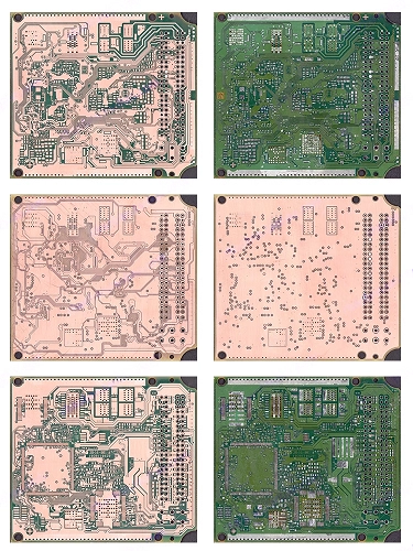
PCB reverse engineering goes further than cloning. It involves physically disassembling an existing PCB — layer by layer — to understand its structure and how it works. Engineers trace every copper connection, identify every component, and map how the circuit functions as a whole. That process produces a complete set of engineering files: Gerber files, a schematic diagram, a Bill of Materials, and pick-and-place data.
But the output is not just documentation. That understanding becomes the basis for something more useful than simple reproduction. It allows engineers to study the design, identify weaknesses, replace discontinued components with modern equivalents, improve circuit efficiency, and bring the board in line with current regulations and manufacturing standards.
This is exactly why PCB reverse engineering is just as much about improvement as it is about repair. Think about a board designed 15 years ago—chances are, many of its components are now end-of-life, lag behind today’s efficiency standards, or fail to meet modern RoHS regulations. Reverse engineering gives engineers the visibility they need to not just clone the original design, but to actually refine and optimize it for the modern market.
Both processes are essential for real-world challenges — an obsolete control board with no OEM support, a complex system that has failed without any documentation, or a design that needs to be brought forward to current manufacturing standards. Neither is always sufficient on its own. Together, they cover the full range of what professional PCB recovery and reproduction requires.

How the Two Processes Relate
| PCB Reverse Engineering | PCB Clone | |
|---|---|---|
| Input | Physical PCB sample | RE files or existing design files |
| Output | Gerber, BOM, Schematic, PnP files + restored/improved board | Fabricated, assembled, tested boards |
| Primary purpose | Design analysis, documentation, IP recovery, improvement | Faithful reproduction of existing design |
| Includes design analysis? | Yes | No |
| Supports component substitution? | Yes — obsolete parts replaced with modern equivalents | Only if RE phase is included |
| Supports design improvement? | Yes | Only if RE phase is included |
| Includes manufacturing? | Yes — leads to finished boards | Yes |
| Typical timeline (2-layer) | 3–5 days for files; full boards within standard production lead time | Faster if files already exist |
| Requires IC unlock? | Sometimes — if board has encrypted MCUs | Same |
| Who retains IP? | Client owns all derived files and hardware | Client owns hardware |
The clearest way to state the relationship: PCB reverse engineering is the upstream analytical and engineering phase. PCB cloning is the downstream manufacturing execution. You can commission cloning without reverse engineering — but only if you already have verified design files. If you are starting from a physical board with no files, reverse engineering comes first.
Is PCB Reverse Engineering Really Just “Copying” a Board?
This is the question that trips up buyers working through this for the first time. The assumption is reasonable — you hand over a board, you get back a board. But the process in between is not copying. And that distinction matters both technically and legally.
A properly reverse-engineered PCB is not a photocopy of the original. It is a reconstructed set of engineering files that reproduce the original board’s electrical behavior — while giving engineers the opportunity to update components, correct inefficiencies, and ensure compliance with current standards.
Why the Output Will Differ From the Original?
When an engineer reverse engineers a multilayer board, the process is reconstruction, not scanning. The engineer reads the circuit from the physical board, identifies every component and its electrical function, and redraws the layout from that schematic — applying engineering judgment to route traces correctly and efficiently.
Three things will typically differ in the resulting files:
Component substitution. Boards designed five or ten years ago contain components that are now obsolete, restricted under RoHS or REACH, or simply unavailable. A professional BOM identifies these and provides modern equivalents with identical or superior specifications. This is not a compromise — it is what makes the board manufacturable today, using components that are actually in current supply.
Trace geometry. Because the engineer routes the board from schematic logic rather than tracing physical copper directly, the trace paths in the new Gerber files may differ from the original. The electrical connections are identical. The exact routing path of an inner layer trace does not need to match the original to produce a functionally equivalent board.
Layer stack reconstruction for multilayer boards. For 6-layer boards and above, inner layer trace geometry cannot be determined from surface inspection alone. Layer-by-layer delayering or X-ray CT imaging is required to capture buried and blind via structures accurately. The result is an independently constructed inner layer layout — not a reproduction of the original artwork.
Why This Also Has Legal Significance?
Under U.S. copyright law, a PCB layout reconstructed independently through schematic analysis is not considered a copy of the original layout. Copyright on a circuit board layout covers the specific artistic expression of the traces — not the underlying functional circuit. This is why professional PCB reverse engineering services can operate legally for repair, maintenance, and interoperability purposes. The output is a newly constructed work, not a reproduction.
The practical boundary: professional reverse engineering conducted through independent engineering reconstruction has legal standing in most jurisdictions. Photographic layer-by-layer copying without engineering reconstruction does not. A reputable provider operates on the right side of that line — and can explain exactly why.
When Should You Choose PCB Reverse Engineering?
Not every project ends with a purchase order for new boards. There are situations where the engineering files are the entire deliverable — and manufacturing is either handled in-house, deferred, or not needed at all.
If your goal is design recovery, analysis, compliance documentation, or using an existing board as a starting point for improvement — a PCB reverse engineering engagement gives you the files and the understanding you need, with or without a follow-on production run.
Scenario 1: Your Design Files Were Lost or Never Created
This is the most common reason companies come to us. The original board was designed by a contractor who is no longer available. The files were on a server that was never backed up. The OEM designed the board and retained the files. The board has been in service for years, but nobody on the current team has the design data.
Without Gerber files and a schematic, you cannot modify the board, qualify a second manufacturer, or make a compliant change for regulatory resubmission. Reverse engineering gives you back control of your own product — not just a copy of the board, but transferable intellectual property that you own going forward.
Scenario 2: Components Are Obsolete or Non-Compliant
When a board’s original BOM contains discontinued parts, lead-containing components, or materials restricted under current environmental regulations, you cannot simply reproduce the board as-is. Reverse engineering creates the opportunity to identify every affected component and qualify a modern equivalent before any production begins. The result is a board that is both functionally identical to the original and buildable with today’s supply chain.
Scenario 3: Competitive Design Analysis and Benchmarking
Engineering teams in mature industries — industrial controls, consumer electronics, telecommunications — regularly reverse engineer commercially available products for competitive analysis. Understanding a competitor’s component selection, layer count strategy, thermal management approach, and power architecture is legitimate engineering intelligence. It informs your own R&D decisions without copying anything for commercial use.
Scenario 4: Failure Analysis
A board fails in the field. No design documentation exists. The failure mode is unclear. Reverse engineering the failed board — and comparing it at the schematic level against a known-good sample — gives engineers the visibility needed to identify whether the failure is a design defect, a manufacturing defect, or a component quality issue. This is particularly critical in regulated industries where a documented root cause analysis is a regulatory requirement.
Scenario 5: Design Improvement Before Replication
Some clients do not want an exact reproduction. They want a modernized version — smaller form factor, reduced power consumption, added connectivity, updated certifications. Reverse engineering provides the functional baseline. The engineering team modifies the files before any fabrication begins. The production board is based on the original design but improved. This is not cloning. It is using reverse engineering as the foundation for new design work.
When Does a Full PCB Clone Service Make More Sense?
Reverse engineering solves the documentation and understanding problem. But in most operational situations, the problem is hardware. You need boards that work.
A full PCB clone service — covering everything from sample receipt through reverse engineering, fabrication, assembly, and testing — is the right choice when you need functional replacement boards and want a single accountable partner managing the entire process.
The Core Use Cases for Full-Service PCB Cloning
Legacy equipment maintenance. Industrial facilities, utilities, and infrastructure operators run equipment with lifecycles of 15 to 30 years. When a control board fails and the OEM no longer supports it, a clone is often the only alternative to replacing an entire system that cost six figures. A single production line shutdown caused by one obsolete PCB can cost more in lost output than the entire clone project.
This is the situation we see most frequently: CNC machine controllers, PLC interface boards, servo drive control cards, industrial power supply modules, and HVAC control boards. The equipment itself is mechanically sound. The PCB is the only failure point. A clone restores it to full service without a capital equipment replacement.
OEM discontinuation. When a manufacturer discontinues a product line and provides no upgrade path, buyers are left with equipment that has no official support. Finding remaining new-old-stock inventory is finite and increasingly expensive. A clone project creates a reliable supply of tested boards that can be stocked and used over years.
Supply chain disruption. Component shortages have become a structural challenge in electronics manufacturing. When a board’s original BOM is affected by unavailability, a reverse engineering phase that identifies and qualifies alternative components — followed by a production run of the modified board — solves the supply chain problem without requiring a full redesign from scratch.
Lost design files with immediate production need. If your design files are gone and you also need boards now, you need both phases. The standalone reverse engineering use case applies when time allows for a measured approach. The full clone service applies when you need hardware and cannot wait.
| Situation | What You Need | Recommended Service |
|---|---|---|
| Lost design files, no immediate production need | Engineering files only | PCB Reverse Engineering only |
| Lost design files, need boards urgently | Files + hardware | Full PCB Clone Service |
| OEM-discontinued board, need replacements | Files + hardware | Full PCB Clone Service |
| Obsolete or RoHS non-compliant components | Updated BOM + new boards | PCB RE + Design Update + Production |
| Competitive analysis / IP documentation | Engineering report | PCB Reverse Engineering only |
| Board redesign or modernization | Files as starting point | RE + PCB Design Service |
| Failure analysis | Schematic for root cause comparison | PCB Reverse Engineering only |
| Spare board inventory build | Files + hardware | Full PCB Clone Service |
What Should a Legitimate PCB Reverse Engineering Service Actually Deliver?
There is a wide gap between providers who claim to offer PCB reverse engineering and those who do it properly. Knowing what a professional deliverable looks like protects you from paying for work that cannot be used.
A professional PCB reverse engineering engagement delivers a complete, independently verified set of manufacturing-ready files — not scanned images, not incomplete schematics, and not Gerber files that require additional engineering work before they can be fabricated.
The Full Deliverable Set
Every reverse engineering project should produce the following, regardless of board complexity:
Gerber files in RS-274X format — one file per layer (copper, solder mask, silkscreen, board outline), plus mechanical drill files and laser drill files for blind and buried vias. These must be directly readable by any modern PCB fabrication system without conversion.
Fully annotated schematic diagram — not a block diagram, not a simplified overview. A complete schematic with every component represented, every net named, and reference designators consistent with the BOM. This is the document that allows anyone to understand how the circuit works.
Complete BOM with sourcing alternatives — every component listed with manufacturer, part number, description, package, value, quantity per board, and at least one alternative for any component that is obsolete or at supply risk.
Pick-and-place / centroid data — component X/Y coordinates, rotation, and board side for every SMT component. Without this file, every component must be placed manually — which dramatically increases both assembly cost and error risk.
Layer Capability and What It Signals About a Provider
| Board Type | Inner-Layer Method | Typical File Delivery |
|---|---|---|
| 1–2 layer | Optical inspection | 3–5 business days |
| 4–6 layer | Optical + controlled delayering | 7–12 business days |
| 8–12 layer | X-ray CT + delayering | 12–15 business days |
| 14–32 layer | X-ray CT + sequential delayering | 15–20+ business days |
| Rigid-flex / HDI | Specialized materials analysis | Project-dependent |
Any provider who quotes identical turnaround times for a 2-layer board and a 10-layer board is not doing the inner-layer work properly. Layer count and imaging method are the first technical questions to ask before committing to a project.
Verification: The Step That Separates Good Work From Acceptable Work
File delivery is not the end of a professional project. The delivered files should be verified by producing a bare board prototype and confirming dimensional accuracy and electrical continuity against the original sample. Ask your provider explicitly: “How do you verify the accuracy of the files before you deliver them?” A clear, specific answer is a professional signal. A vague or evasive answer is not.
Which Industries Actually Rely on These Services?
PCB reverse engineering and PCB cloning are active, recurring requirements across most industries that depend on electronic hardware. The common thread is the same across all of them: hardware lifecycles that exceed the support periods of the original designers, combined with real operational pressure to maintain equipment that cannot be easily replaced.
Every industry on this list has the same underlying problem — equipment built to last decades, running on boards that were designed once and never documented for the long term.
Industrial Automation and Manufacturing
Factory equipment is built to run for 20 years or more. The PCBs inside controllers, drives, and sensors are often tied to a generation of components that has since been discontinued. When a board fails, the machine stops. Reverse engineering and cloning restore the machine to service without triggering a capital replacement cycle.
The boards most commonly involved: PLC interface cards, CNC axis controller boards, servo drive control modules, HMI interface cards, and industrial power supply boards.
Aerospace and Defense
Systems deployed in aircraft, satellites, and defense platforms must remain functional for decades. Original suppliers may have closed. Manufacturing processes may no longer meet current standards. PCB reverse engineering enables documentation updates for continuing airworthiness, and cloning produces certified-quality replacement hardware. Every deliverable in this sector must be fully traceable — which makes the quality of the reverse engineering output especially critical.
Automotive
Discontinued ECUs, body control modules, ABS control boards, and sensor interface cards are regularly cloned for vehicle maintenance and fleet servicing. Rigid-flex PCBs, which are increasingly common in modern vehicles, require providers with specific materials knowledge beyond standard rigid board capability.
Medical Devices
A failed PCB in a ventilator, imaging system, or infusion pump carries consequences that go beyond equipment downtime. Medical facilities and biomedical engineering teams depend on PCB cloning to maintain life-critical equipment when OEM support ends — often long before the equipment is clinically retired. Providers in this sector must meet significantly stricter quality and documentation standards, including traceability requirements that do not apply in general industrial work.
Telecommunications and Energy Infrastructure
Legacy switching hardware, base station boards, and grid monitoring equipment continue to operate in networks built on infrastructure that predates current manufacturing norms. Reverse engineering ensures maintenance teams have the documentation they need. Cloning ensures failed boards can be replaced without system downtime.
How Do You Actually Choose a PCB Reverse Engineering Partner in China?
Shenzhen and the wider Guangdong Province represent the world’s densest concentration of PCB manufacturing and reverse engineering capability. The infrastructure — precision equipment, experienced engineers, component distributors within driving distance — creates capabilities and turnaround speeds that are genuinely difficult to match elsewhere. But the range of quality is equally wide.
Choosing the wrong provider means paying for files you cannot use, boards that fail functional testing, or — in the worst case — losing your only physical sample with nothing to show for it.
The Questions That Separate Professional Providers From Low-Cost Operators
What layer count can you handle, and what method do you use for inner layers?
A credible answer is specific: “We handle up to 32 layers using X-ray CT and sequential chemical delayering.” A non-answer — “We can handle any board” — tells you nothing useful.
What file formats will you deliver, and how do you verify accuracy?
The answer should include: Gerber RS-274X, fully annotated schematic, complete BOM with cross-references, and pick-and-place data — confirmed by a bare board prototype verification against the original sample.
Do you handle IC unlock in-house?
If your board contains microcontrollers or FPGAs with embedded firmware, the clone will not function without that firmware. Ask whether IC unlock is handled in-house or subcontracted, and whether the provider can assess feasibility for your specific IC models before you commit.
Are you a direct manufacturer or an intermediary?
Some companies present as manufacturers but send both the engineering work and the fabrication to third parties. This creates accountability gaps at exactly the moments when problems need to be resolved quickly. Ask for facility photos, request a video call, and confirm where the work is physically performed.
What certifications does your quality system carry?
ISO 9001 is the baseline for any serious provider. For regulated industry clients, look for ISO 13485 for medical devices or AS9100 for aerospace. Request the actual certificate numbers and verify them independently before sending your sample.
Red Flags Worth Knowing Before You Start
| Warning Sign | What It Likely Means |
|---|---|
| Quote provided without asking about layer count or IC list | Quoting a generic service, not your specific board |
| Identical turnaround for 2-layer and 8-layer boards | Inner layers are not being properly captured |
| Files delivered as PDF or image formats only | Not manufacturing-ready Gerber files |
| No verification step mentioned in scope | Files are not tested against the original sample |
| Unable to describe their equipment or process | Likely an intermediary, not a manufacturer |
| No clear policy on sample handling and return | Risk of losing your only physical reference |
What Are the Legal Boundaries You Need to Understand Before You Start?
Legal permissibility is a real question for B2B buyers — and it is worth addressing before commissioning a project, not after something has gone wrong.
PCB reverse engineering for maintenance, repair, interoperability, or internal analysis is broadly legal in the US, EU, and most of Asia-Pacific. Producing counterfeit versions of branded products is not. The line between the two depends on intent, method, and what you do with the output.
What the Law Actually Says
In the United States, a PCB layout reconstructed independently through schematic analysis is not a copyright-infringing copy of the original. Copyright on a circuit board layout covers the specific artistic expression of the traces — not the underlying functional circuit design. The Semiconductor Chip Protection Act explicitly permits reverse engineering for analysis and research purposes.
The EU similarly permits reverse engineering for purposes of research, interoperability, and independent study under applicable software and semiconductor directives.
The Practical Boundaries
Permitted in most jurisdictions:
- Reverse engineering a board you own for maintenance and repair
- Producing a functionally equivalent board through independent engineering reconstruction
- Reverse engineering a product for competitive analysis for internal use
- IP documentation and patent analysis for legal proceedings
Not permitted:
- Photographically reproducing copper layouts without independent engineering reconstruction
- Producing boards for sale that are marketed as the original manufacturer’s product
- Reproducing designs covered by active, enforceable patents without authorization
IC Unlock: A Separate Legal Consideration
If your board contains microcontrollers or programmable ICs with encrypted firmware, reproducing a functional clone requires unlocking and duplicating that firmware. This is technically possible for many common MCU families. Whether it is legally permissible depends on the specific component, who owns the rights to the embedded software, and the intended use.

At IWDF Solutions, we require clients to confirm that their intended use of reverse engineering output is lawful in their jurisdiction. The engineering work is our responsibility. IP compliance is the client’s responsibility — and a reputable provider will be transparent about this rather than pretending the legal dimension does not exist.
Frequently Asked Questions
Q: Can I commission PCB reverse engineering without sending my physical board to China?
No — not if you want professional results. Physical access to the board is required for component identification, layer imaging, and verification against the original. We accept international shipments with full customs documentation support, and the original sample is returned after project completion unless destructive delayering is required — which we always disclose before starting.
Q: How do I know the Gerber files delivered are actually accurate?
Ask explicitly for a verification protocol. A professional provider produces a bare board prototype from the delivered files and confirms dimensional accuracy and electrical continuity against your original sample before final delivery. If a provider cannot clearly explain their verification process, the files are unverified. This is the single most important due-diligence question you can ask.
Q: What happens when some components on my board are obsolete or discontinued?
A complete BOM flags obsolete components and provides modern equivalents with identical or superior specifications. For most standard passives and logic ICs, direct drop-in equivalents are available. For specialized or proprietary ICs, the engineer will assess the functional implications and recommend the appropriate path — direct equivalent, functional substitute with minor circuit modification, or redesign of that section.
Q: Can you clone a board that has blind vias and buried vias?
Yes. Boards with blind vias, buried vias, and via-in-pad structures require X-ray CT imaging or sequential chemical delayering to capture inner layer geometry accurately. This is standard capability for providers equipped to handle 6-layer and above boards. Confirm layer count capability and inner-layer imaging method before you commit to a provider.
Q: What is the realistic total timeline from sending my sample to receiving finished boards?
For a standard two-layer board: engineering files in 3–5 business days, PCB fabrication and assembly adding standard production lead time of 5–10 days for prototype quantities. Total elapsed time: 3–4 weeks for simple boards. For multilayer or BGA-heavy boards: 5–7 weeks. For projects requiring IC unlock: add 1–2 weeks for that phase. These timelines assume clean sample quality and prompt client response on component alternatives.
Q: Should I sign an NDA before the project starts?
Yes — always. Any reputable provider will offer a mutual NDA as standard practice. Request one even if it is not offered. The NDA should cover the confidentiality of your board design, your company identity, and all project files — and should explicitly state that no files derived from your project will be reused, shared, or retained beyond project completion.
Q: What is the difference between PCB reverse engineering and PCB copy — are they the same?
“PCB copy” is informal language often used for the same process. The meaningful distinction is not in the terminology — it is in the methodology. Professional reverse engineering reconstructs files through independent engineering analysis. Low-quality copying reproduces layouts photographically without engineering verification. The output quality differs significantly. When evaluating providers, ask about their methodology and verification process, not just what they call the service.
Q: Can IWDF Solutions handle both the reverse engineering and the full PCBA production?
Yes. IWDF Solutions operates as a fully integrated one-stop service provider. We reverse engineer the board, deliver the complete file package, fabricate the PCB — rigid, flex, or rigid-flex — source components, assemble via SMT and DIP processes, and perform AOI and functional testing, all under a single project and single point of contact. Clients who have preferred manufacturing partners elsewhere can commission the engineering deliverables only.
IWDF Solutions provides PCB reverse engineering services, PCB clone services, PCB design, and full-turnkey PCBA manufacturing from Shenzhen, China. Contact our engineering team to discuss your project and receive a technical assessment before committing to a scope.

