

PCB reverse engineering for mechanical and industrial equipment is about keeping critical machines running when their control boards are obsolete, undocumented or no longer supported. It gives you a practical way to repair, redesign or reproduce key PCBs so you can avoid costly downtime and full equipment replacement.
What Is Mechanical Parts PCB Reverse Engineering?
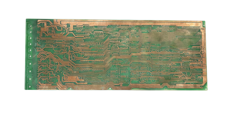
Mechanical parts PCB reverse engineering is the process of analyzing an existing circuit board used in mechanical or industrial equipment to rebuild its schematics, PCB layout and bill of materials so the board can be repaired, redesigned, or re‑manufactured when original documentation or support is no longer available.
In practice, this usually means:
- Taking a physical control or driver board from a mechanical machine and documenting its circuits and components in detail.
- Recreating the schematic, PCB layout and BOM in CAD tools so the board can be produced again or improved.
- Solving problems like discontinued parts, undocumented modifications and unknown design intent in older equipment.
- Preparing the reverse‑engineered board for small‑batch or volume production and long‑term support.
This is especially valuable in industrial automation, construction machinery, CNC machines, robotics and other mechanical systems where a single failed PCB can stop an entire line or machine.

Who Needs Mechanical Parts PCB Reverse Engineering?
Mechanical parts’ PCB reverse engineering is not just for electronics specialists; it is often driven by maintenance, operations and project teams who cannot afford long downtime. Industrial automation environments, construction sites and factories often rely on legacy PCBs that have long outlived their original design life.
Typical groups who benefit:
- Industrial equipment OEMs and mechanical machinery manufacturers need to support older models after the original design files are lost or incomplete.
- Plant maintenance (MRO) and reliability engineers are responsible for keeping production lines and heavy equipment running despite obsolete control boards.
- System integrators and retrofit companies are upgrading controls or adding new features to existing mechanical systems.
- Procurement and supply chain managers looking for a reliable PCB reverse engineering and manufacturing partner in China for industrial boards.
Their real‑world problems often look like this:
- A CNC machine or robot controller fails, and the OEM no longer sells spare boards.
- A PLC I/O card or motor drive board is discontinued, but there are still hundreds of machines in service.
- Documentation is incomplete or missing, making troubleshooting and upgrades slow and risky.
Applications of PCB Reverse Engineering in Mechanical and Industrial Systems
In mechanical and industrial environments, reverse-engineered PCBs are almost always tied directly to large physical assets. These boards must survive harsh conditions, including constant vibration, extreme temperature fluctuations, industrial dust, and 24/7 operating cycles.
Common Applications Include:
- Motion & Motor Control Systems: High-performance motor controllers, servo driver boards, and stepper drivers used in CNC machines, multi-axis industrial robots, and automated conveyor systems.
- Power Conversion & Management: Industrial inverters, power modules, and high-density power supply units (PSUs). These are critical for managing energy flow in renewable energy setups, heavy-duty machinery, and backup power systems.
- Custom Control & Development Boards: Proprietary development control boards and embedded logic units that manage specific industrial processes or specialized mechanical workflows where off-the-shelf solutions don’t exist.
- Power Switching & Distribution: Power switches, heavy-duty relays, and soft-starter PCBs that manage the initial high-current draw of pumps, compressors, and large-scale mechanical equipment.
- Automation & Interface Logic: PLC I/O boards and communication interface boards that bridge sensors, actuators, and field buses (like Modbus or CAN bus) across a production line.
- Sense & Safety Systems: Sensor interface boards for encoders and pressure sensors, along with safety and interlock boards that supervise emergency stops and door switches to ensure operator protection.
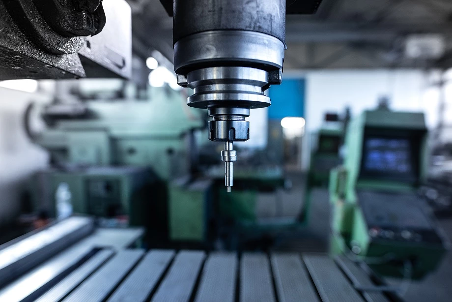
A Typical Scenario: A factory running a 20-year-old press line experiences a failure in a proprietary IGBT power module or a specific motor controller. Because the original manufacturer (OEM) is no longer in business and the technical documentation has long been lost, the board is effectively irreplaceable.
By applying PCB reverse engineering, the factory can:
Build a strategic stock of spares, eliminating the risk of future downtime without needing to replace the entire machine.
Analyze and replicate the obsolete board’s schematic and Gerber files.
Produce compatible replacements using modern, more reliable components.
Extend the lifespan of the entire multi-million dollar press line.
Mechanical Parts PCB Reverse Engineering vs Standard PCB Reverse Engineering
Reverse engineering an industrial control board inside a mechanical system is different from copying a consumer electronics PCB. The environment, risk and objectives are not the same.
Key differences at a glance
| Aspect | Standard PCB Reverse Engineering | Mechanical Parts PCB Reverse Engineering |
|---|---|---|
| Application | Consumer devices, general electronics like gadgets and small instruments. | High vibration, dust, oil, temperature swings, and long duty cycles. |
| Environment | Mild, shorter life cycles, limited vibration and dust. | Legacy components, high voltages, safety functions, mechanical constraints, and certifications. |
| Main Challenges | Fine‑pitch ICs, dense layouts, aesthetic constraints. | Legacy components, high voltages, safety functions, mechanical constraints and certifications. |
| Typical Goal | Clone or redesign a PCB for repair or small‑scale reproduction. | Keep expensive assets running, solve obsolescence, improve robustness while staying mechanically compatible.< |
| Risk Impact | A failed board affects a device or user experience. | A failed board can stop a line, idle a crane or affect operator safety. |
Because of these differences, mechanical parts PCB reverse engineering pays more attention to compatibility with existing enclosures, connectors, voltages, safety behavior and long‑term maintainability than a typical consumer PCB copy would.

Step‑by‑Step Process of Mechanical Parts PCB Reverse Engineering
Step 1 – Project Scoping and Legal Check
Every PCB reverse engineering project should begin with a clear scope and a basic legal review. This helps you avoid misunderstandings, wasted work and legal risk later.
Key questions to clarify early:
- What is the goal: repair a single machine, build spares, redesign with new components or upgrade functionality?
- Who owns the machine and PCB, and do they have the right to authorize reverse engineering work?
- Are there known patents, copyrights or contractual restrictions related to the board or system?
For most industrial users, the practical rule of thumb is that reverse engineering should be tied to equipment you legitimately own or maintain and should respect local intellectual property laws. For sensitive cases or projects in regulated industries, it is advisable to consult your legal team for an opinion before undertaking a large-scale reverse engineering effort.
From a practical standpoint, you should gather at least:
- Clear photos of the board in the machine, showing how it mounts and connects.
- Any existing drawings, wiring diagrams, manuals or part numbers.
- A description of the failure mode and whether other boards of the same type are still working.
Step 2 – Initial PCB Board Inspection and Documentation
Once a sample board is available, the first technical step is a thorough visual inspection, measurement and photo documentation. This is your “snapshot” of the original design before you touch anything.
Typical actions:
- Inspect physical condition: burnt areas, cracked solder joints, corrosion, melted connectors or damaged traces.
- Measure and record the board outline, mounting hole positions, connector locations and keep‑out zones relative to the mechanical enclosure.
- Capture high‑resolution photos of both sides with a ruler for scale, and if needed, use a flatbed scanner to record silk, pads and routing.
For mechanical systems, it is particularly important to note:
- Heavy components such as transformers, relays, heat sinks and large connectors that affect weight and vibration behavior.
- High‑voltage creepage distances and isolation slots between primary and secondary areas of the board.
- Connector keys, locking features and alignment details that ensure correct mating with harnesses and actuators.
Step 3 – Component Identification and BOM Extraction
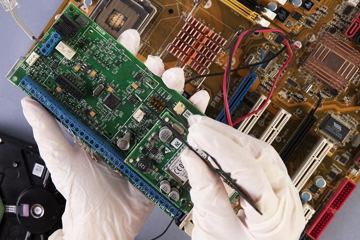
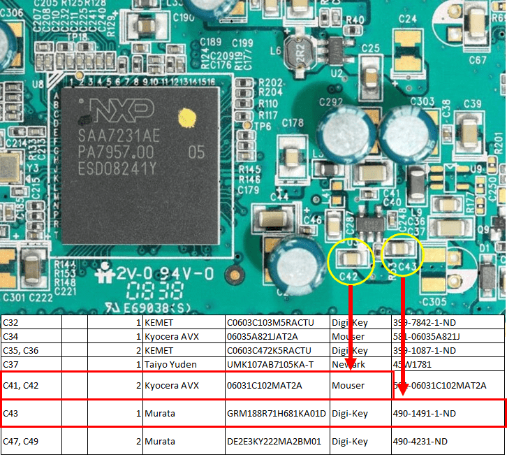
The next task is to identify each component and build a clean, structured bill of materials. This is critical if the board needs to be re‑manufactured or redesigned.
A practical approach:
- Use magnification to read every reference designator and component marking (IC codes, resistor values, capacitor labels, relay models, etc.).
- Desolder parts carefully when markings are hidden, and measure value or characteristics with multimeters and LCR meters where needed.
- For semiconductors and ICs, search manufacturers’ datasheets to identify exact part numbers and equivalents.
For obsolete parts, a simple one‑to‑one replacement is often not possible. You may need to:
- Identify modern equivalents with compatible electrical ratings, package and temperature range.
- Consider small schematic or layout changes to support new parts, especially for power devices and communication interfaces.
At the end of this step, you want a BOM with:
- Reference designator, quantity, value or rating, footprint, manufacturer and manufacturer part number where possible.
- Notes on any parts you expect to substitute, with candidate alternatives.
Step 4 – Layer and Trace Analysis
To reconstruct the schematic and layout accurately, you must understand how layers and traces are arranged. For simple two‑layer boards this can be done visually, but multilayer industrial boards often require more advanced methods.
Typical techniques:
- Use bright light and magnification to follow traces and vias on outer layers.
- For multilayer boards, use X‑ray imaging to visualize inner planes and dense BGA or driver areas.
- In difficult cases, destructive delayering (carefully sanding or milling away layers) combined with scanning of each layer can be used to reconstruct complex stackups.
During this step, you pay particular attention to:
- Power distribution and ground planes feeding motors, actuators, PLC modules or sensors.
- Differential pairs and controlled impedance traces for fieldbus or communication (CAN, RS‑485, Ethernet, etc.).
- Shielding and isolation patterns around high‑voltage or safety‑related circuits.

Step 5 – Schematic Reconstruction
With enough connectivity information, you can start rebuilding the schematic in a CAD tool. The goal is not just to “draw wires” but to recover the functional architecture of the board.
A practical way to organize the schematic:
- Split the design into logical blocks: power supplies, motor/valve drivers, PLC interface, communication, protection circuits, sensors and feedback.
- Start from known structures (e.g., buck converters, H‑bridges, relay drivers, optocoupler inputs) and fill in the connections around them.
- Use net names and notes to document assumptions, unknown parts and behavior you observe during testing.
For mechanical systems, understanding the interface between the PCB and the machinery is crucial. This includes:
- Encoder inputs, limit switches, proximity sensors and other signals that define motion and safety states.
- Relay or contactor drivers that control motors, pumps, solenoids and brakes.
Even if you cannot recover every detail, a well‑structured schematic that matches the board’s behavior will be enough for repair, reproduction or controlled redesign in many industrial projects.

Step 6 – PCB Layout Rebuild
Once you understand the board’s electrical structure, you rebuild the PCB layout in CAD. For mechanical applications, exact mechanical compatibility is usually non‑negotiable.
Key tasks:
- Create the correct board outline, mounting holes, cutouts and keep‑outs based on your measurements and photos.
- Place connectors, heat sinks, relays and other mechanically constrained parts in the same positions and orientations as the original.
- Route traces to match the original topology, especially in high‑current, high‑voltage and sensitive control areas.
For harsh mechanical environments, small layout improvements can make a big difference, such as:
- Widening high‑current traces and adding copper pours to reduce heating.
- Ensuring generous clearance around high‑voltage nodes and reinforcing solder joints for heavy components.
- Positioning components to improve airflow and ease of inspection or replacement.
Running design rule checks (DRC) and, where appropriate, basic simulations or field checks helps validate that the reconstructed layout is manufacturable and robust.
Step 7 – Design Improvements and Obsolescence Solutions
One advantage of PCB reverse engineering is that you can improve weak points while keeping the board compatible with the existing mechanical system. This is particularly important when fighting long‑term obsolescence.
Typical improvements include:
- Replacing obsolete parts with modern equivalents that offer better availability, reliability or performance.
- Strengthening input protection, surge suppression and filtering to handle noisy industrial environments.
- Updating connectors and terminal blocks to more robust or standardized versions while maintaining pinout.
- Separating safety‑critical circuits more clearly and adding diagnostic or status indicators where helpful.
When redesigning around replacement parts, you should double‑check:
- Thermal behavior under full load.
- Compatibility with the rest of the system (e.g., signal levels, timings, communication protocols).
- Any required re‑qualification or compliance testing if the equipment is certified.
Step 8 – Prototype Manufacturing and Assembly
With a completed design, the next practical step is to build prototypes. For industrial boards, it is better to start with a small batch and evaluate performance before committing to volume.
Key points for prototyping:
- Use accurate Gerber or ODB++ data, stack‑up details and fabrication notes that reflect the original board’s materials and finishes where possible.
- Match key parameters such as board thickness, copper weight and surface finish (e.g., ENIG) if these affect mechanical fit or reliability.
- Assemble the prototypes following a controlled soldering profile and quality checks, especially for fine‑pitch or high‑current parts.
A practical first run might be 5–20 units, depending on how many boards you need for lab testing, on‑site trials and spares.

Step 9 – Functional Testing in Mechanical Systems
No PCB reverse engineering project is complete until the board is tested in the real equipment. This step verifies both electrical performance and behavior in the mechanical environment.
Useful practices:
- Start with bench testing: power up the board under controlled conditions, verify voltages, communication and basic I/O, and monitor temperatures.
- Move to system testing in the machine: run the equipment through typical and edge‑case cycles, including start‑up, shut‑down and emergency stop sequences.
- Check long‑term behavior: vibration, heating, noise immunity and stability over shifts or days of operation.
Agreeing in advance with your engineering partner on clear acceptance criteria—such as temperature limits, duty cycles and fault behavior—helps avoid surprises at this stage.
Step 10 – Documentation and Long‑Term Support
A major benefit of professional reverse engineering is the documentation you gain. Instead of a mysterious “black box” board, you now have a set of files that make future work much easier.
Typical deliverables:
- Schematic files and PDFs.
- PCB layout files, Gerbers or ODB++, stack‑up information and fabrication notes.
- BOM with part numbers and any approved alternatives.
- Test procedures and basic troubleshooting notes.
With this in hand, you can:
- Order future production runs as needed without starting from scratch.
- Plan further redesigns or upgrades when technology changes again.
- Reduce dependency on any single supplier because the core design data is under your control.
Key Tools and Techniques Used in Mechanical Parts PCB Reverse Engineering
Effective reverse engineering combines careful manual work with the right tools. The goal is to collect reliable data without unnecessarily damaging the original board.
Practical hardware tools:
- Microscopes and imaging systems for reading fine markings and documenting layers.
- Desoldering and rework stations for safely removing and testing components.
- Multimeters, LCR meters, oscilloscopes and signal analyzers for probing circuits and observing behavior.
- X‑ray equipment for viewing inner layers, hidden pads and complex assemblies.
Software tools:
- PCB CAD tools for schematic capture and layout reconstruction.
- Image processing software to align and trace board photos or scans into CAD footprints and routing.
- Circuit simulation and analysis tools to verify critical sections before building prototypes.
The right combination depends on board complexity, budget and how critical the equipment is, but even modest setups can produce good results when used carefully and systematically.
How to Choose a Mechanical Parts PCB Reverse Engineering Partner in China
If you decide to work with a China‑based partner, you want more than just a “copy shop.” For mechanical and industrial boards, experience, communication and process discipline matter as much as raw technical skills.
Key evaluation points:
- Proven experience with industrial automation, robotics, construction equipment or similar mechanical sectors.
- Ability to handle the full chain: PCB reverse engineering, PCB redesign (if needed), prototyping and volume PCBA.
- Capability Across Board Complexity: confirm that the supplier routinely handles multi-layer boards (for example, 4–20 layers), BGA/QFN packages, power management circuits, and high-speed or communication interfaces commonly found in industrial control systems.
- Clear IP protection practices and willingness to sign NDAs.
- Documented testing capabilities and quality systems for industrial‑grade products.
A simple supplier screening checklist can be very helpful:
| Question to Ask | Why It Matters |
|---|---|
| Do you provide full deliverables (schematic, PCB layout, BOM, manufacturing files)? | Ensures you gain long-term control over the design |
| What layer counts and board complexities do you typically support? | Verifies capability for industrial-grade PCBs |
| How do you identify components and suggest alternatives for obsolete parts? | Critical for long-life mechanical systems |
| What functional testing or engineering verification is performed before delivery? | Indicates real-world reliability |
| How many working samples do you need, and what condition must they be in? | Clarifies project feasibility |
| Are you willing to sign an NDA and explain your data protection process? | Protects IP and sensitive information |
| How is reverse engineering pricing structured? | Helps estimate budget and scope |
FAQs about Mechanical Parts PCB Reverse Engineering
Q1. Is it legal to reverse engineer a PCB from my own industrial machine?
In many cases, analyzing and documenting a PCB inside equipment you own for purposes such as repair, maintenance or replacement is allowed, but intellectual property laws vary by country. You should avoid using reverse‑engineered designs in ways that infringe patents, copyrights or trade secrets, and when in doubt, it is sensible to consult a legal professional in your jurisdiction.
Q2. Can you reverse engineer a PCB if some components are obsolete?
Yes, obsolescence is a common driver for reverse engineering industrial PCBs, especially in long‑life equipment. The process includes identifying obsolete parts and finding modern equivalents or redesigning sections of the circuit to work with currently available components while preserving the board’s overall behavior.
Q3. What files and data will I receive after PCB reverse engineering is completed?
Typical deliverables include schematic files, PCB layout data (such as Gerbers or ODB++), a structured BOM with part numbers and any recommended alternatives, plus basic test procedures. With these, you can reproduce the board with your chosen manufacturer and maintain better control over the lifecycle of your equipment.
Q4. How long does mechanical parts PCB reverse engineering usually take?
Timeframes vary based on board complexity, the availability of samples and how much redesign is needed. Simple two‑layer boards for smaller machines can sometimes be turned around in weeks, while complex multilayer or safety‑critical boards may take several weeks to a few months, especially when multiple prototype and test cycles are required.
Q5. What is the minimum quantity for re‑manufacturing a reverse PCB?
There is no universal minimum, but for industrial applications it is common to produce an initial small batch for validation and spares, then follow with larger orders as needed. Many manufacturers will accept low volumes for critical maintenance projects, particularly when they also see potential for long‑term repeat orders.
Q6. Do I always need firmware to reverse engineer a PCB?
Not always. If the PCB’s core behavior is defined by hardware circuits and standard components, it may be possible to reverse engineer and reproduce the board without firmware access. When proprietary microcontrollers or programmable devices hold essential logic, you may need to replace or reimplement that functionality rather than copy it directly.
7. Can mechanical parts PCB reverse engineering improve safety or performance?
Yes, many projects include targeted improvements such as stronger surge protection, better isolation, more robust connectors or updated components with improved ratings. These changes can enhance reliability and safety while preserving compatibility with the existing mechanical system and control logic.

